Engineering 4862 Microprocessors Lecture 23 Cheng Li EN4012













- Slides: 42

Engineering 4862 Microprocessors Lecture 23 Cheng Li EN-4012 licheng@engr. mun. ca Engr 4862 Microprocessors

I/O Design • When designing an I/O port, ensure that the port is only active when selected by the microprocessor – Use latches (output) and buffers (input) to isolate the I/O port circuitry from the address and data bus – Use the correct combinatorial logic circuitry and/or decoders with address bus to select the port Engr 4862 Microprocessors

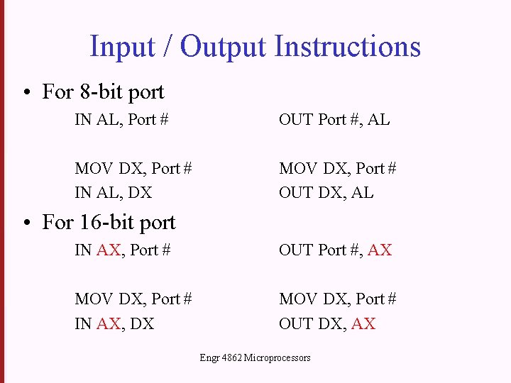
Input / Output Instructions • For 8 -bit port IN AL, Port # OUT Port #, AL MOV DX, Port # IN AL, DX MOV DX, Port # OUT DX, AL • For 16 -bit port IN AX, Port # OUT Port #, AX MOV DX, Port # IN AX, DX MOV DX, Port # OUT DX, AX Engr 4862 Microprocessors

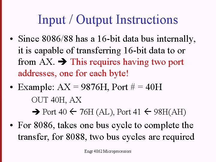
Input / Output Instructions • Since 8086/88 has a 16 -bit data bus internally, it is capable of transferring 16 -bit data to or from AX. This requires having two port addresses, one for each byte! • Example: AX = 9876 H, Port # = 40 H OUT 40 H, AX Port 40 76 H (AL), Port 41 98 H(AH) • For 8086, takes one bus cycle to complete the transfer, for 8088, two bus cycles are required Engr 4862 Microprocessors

Output Design Example: 8 LEDs • This is a byte-wide output port • The LEDs cannot be connected directly to data bus – Difficult to select the LEDs – LEDs would only display value for very short period of time (about 400 ns, or 2 clock cycles) • Only when data bus carries the correct signal – Microprocessor cannot sink enough current Engr 4862 Microprocessors

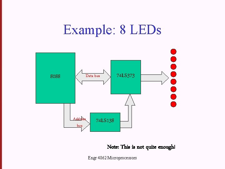
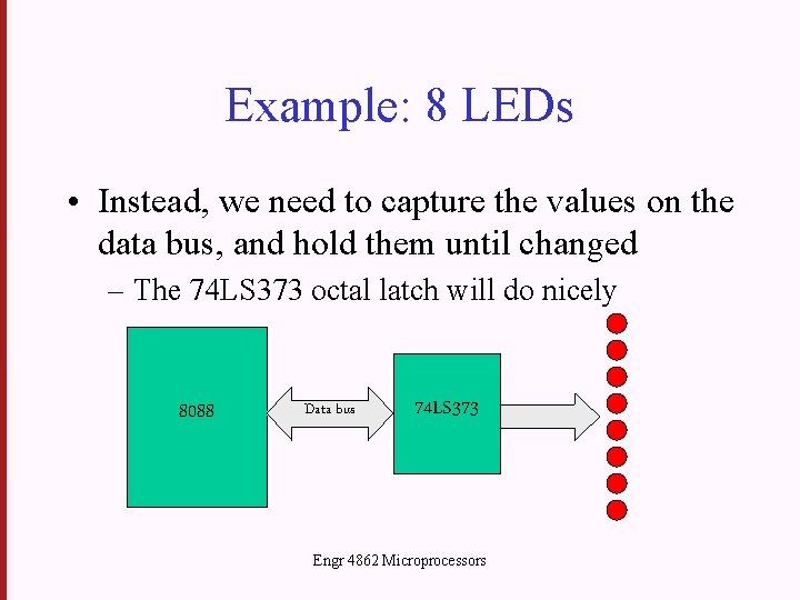
Example: 8 LEDs • Instead, we need to capture the values on the data bus, and hold them until changed – The 74 LS 373 octal latch will do nicely 8088 Data bus 74 LS 373 Engr 4862 Microprocessors

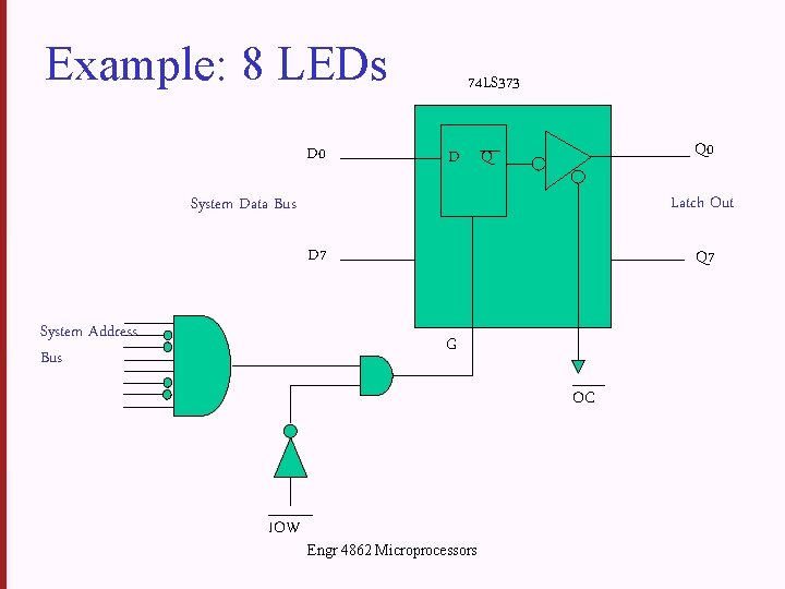
Example: 8 LEDs • We only want the latch to load values from the data bus when the microprocessor outputs to the correct port # – Suggestion 1: Decode the address directly – Suggestion 2: Use a decoder such as the 3 x 8 74 LS 138 with lines from the address bus Engr 4862 Microprocessors

Example: 8 LEDs D 0 74 LS 373 Q 0 D Q Latch Out System Data Bus D 7 System Address Bus Q 7 G OC IOW Engr 4862 Microprocessors

Example: 8 LEDs 8088 74 LS 373 Data bus Address bus 74 LS 138 Note: This is not quite enough! Engr 4862 Microprocessors

Engr 4862 Microprocessors

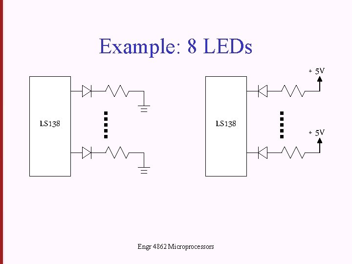
Example: 8 LEDs • How do we connect the LEDs? – 2 possibilities Engr 4862 Microprocessors

Example: 8 LEDs + 5 V LS 138 Engr 4862 Microprocessors + 5 V

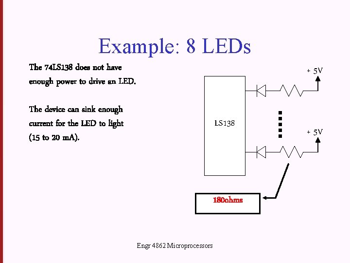
Example: 8 LEDs The 74 LS 138 does not have enough power to drive an LED. + 5 V The device can sink enough current for the LED to light (15 to 20 m. A). LS 138 180 ohms Engr 4862 Microprocessors + 5 V

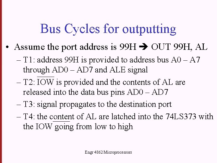
Bus Cycles for outputting • Assume the port address is 99 H OUT 99 H, AL – T 1: address 99 H is provided to address bus A 0 – A 7 through AD 0 – AD 7 and ALE signal – T 2: IOW is provided and the contents of AL are released into the data bus pins AD 0 – AD 7 – T 3: signal propagates to the destination port – T 4: the content of AL are latched into the 74 LS 373 with the IOW going from low to high Engr 4862 Microprocessors

Example: 8 LEDs • Instead, we need to capture the values on the data bus, and hold them until changed – The 74 LS 373 octal latch will do nicely 8088 Data bus 74 LS 373 Engr 4862 Microprocessors

Example: 8 LEDs • We only want the latch to load values from the data bus when the microprocessor outputs to the correct port # – Suggestion 1: Decode the address directly – Suggestion 2: Use a decoder such as the 3 x 8 74 LS 138 with lines from the address bus Engr 4862 Microprocessors

Example: 8 LEDs D 0 74 LS 373 Q 0 D Q Latch Out System Data Bus D 7 System Address Bus Q 7 G OC IOW Engr 4862 Microprocessors

Example: 8 LEDs 8088 74 LS 373 Data bus Address bus 74 LS 138 Note: This is not quite enough! Engr 4862 Microprocessors

Engr 4862 Microprocessors

Example: 8 LEDs • How do we connect the LEDs? – 2 possibilities Engr 4862 Microprocessors

Example: 8 LEDs + 5 V LS 138 Engr 4862 Microprocessors + 5 V

Example: 8 LEDs The 74 LS 138 does not have enough power to drive an LED. + 5 V The device can sink enough current for the LED to light (15 to 20 m. A). LS 138 180 ohms Engr 4862 Microprocessors + 5 V

Bus Cycles for outputting • Assume the port address is 99 H OUT 99 H, AL – T 1: address 99 H is provided to address bus A 0 – A 7 through AD 0 – AD 7 and ALE signal – T 2: IOW is provided and the contents of AL are released into the data bus pins AD 0 – AD 7 – T 3: signal propagates to the destination port – T 4: the content of AL are latched into the 74 LS 373 with the IOW going from low to high Engr 4862 Microprocessors

Engr 4862 Microprocessors

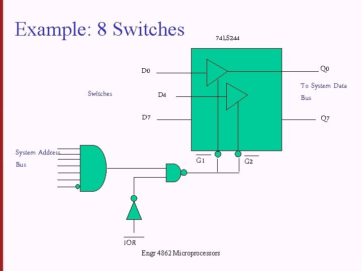
Example: 8 Switches • Now we will look at an 8 -bit input port. • The procedure to select the port is similar to the output case – Use IORD* instead of IOWR* Engr 4862 Microprocessors

Example: 8 Switches • We cannot use a latch to separate the switches from the microprocessor – We only want the switch values to be on the data bus when the microprocessor asks for it – A latch would constantly drive the bus! Engr 4862 Microprocessors

Example: 8 Switches • The device of interest here is the 74 LS 244 tristate buffer (unidirectional) – NOT the same as the 74 LS 245 transceiver (bidirectional) • Tristate: – One of three states: on (1), off (0), or open (Z) – In the open state, the buffer does not drive the data bus Engr 4862 Microprocessors

Engr 4862 Microprocessors

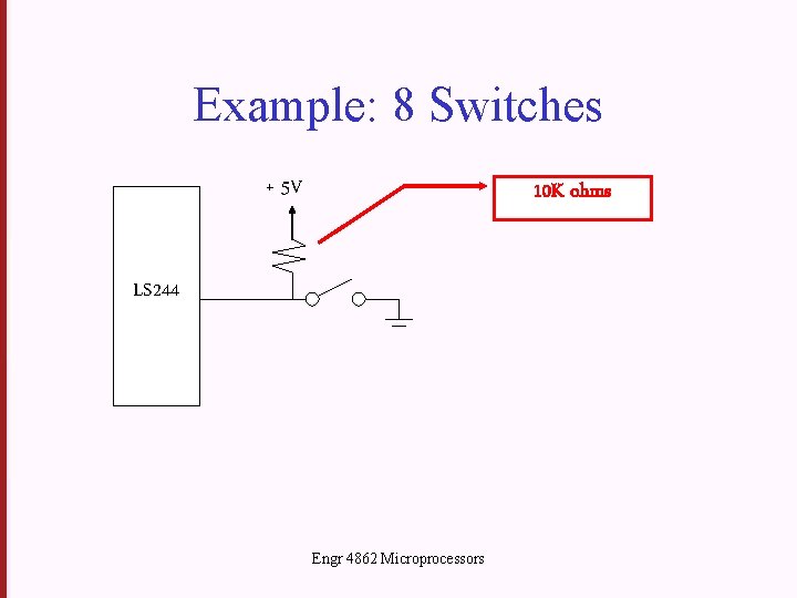
Example: 8 Switches • How do we set up the switches? – When open, one logic level – When closed, the other logic level Engr 4862 Microprocessors

Example: 8 Switches + 5 V 10 K ohms LS 244 Engr 4862 Microprocessors

Example: 8 Switches 74 LS 244 Q 0 D 0 Switches To System Data Bus D 4 D 7 System Address Bus Q 7 G 1 IOR Engr 4862 Microprocessors G 2

Summary • Since the data provided by the CPU to the port is on the system data bus for a limited amount of time (501000 ns), it must be latched before it is lost • In order to prevent any unwanted data from coming into the system data bus, all input devices must isolated through the tri-state buffer – The 74 LS 244 not only plays this role, but also provides the incoming signals sufficient strength (boosting) to travel all the ways to the CPU. • As general, every device (memory, peripherals) connected to the global data bus must have a latch ot tristate buffer Engr 4862 Microprocessors

Engr 4862 Microprocessors

Programmable I/O • The previous examples are good for many applications, but sometimes a more powerful and flexible solution is needed. • The 8255 Programmable Peripheral Interface (PPI) is a 40 -pin DIP IC that provides 3 programmable I/O ports, A, B, and C. • One can program the individual port to be input or output port, economical and flexible than 74 LS 373, 73 LS 244, which must be hard wired) Engr 4862 Microprocessors

Programmable I/O • How are is it programmable? – Configure each port as input or output – Different modes of operation • You must initialize the PPI via software commands – Send a control byte to the device’s control register port Engr 4862 Microprocessors

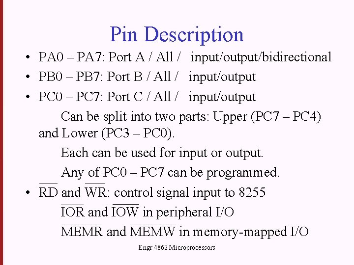
Pin Description • PA 0 – PA 7: Port A / All / input/output/bidirectional • PB 0 – PB 7: Port B / All / input/output • PC 0 – PC 7: Port C / All / input/output Can be split into two parts: Upper (PC 7 – PC 4) and Lower (PC 3 – PC 0). Each can be used for input or output. Any of PC 0 – PC 7 can be programmed. • RD and WR: control signal input to 8255 IOR and IOW in peripheral I/O MEMR and MEMW in memory-mapped I/O Engr 4862 Microprocessors

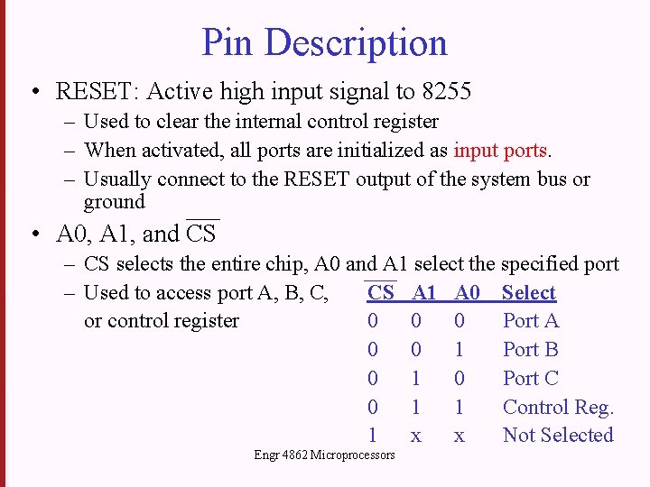
Pin Description • RESET: Active high input signal to 8255 – Used to clear the internal control register – When activated, all ports are initialized as input ports. – Usually connect to the RESET output of the system bus or ground • A 0, A 1, and CS – CS selects the entire chip, A 0 and A 1 select the specified port – Used to access port A, B, C, CS A 1 A 0 Select or control register 0 0 0 Port A 0 0 1 Port B 0 1 0 Port C 0 1 1 Control Reg. 1 x x Not Selected Engr 4862 Microprocessors

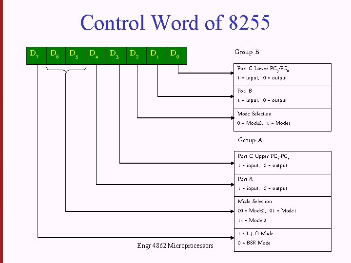
Control Word of 8255 D 7 D 6 D 5 D 4 D 3 D 2 D 1 D 0 Group B Port C Lower PC 3 -PC 0 1 = input, 0 = output Port B 1 = input, 0 = output Mode Selection 0 = Mode 0, 1 = Mode 1 Group A Port C Upper PC 7 -PC 4 1 = input, 0 = output Port A 1 = input, 0 = output Mode Selection 00 = Mode 0, 01 = Mode 1 1 x = Mode 2 Engr 4862 Microprocessors 1 = I / O Mode 0 = BSR Mode

Mode Selection • It’s the control register that must be programmed to select the operation mode of the three ports: A, B, and C • The 8255 chip is programmed in any of the above modes by sending a byte (control word) to the control register of the 8255 Engr 4862 Microprocessors

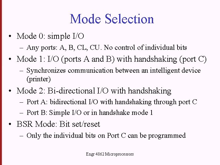
Mode Selection • Mode 0: simple I/O – Any ports: A, B, CL, CU. No control of individual bits • Mode 1: I/O (ports A and B) with handshaking (port C) – Synchronizes communication between an intelligent device (printer) • Mode 2: Bi-directional I/O with handshaking – Port A: bidirectional I/O with handshaking through port C – Port B: Simple I/O or in handshake mode 1 • BSR Mode: Bit set/reset – Only the individual bits on Port C can be programmed Engr 4862 Microprocessors

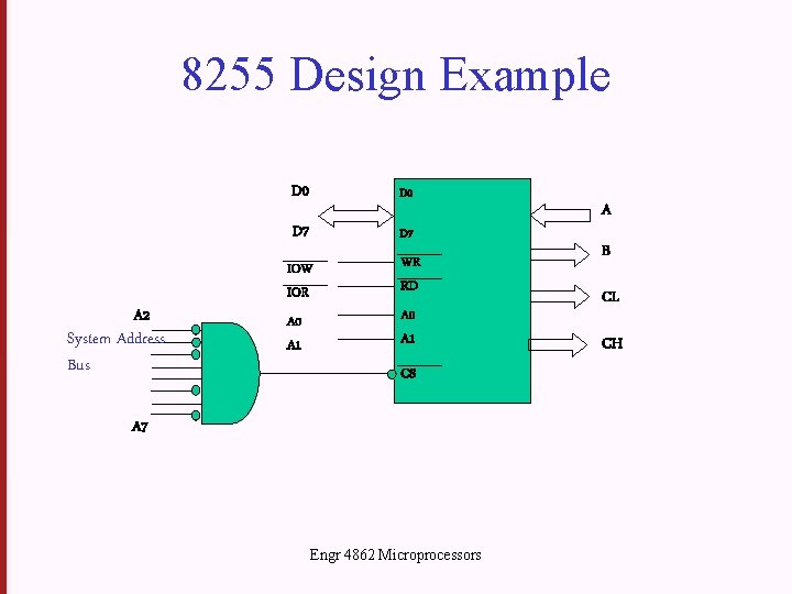
8255 Design Example • Mode 0 – Any of ports A, B, C can be programmed as input or output – Port can not be both an input and output port at the same time – Port C can be programmed with CL, CH separately – Example: Engr 4862 Microprocessors

8255 Design Example A 2 System Address Bus D 0 D 7 IOW IOR WR RD A 0 A 1 CS A 7 Engr 4862 Microprocessors A B CL CH