Engineering 4862 Microprocessors Lecture 22 Cheng Li EN4012


- Slides: 54

Engineering 4862 Microprocessors Lecture 22 Cheng Li EN-4012 licheng@engr. mun. ca Engr 4862 Microprocessors

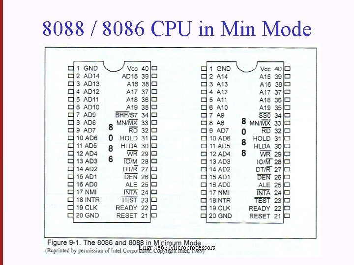
8088 / 8086 CPU in Mode Engr 4862 Microprocessors

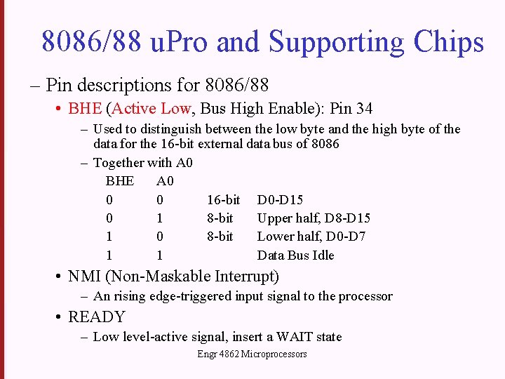
8086/88 u. Pro and Supporting Chips – Pin descriptions for 8086/88 • BHE (Active Low, Bus High Enable): Pin 34 – Used to distinguish between the low byte and the high byte of the data for the 16 -bit external data bus of 8086 – Together with A 0 BHE A 0 0 0 16 -bit D 0 -D 15 0 1 8 -bit Upper half, D 8 -D 15 1 0 8 -bit Lower half, D 0 -D 7 1 1 Data Bus Idle • NMI (Non-Maskable Interrupt) – An rising edge-triggered input signal to the processor • READY – Low level-active signal, insert a WAIT state Engr 4862 Microprocessors

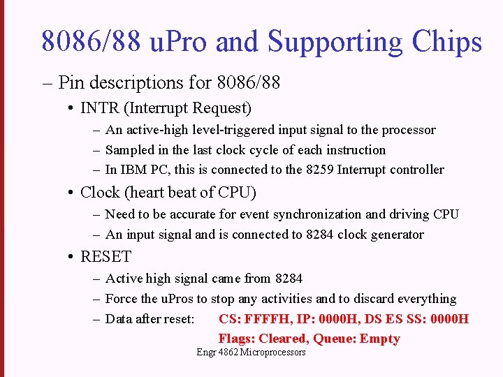
8086/88 u. Pro and Supporting Chips – Pin descriptions for 8086/88 • INTR (Interrupt Request) – An active-high level-triggered input signal to the processor – Sampled in the last clock cycle of each instruction – In IBM PC, this is connected to the 8259 Interrupt controller • Clock (heart beat of CPU) – Need to be accurate for event synchronization and driving CPU – An input signal and is connected to 8284 clock generator • RESET – Active high signal came from 8284 – Force the u. Pros to stop any activities and to discard everything – Data after reset: CS: FFFFH, IP: 0000 H, DS ES SS: 0000 H Flags: Cleared, Queue: Empty Engr 4862 Microprocessors

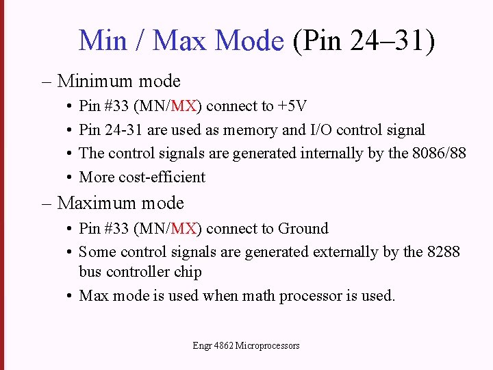
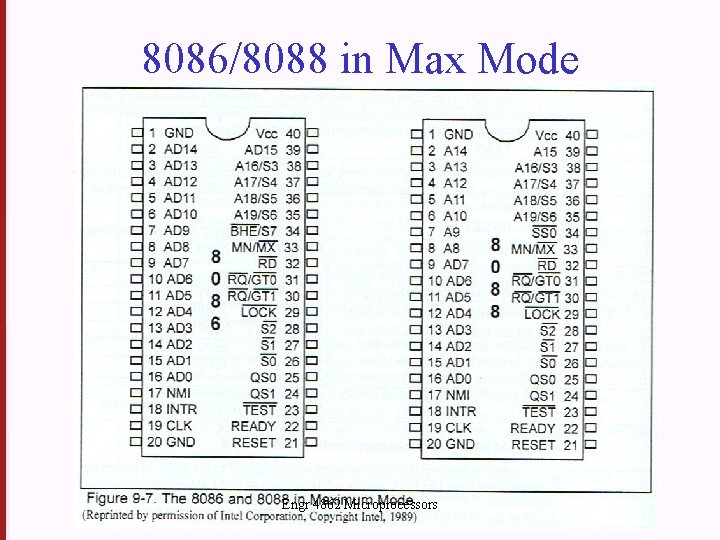
Min / Max Mode (Pin 24– 31) – Minimum mode • • Pin #33 (MN/MX) connect to +5 V Pin 24 -31 are used as memory and I/O control signal The control signals are generated internally by the 8086/88 More cost-efficient – Maximum mode • Pin #33 (MN/MX) connect to Ground • Some control signals are generated externally by the 8288 bus controller chip • Max mode is used when math processor is used. Engr 4862 Microprocessors

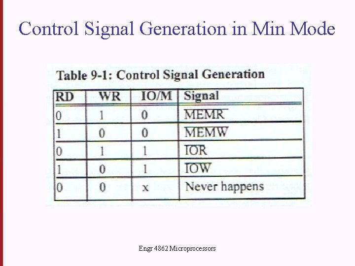
Control Signal Generation in Mode Engr 4862 Microprocessors

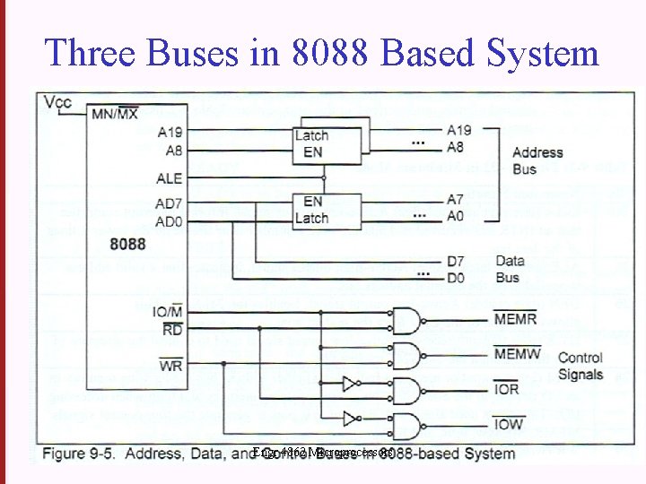
Three Buses in 8088 Based System Engr 4862 Microprocessors

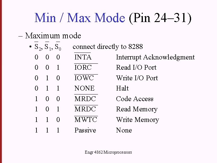
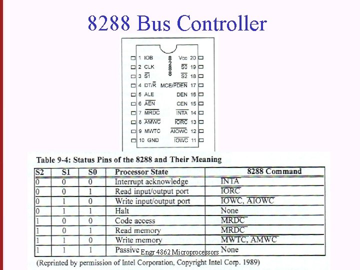
Min / Max Mode (Pin 24– 31) – Maximum mode • S 2, S 1, S 0 0 0 1 1 1 0 0 1 1 1 connect directly to 8288 INTA Interrupt Acknowledgment IORC Read I/O Port IOWC Write I/O Port NONE Halt MRDC Code Access MRDC Read Memory MWTC Write Memory Passive None Engr 4862 Microprocessors

8086/8088 in Max Mode Engr 4862 Microprocessors

8288 Bus Controller Engr 4862 Microprocessors

The Clock • The clock signal is very important to the operation of a microprocessor circuit. • It synchronizes the sequential activities of the CPU and the system – Not all devices use a clock signal (eg. PPI) Engr 4862 Microprocessors

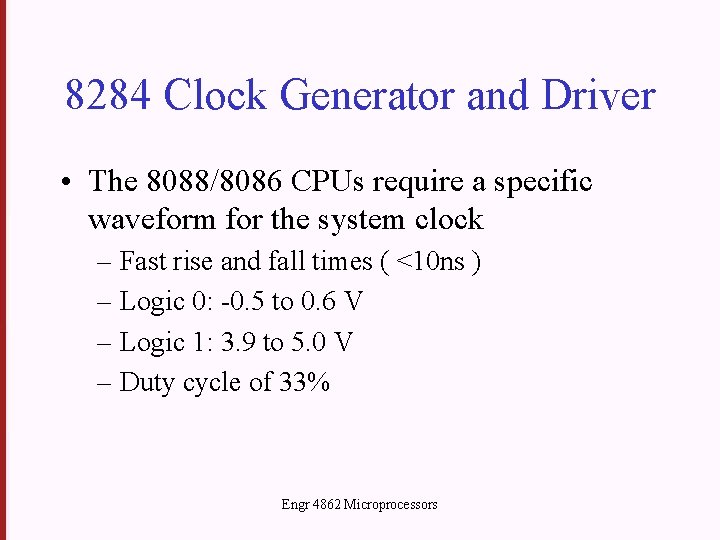
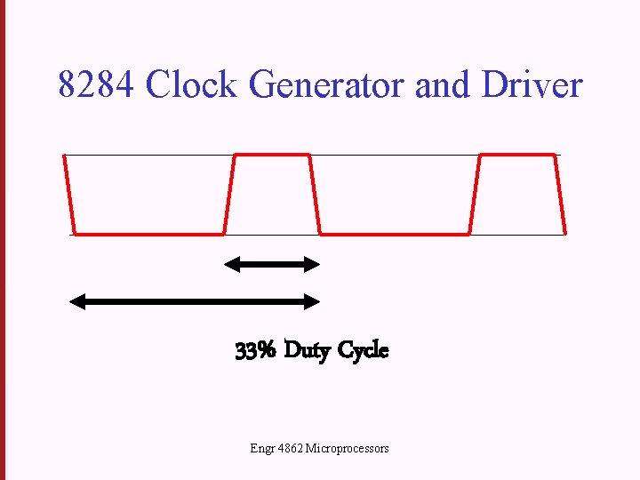
8284 Clock Generator and Driver • The 8088/8086 CPUs require a specific waveform for the system clock – Fast rise and fall times ( <10 ns ) – Logic 0: -0. 5 to 0. 6 V – Logic 1: 3. 9 to 5. 0 V – Duty cycle of 33% Engr 4862 Microprocessors

8284 Clock Generator and Driver 33% Duty Cycle Engr 4862 Microprocessors

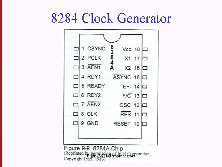
8284 Clock Generator Engr 4862 Microprocessors

8284 Clock Generator and Driver • The 8284 provides the proper clock signal – Uses a crystal oscillator (3 oscillations per clock) • Provides the correct waveforms for other signals to CPU – RESET – Request for wait state Engr 4862 Microprocessors

8284 Clock Generator and Driver – An 18 -pin chip. Not only provide the clock and synchronization for the microprocessor, but also provides the READY signal for the insertion of WAIT states into the CPU bus cycle. – Input Pins • RES (Reset In): from power supplier • X 1 and X 2 (Crystal In): the crystal frequency must be 3 times the desired frequency for the microprocessor – For IBM PC, 14. 31818 MHz (max 24 MHz) • RDY 1 and AEN 1: provide a Ready signal to the m. Pro, which will insert a WAIT state to the CPU read/write cycle. • RDY 2 and AEN 2: For multiprocessor systems Engr 4862 Microprocessors

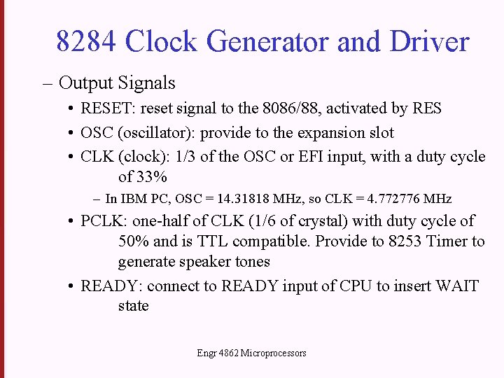
8284 Clock Generator and Driver – Output Signals • RESET: reset signal to the 8086/88, activated by RES • OSC (oscillator): provide to the expansion slot • CLK (clock): 1/3 of the OSC or EFI input, with a duty cycle of 33% – In IBM PC, OSC = 14. 31818 MHz, so CLK = 4. 772776 MHz • PCLK: one-half of CLK (1/6 of crystal) with duty cycle of 50% and is TTL compatible. Provide to 8253 Timer to generate speaker tones • READY: connect to READY input of CPU to insert WAIT state Engr 4862 Microprocessors

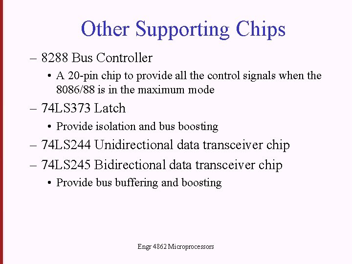
Other Supporting Chips – 8288 Bus Controller • A 20 -pin chip to provide all the control signals when the 8086/88 is in the maximum mode – 74 LS 373 Latch • Provide isolation and bus boosting – 74 LS 244 Unidirectional data transceiver chip – 74 LS 245 Bidirectional data transceiver chip • Provide bus buffering and boosting Engr 4862 Microprocessors

Machine Cycles • Also Bus Cycles • Definition: – One discrete information transfer on the buses. • This includes the address, data, and control information. Engr 4862 Microprocessors

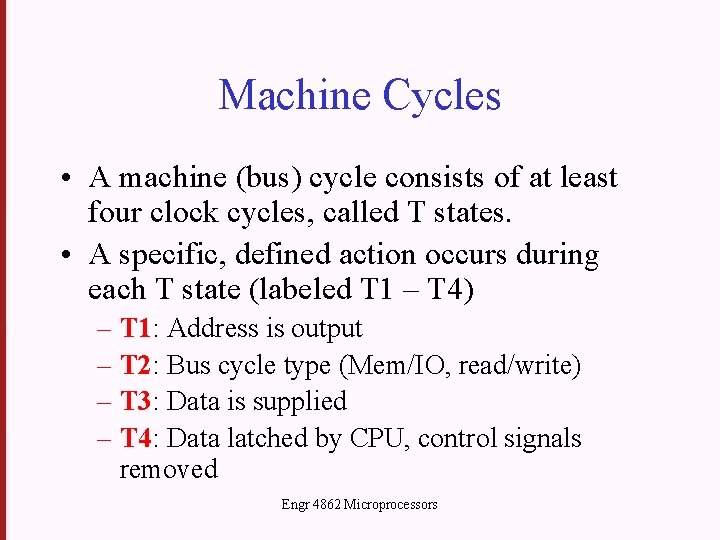
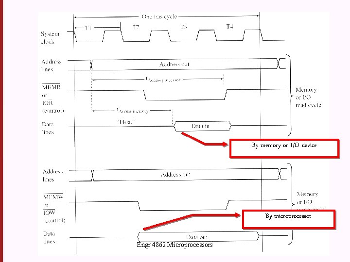
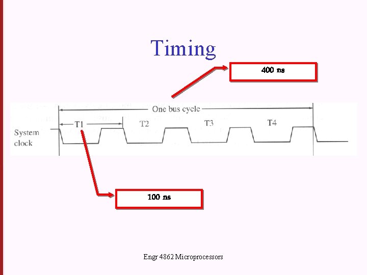
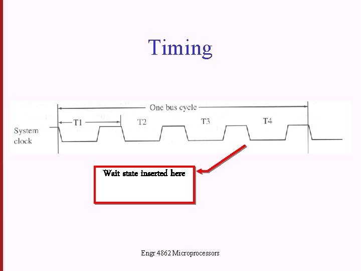
Machine Cycles • A machine (bus) cycle consists of at least four clock cycles, called T states. • A specific, defined action occurs during each T state (labeled T 1 – T 4) – T 1: Address is output – T 2: Bus cycle type (Mem/IO, read/write) – T 3: Data is supplied – T 4: Data latched by CPU, control signals removed Engr 4862 Microprocessors

By memory or I/O device By microprocessor Engr 4862 Microprocessors

T States • Why are there T states? – In the 8086/8088, the address and data lines are multiplexed. – The microprocessor needs time to change the signals during each bus cycle. – Memory devices need time to decipher the address value and then read/write the data (access time) Engr 4862 Microprocessors

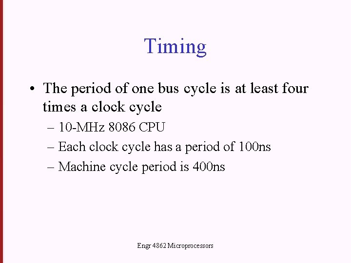
Timing • The period of one bus cycle is at least four times a clock cycle – 10 -MHz 8086 CPU – Each clock cycle has a period of 100 ns – Machine cycle period is 400 ns Engr 4862 Microprocessors

Timing 400 ns 100 ns Engr 4862 Microprocessors

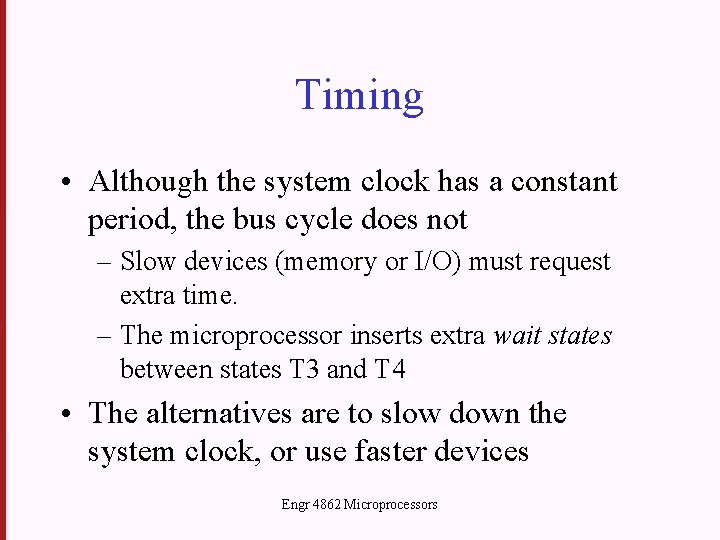
Timing • Although the system clock has a constant period, the bus cycle does not – Slow devices (memory or I/O) must request extra time. – The microprocessor inserts extra wait states between states T 3 and T 4 • The alternatives are to slow down the system clock, or use faster devices Engr 4862 Microprocessors

Timing Wait state inserted here Engr 4862 Microprocessors

I/O Design • When designing an I/O port, ensure that the port is only active when selected by the microprocessor – Use latches (output) and buffers (input) to isolate the I/O port circuitry from the address and data bus – Use the correct combinatorial logic circuitry and/or decoders with address bus to select the port Engr 4862 Microprocessors

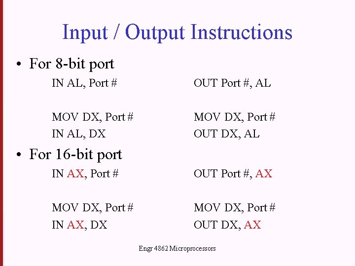
Input / Output Instructions • For 8 -bit port IN AL, Port # OUT Port #, AL MOV DX, Port # IN AL, DX MOV DX, Port # OUT DX, AL • For 16 -bit port IN AX, Port # OUT Port #, AX MOV DX, Port # IN AX, DX MOV DX, Port # OUT DX, AX Engr 4862 Microprocessors

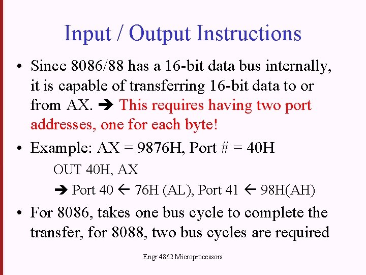
Input / Output Instructions • Since 8086/88 has a 16 -bit data bus internally, it is capable of transferring 16 -bit data to or from AX. This requires having two port addresses, one for each byte! • Example: AX = 9876 H, Port # = 40 H OUT 40 H, AX Port 40 76 H (AL), Port 41 98 H(AH) • For 8086, takes one bus cycle to complete the transfer, for 8088, two bus cycles are required Engr 4862 Microprocessors

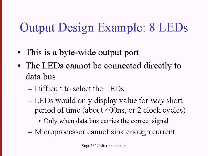
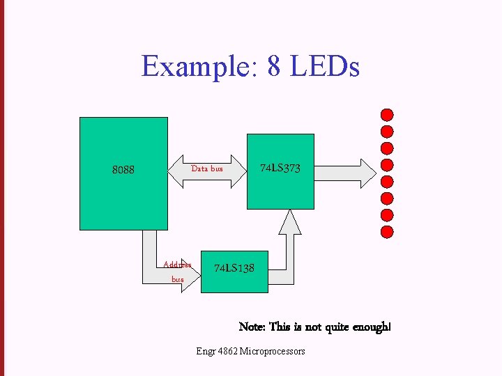
Output Design Example: 8 LEDs • This is a byte-wide output port • The LEDs cannot be connected directly to data bus – Difficult to select the LEDs – LEDs would only display value for very short period of time (about 400 ns, or 2 clock cycles) • Only when data bus carries the correct signal – Microprocessor cannot sink enough current Engr 4862 Microprocessors

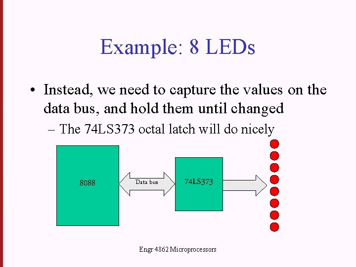
Example: 8 LEDs • Instead, we need to capture the values on the data bus, and hold them until changed – The 74 LS 373 octal latch will do nicely 8088 Data bus 74 LS 373 Engr 4862 Microprocessors

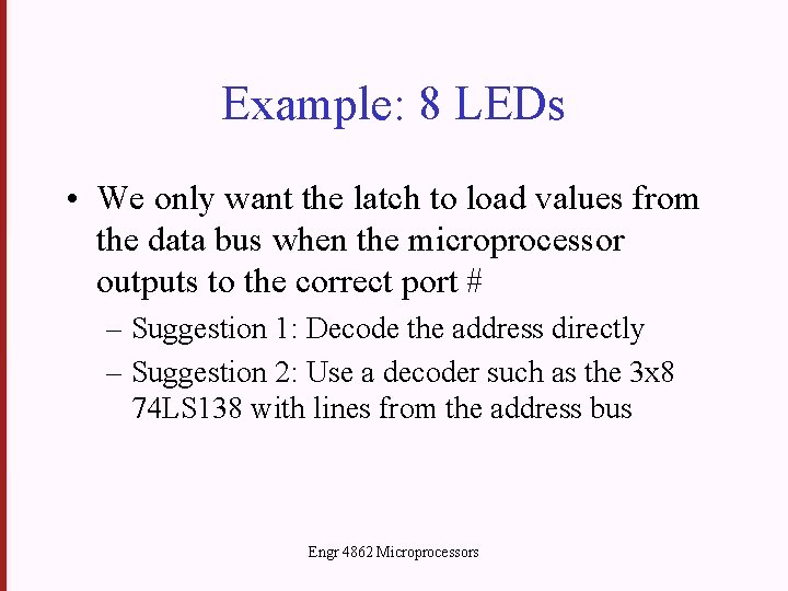
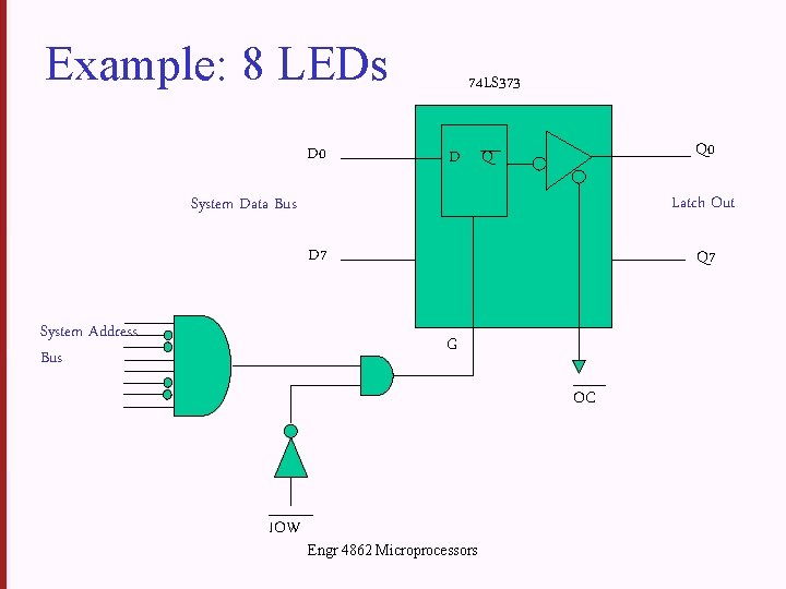
Example: 8 LEDs • We only want the latch to load values from the data bus when the microprocessor outputs to the correct port # – Suggestion 1: Decode the address directly – Suggestion 2: Use a decoder such as the 3 x 8 74 LS 138 with lines from the address bus Engr 4862 Microprocessors

Example: 8 LEDs D 0 74 LS 373 Q 0 D Q Latch Out System Data Bus D 7 System Address Bus Q 7 G OC IOW Engr 4862 Microprocessors

Example: 8 LEDs 8088 74 LS 373 Data bus Address bus 74 LS 138 Note: This is not quite enough! Engr 4862 Microprocessors

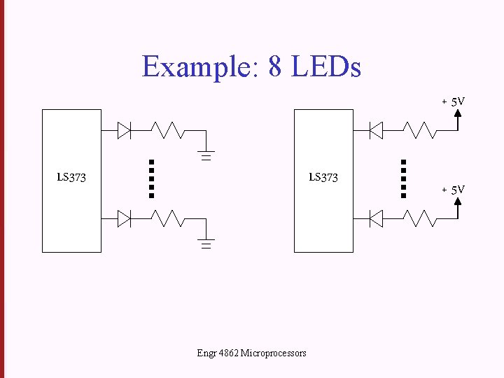
Example: 8 LEDs • How do we connect the LEDs? – 2 possibilities Engr 4862 Microprocessors

Example: 8 LEDs + 5 V LS 373 Engr 4862 Microprocessors + 5 V

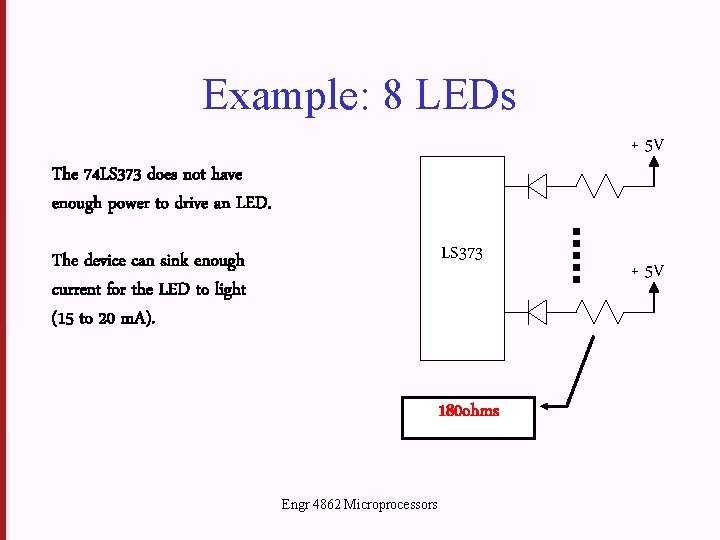
Example: 8 LEDs + 5 V The 74 LS 373 does not have enough power to drive an LED. LS 373 The device can sink enough current for the LED to light (15 to 20 m. A). 180 ohms Engr 4862 Microprocessors + 5 V

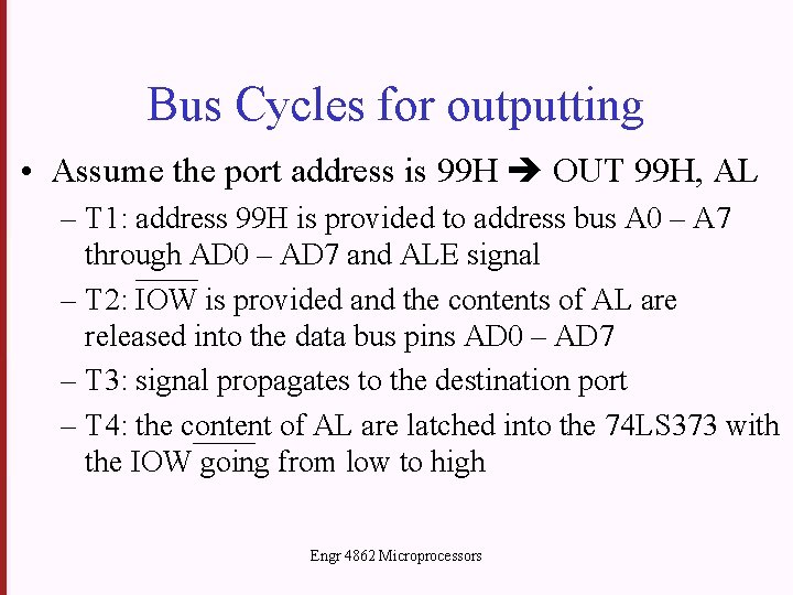
Bus Cycles for outputting • Assume the port address is 99 H OUT 99 H, AL – T 1: address 99 H is provided to address bus A 0 – A 7 through AD 0 – AD 7 and ALE signal – T 2: IOW is provided and the contents of AL are released into the data bus pins AD 0 – AD 7 – T 3: signal propagates to the destination port – T 4: the content of AL are latched into the 74 LS 373 with the IOW going from low to high Engr 4862 Microprocessors

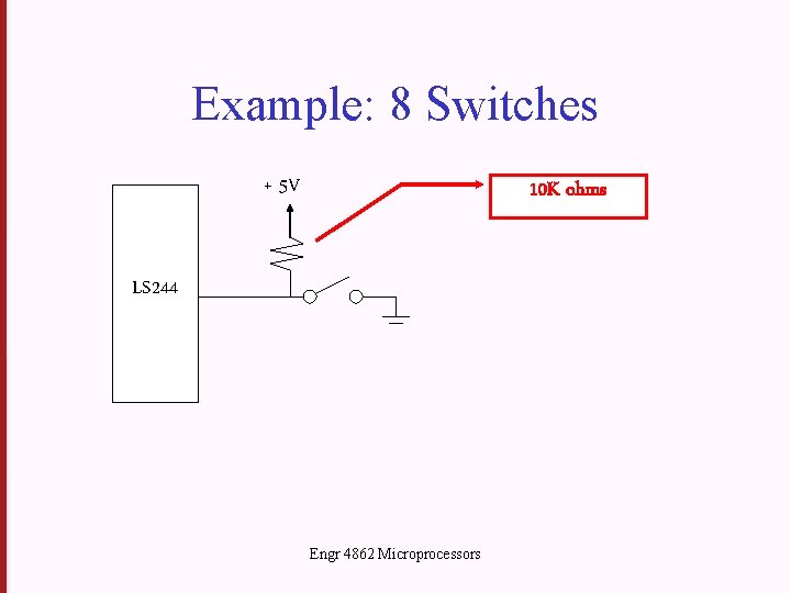
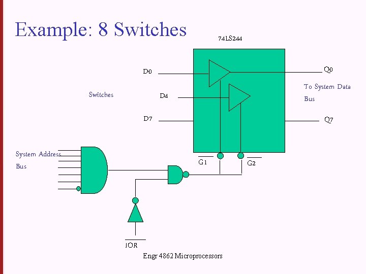
Example: 8 Switches • Now we will look at an 8 -bit input port. • The procedure to select the port is similar to the output case – Use IORD* instead of IOWR* Engr 4862 Microprocessors

Example: 8 Switches • We cannot use a latch to separate the switches from the microprocessor – We only want the switch values to be on the data bus when the microprocessor asks for it – A latch would constantly drive the bus! Engr 4862 Microprocessors

Example: 8 Switches • The device of interest here is the 74 LS 244 tristate buffer (unidirectional) – NOT the same as the 74 LS 245 transceiver (bidirectional) • Tristate: – One of three states: on (1), off (0), or open (Z) – In the open state, the buffer does not drive the data bus Engr 4862 Microprocessors

Example: 8 Switches • How do we set up the switches? – When open, one logic level – When closed, the other logic level Engr 4862 Microprocessors

Example: 8 Switches + 5 V 10 K ohms LS 244 Engr 4862 Microprocessors

Example: 8 Switches 74 LS 244 Q 0 D 0 Switches To System Data Bus D 4 D 7 System Address Bus Q 7 G 1 IOR Engr 4862 Microprocessors G 2

Summary • Since the data provided by the CPU to the port is on the system data bus for a limited amount of time (501000 ns), it must be latched before it is lost • In order to prevent any unwanted data from coming into the system data bus, all input devices must isolated through the tri-state buffer – The 74 LS 244 not only plays this role, but also provides the incoming signals sufficient strength (boosting) to travel all the ways to the CPU. • As general, every device (memory, peripherals) connected to the global data bus must have a latch ot tristate buffer Engr 4862 Microprocessors

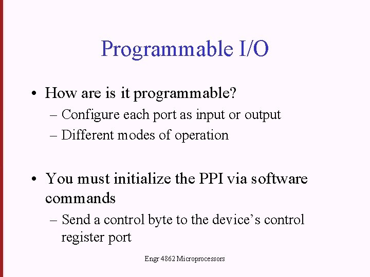
Programmable I/O • The previous examples are good for many applications, but sometimes a more powerful and flexible solution is needed. • The 8255 Programmable Peripheral Interface (PPI) is a 40 -pin DIP IC that provides 3 programmable I/O ports, A, B, and C. • One can program the individual port to be input or output port, economical and flexible than 74 LS 373, 73 LS 244, which must be hard wired) Engr 4862 Microprocessors

Programmable I/O • How are is it programmable? – Configure each port as input or output – Different modes of operation • You must initialize the PPI via software commands – Send a control byte to the device’s control register port Engr 4862 Microprocessors

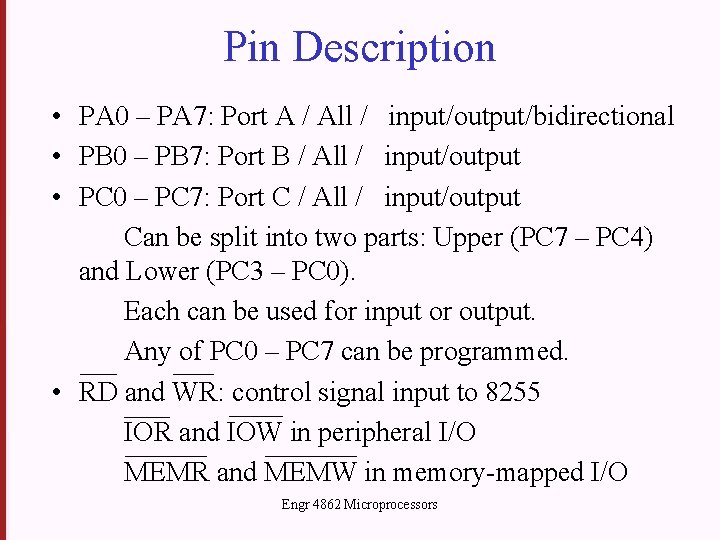
Pin Description • PA 0 – PA 7: Port A / All / input/output/bidirectional • PB 0 – PB 7: Port B / All / input/output • PC 0 – PC 7: Port C / All / input/output Can be split into two parts: Upper (PC 7 – PC 4) and Lower (PC 3 – PC 0). Each can be used for input or output. Any of PC 0 – PC 7 can be programmed. • RD and WR: control signal input to 8255 IOR and IOW in peripheral I/O MEMR and MEMW in memory-mapped I/O Engr 4862 Microprocessors

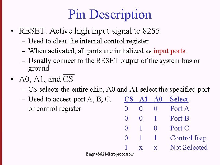
Pin Description • RESET: Active high input signal to 8255 – Used to clear the internal control register – When activated, all ports are initialized as input ports. – Usually connect to the RESET output of the system bus or ground • A 0, A 1, and CS – CS selects the entire chip, A 0 and A 1 select the specified port – Used to access port A, B, C, CS A 1 A 0 Select or control register 0 0 0 Port A 0 0 1 Port B 0 1 0 Port C 0 1 1 Control Reg. 1 x x Not Selected Engr 4862 Microprocessors

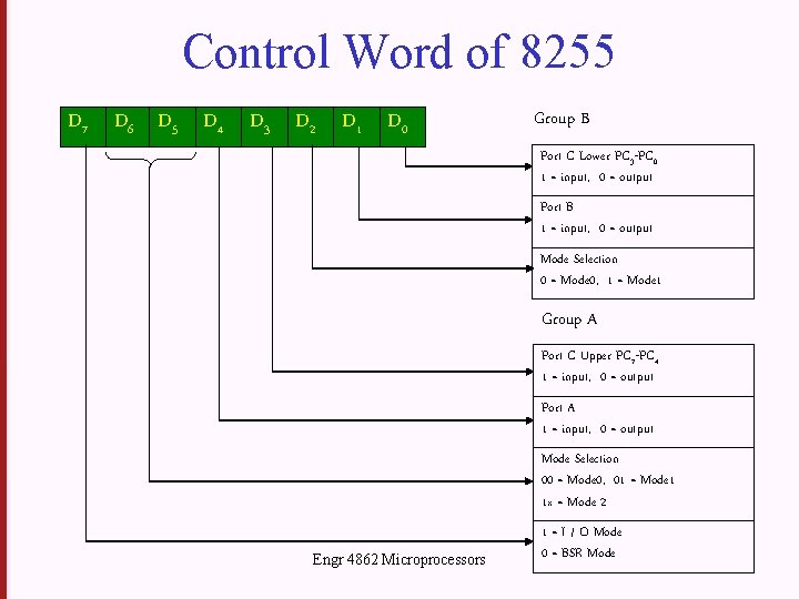
Control Word of 8255 D 7 D 6 D 5 D 4 D 3 D 2 D 1 D 0 Group B Port C Lower PC 3 -PC 0 1 = input, 0 = output Port B 1 = input, 0 = output Mode Selection 0 = Mode 0, 1 = Mode 1 Group A Port C Upper PC 7 -PC 4 1 = input, 0 = output Port A 1 = input, 0 = output Mode Selection 00 = Mode 0, 01 = Mode 1 1 x = Mode 2 Engr 4862 Microprocessors 1 = I / O Mode 0 = BSR Mode

Mode Selection • It’s the control register that must be programmed to select the operation mode of the three ports: A, B, and C • The 8255 chip is programmed in any of the above modes by sending a byte (control word) to the control register of the 8255 Engr 4862 Microprocessors

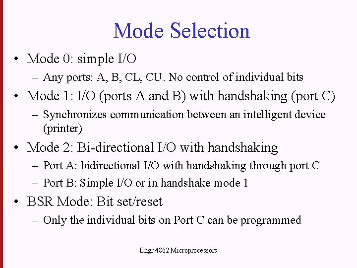
Mode Selection • Mode 0: simple I/O – Any ports: A, B, CL, CU. No control of individual bits • Mode 1: I/O (ports A and B) with handshaking (port C) – Synchronizes communication between an intelligent device (printer) • Mode 2: Bi-directional I/O with handshaking – Port A: bidirectional I/O with handshaking through port C – Port B: Simple I/O or in handshake mode 1 • BSR Mode: Bit set/reset – Only the individual bits on Port C can be programmed Engr 4862 Microprocessors

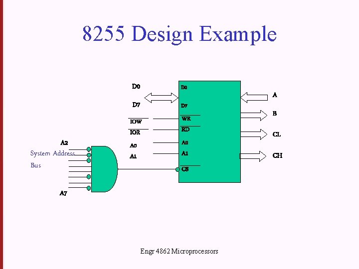
8255 Design Example A 2 System Address Bus D 0 D 7 IOW IOR WR RD A 0 A 1 CS A 7 Engr 4862 Microprocessors A B CL CH

8255 Design Example • Mode 0 – Any of ports A, B, C can be programmed as input or output – Port can not be both an input and output port at the same time – Port C can be programmed with CL, CH separately – Example: Engr 4862 Microprocessors