Engineered for Tomorrow Subject Name Fundamentals Of CMOS
Engineered for Tomorrow Subject Name: Fundamentals Of CMOS VLSI Subject Code: 10 EC 56 Prepared By: Aswini N, Praphul M N Department: ECE Date: 10/11/2014 Engineered for Tomorrow Prepared by : MN PRAPHUL & ASWINI N Assistant professor ECE Department Date : 11/10/14
Engineered for for. Tomorrow Unit 2 Circuit design process
Engineered for for. Tomorrow Syllabus q. MOS Layers. q. Stick diagram. q. Design rules and layout q. Examples
Engineered for for. Tomorrow MOS layers MOS circuits are formed on four basic layers: Ø N-diffusion Ø Polysilicon Ø Metal • These layers are isolated by one another by thick or thin silicon dioxide insulating layers. • Thin oxide mask region includes n-diffusion / p-diffusion and transistor channel.
Engineered for for. Tomorrow Stick diagrams • Stick diagrams may be used to convey layer information through the use of a color code. • For example: Ø n-diffusion --green Ø poly -- red Ø blue -- metal Ø yellow --implant Ø black --contact areas
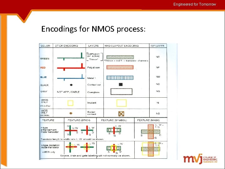
Engineered for for. Tomorrow Encodings for NMOS process:
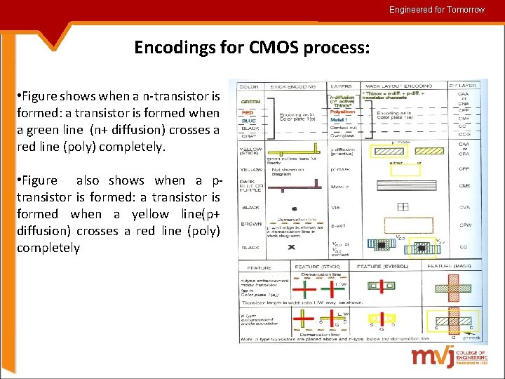
Engineered for for. Tomorrow Encodings for CMOS process: • Figure shows when a n-transistor is formed: a transistor is formed when a green line (n+ diffusion) crosses a red line (poly) completely. • Figure also shows when a ptransistor is formed: a transistor is formed when a yellow line(p+ diffusion) crosses a red line (poly) completely
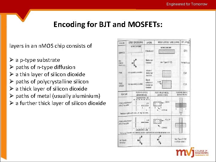
Engineered for for. Tomorrow Encoding for BJT and MOSFETs: layers in an n. MOS chip consists of Ø a p-type substrate Ø paths of n-type diffusion Ø a thin layer of silicon dioxide Ø paths of polycrystalline silicon Ø a thick layer of silicon dioxide Ø paths of metal (usually aluminium) Ø a further thick layer of silicon dioxide
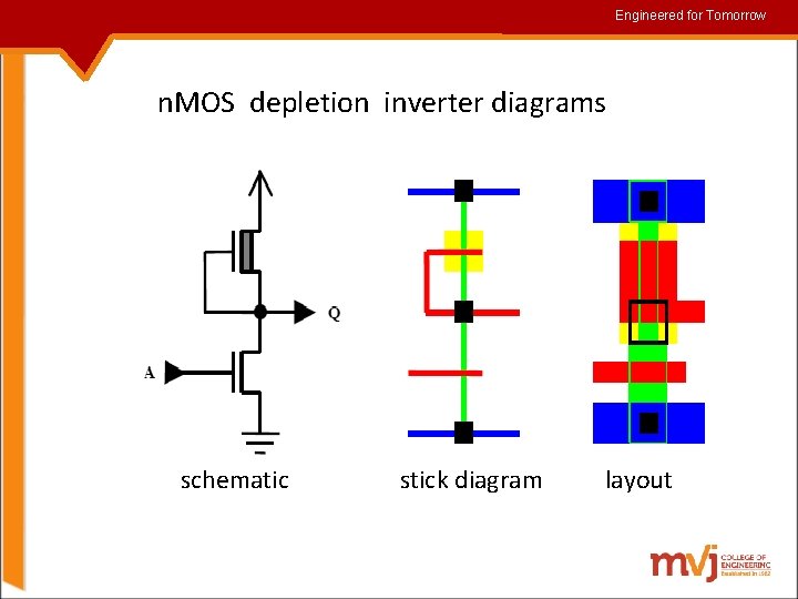
Engineered for for. Tomorrow n. MOS depletion inverter diagrams schematic stick diagram layout
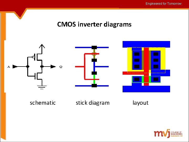
Engineered for for. Tomorrow CMOS inverter diagrams schematic stick diagram layout
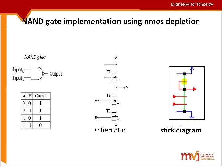
Engineered for for. Tomorrow NAND gate implementation using nmos depletion schematic stick diagram
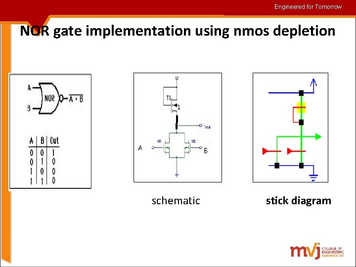
Engineered for for. Tomorrow NOR gate implementation using nmos depletion schematic stick diagram
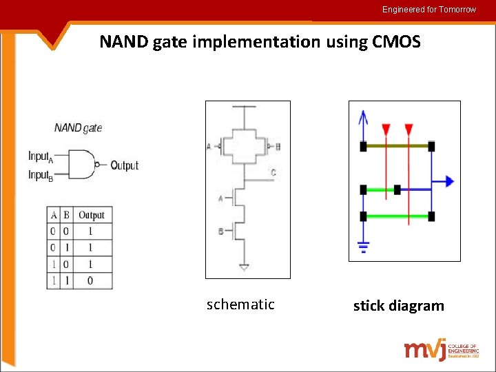
Engineered for for. Tomorrow NAND gate implementation using CMOS schematic stick diagram
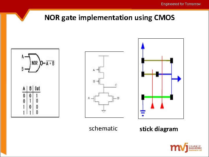
Engineered for for. Tomorrow NOR gate implementation using CMOS schematic stick diagram
Engineered for for. Tomorrow Lambda based Design Rules: ØDesign rules include width rules and spacing rules. ØMead and Conway developed a set of simplified scalable λ -based design rules, which are valid for a range of fabrication technologies. ØIn these rules, the minimum feature size of a technology is characterized as 2 λ. Ø All width and spacing rules are specified in terms of the parameter λ.
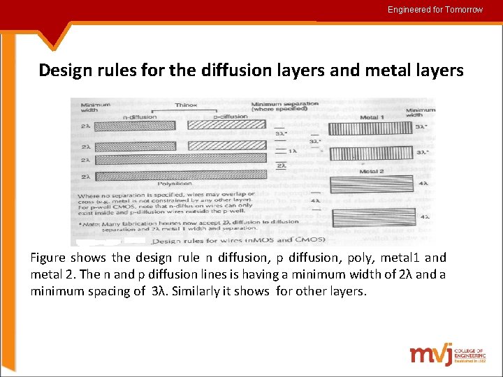
Engineered for for. Tomorrow Design rules for the diffusion layers and metal layers Figure shows the design rule n diffusion, poly, metal 1 and metal 2. The n and p diffusion lines is having a minimum width of 2λ and a minimum spacing of 3λ. Similarly it shows for other layers.
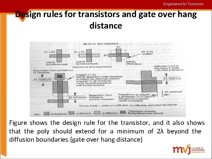
Engineered for for. Tomorrow Design rules for transistors and gate over hang distance Figure shows the design rule for the transistor, and it also shows that the poly should extend for a minimum of 2λ beyond the diffusion boundaries. (gate over hang distance)
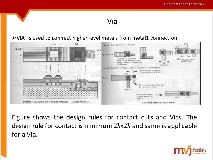
Engineered for for. Tomorrow Via ØVIA is used to connect higher level metals from metal 1 connection. Figure shows the design rules for contact cuts and Vias. The design rule for contact is minimum 2λx 2λ and same is applicable for a Via.
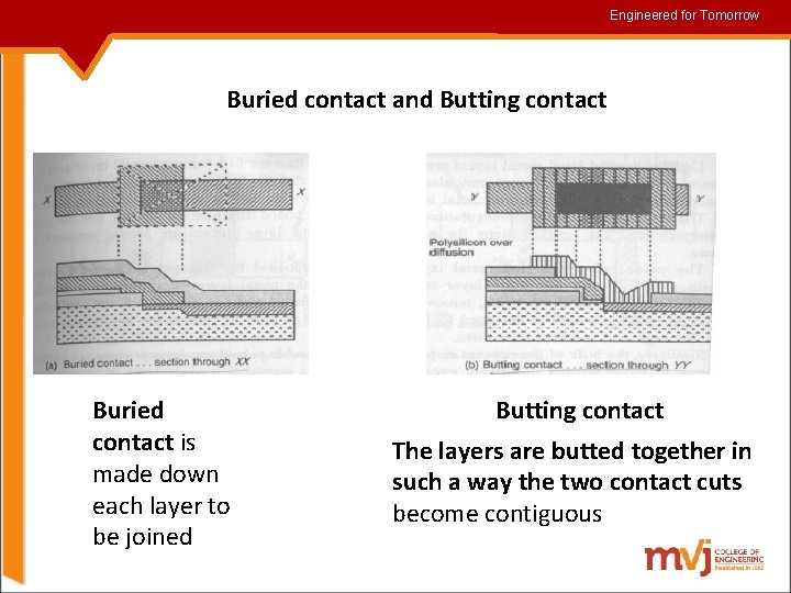
Engineered for for. Tomorrow Buried contact and Butting contact Buried contact is made down each layer to be joined Butting contact The layers are butted together in such a way the two contact cuts become contiguous
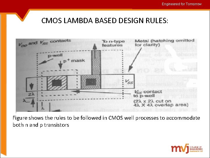
Engineered for for. Tomorrow CMOS LAMBDA BASED DESIGN RULES: Figure shows the rules to be followed in CMOS well processes to accommodate both n and p transistors
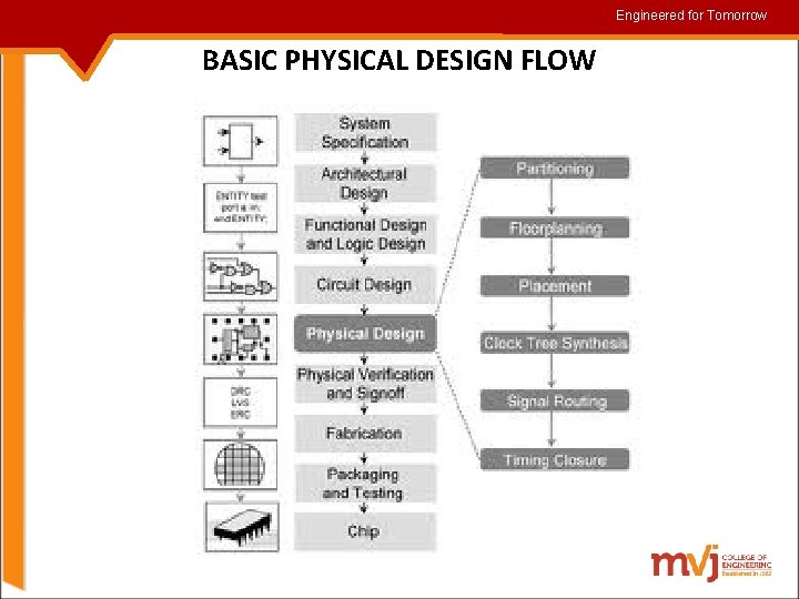
Engineered for for. Tomorrow BASIC PHYSICAL DESIGN FLOW
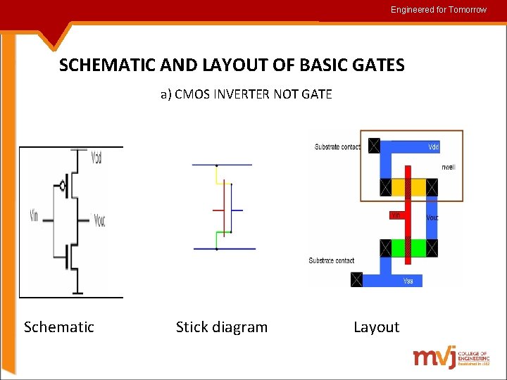
Engineered for for. Tomorrow SCHEMATIC AND LAYOUT OF BASIC GATES a) CMOS INVERTER NOT GATE Schematic Stick diagram Layout
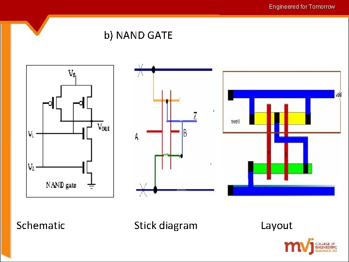
Engineered for for. Tomorrow b) NAND GATE Schematic Stick diagram Layout
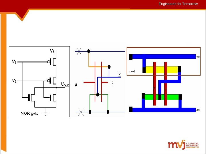
Engineered for for. Tomorrow
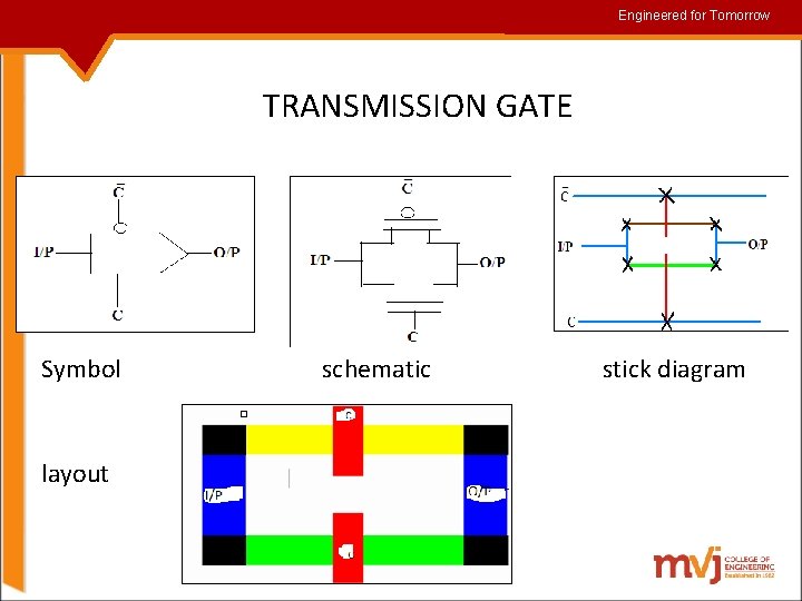
Engineered for for. Tomorrow TRANSMISSION GATE Symbol layout schematic stick diagram
- Slides: 25