Engineered for Tomorrow Subject Name Fundamentals Of CMOS
Engineered for Tomorrow Subject Name: Fundamentals Of CMOS VLSI Subject Code: 10 EC 56 Prepared By: Aswini N, Praphul M N Department: ECE Date: 10/11/2014 Engineered for Tomorrow Prepared by : MN PRAPHUL & ASWINI N Assistant professor ECE Department Date : 11/10/14
Engineered for for. Tomorrow UNIT 4 BASIC CIRCUIT DESIGN CONCEPTS
Engineered for for. Tomorrow Syllabus q. Sheet resistance q. Area capacitances q. The Delay unit q. Inverter delays q. Driving capacitive loads q. Propogation Delays q. Wiring capacitances
Engineered for for. Tomorrow Fundamental concepts that are required to estimate the performance of the system. 1. Resistance, capacitance and inductance calculations. 2. Delay estimations 3. Determination of conductor size for power and clock Distribution 4. Power consumption 5. Charge sharing 6. Design margin 7. Reliabiltiy 8. Effects and extent of scaling
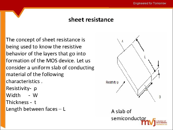
Engineered for for. Tomorrow sheet resistance The concept of sheet resistance is being used to know the resistive behavior of the layers that go into formation of the MOS device. Let us consider a uniform slab of conducting material of the following characteristics. Resistivity- ρ Width - W Thickness - t Length between faces – L A slab of semiconductor
Engineered for for. Tomorrow sheet resistance. . (cont) • Resistance is given by RAB= ρL/A Ω. • The area of the slab considered is given by A=Wt. • There fore RAB= ρL/Wt Ω. • If the slab is considered as a square then L=W. therefore RAB=ρ/t which is called as sheet resistance represented by Rs. • The unit of sheet resistance is ohm per square. Note: Rs is independent of the area of the slab. Hence we can conclude that a 1 um per side square has the same resistance as that of 1 cm per side square of the same material.
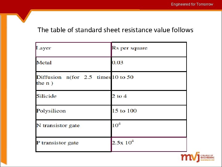
Engineered for for. Tomorrow The table of standard sheet resistance value follows
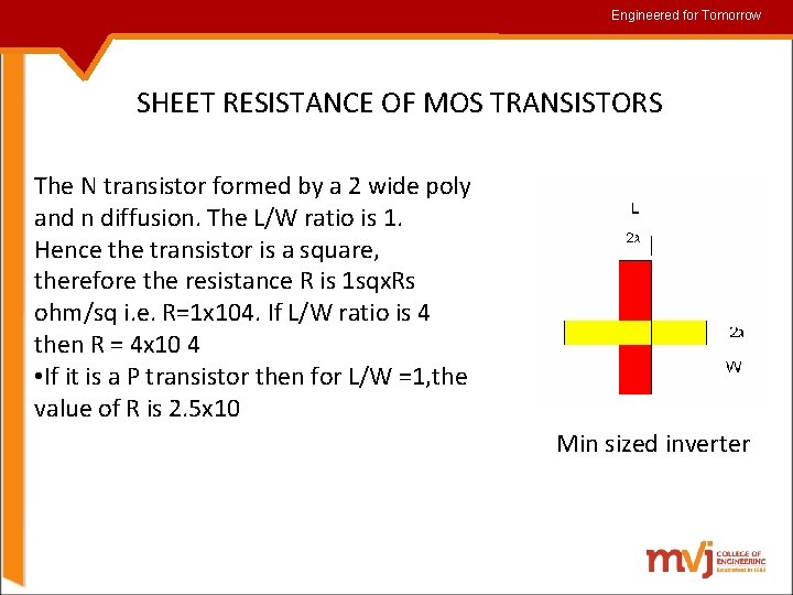
Engineered for for. Tomorrow SHEET RESISTANCE OF MOS TRANSISTORS The N transistor formed by a 2 wide poly and n diffusion. The L/W ratio is 1. Hence the transistor is a square, therefore the resistance R is 1 sqx. Rs ohm/sq i. e. R=1 x 10⁴. If L/W ratio is 4 then R = 4 x 10 4 • If it is a P transistor then for L/W =1, the value of R is 2. 5 x 10 Min sized inverter
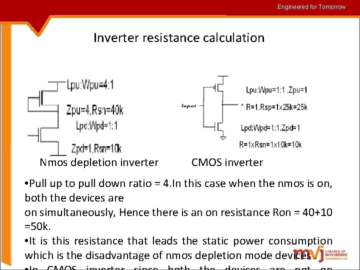
Engineered for for. Tomorrow Inverter resistance calculation Nmos depletion inverter CMOS inverter • Pull up to pull down ratio = 4. In this case when the nmos is on, both the devices are on simultaneously, Hence there is an on resistance Ron = 40+10 =50 k. • It is this resistance that leads the static power consumption which is the disadvantage of nmos depletion mode devices.
Engineered for for. Tomorrow SILICIDES • The connecting lines that run from one circuit to the other have to be optimized. For this reason the width is reduced considerably. • With the reduction is width the sheet resistance increases, increasing the RC delay component. With poly silicon the sheet resistance values vary from 15 to 100 ohm. This actually effects the extent of scaling down process. • Polysilicon is being replaced with silicide. Silicide is obtained by depositing metal on polysilicon and then sintering it. • Silicides give a sheet resistance of 2 to 4 ohm. The reduced sheet resistance makes silicides a very attractive replacement for poly silicon. But the extra processing steps is an offset to the advantage.
Engineered for for. Tomorrow Capacitance estimation 1. Gate capacitance - due to other inputs connected to output of the device. 2. Diffusion capacitance - Drain regions connected to the output. 3. Routing capacitance- due to connections between output and other inputs.
Engineered for for. Tomorrow Capacitance estimation(Cont. . ) Silicon dioxide is the insulator material used in fabrication process; knowing its thickness , the capacitance value is calculated C= eoeins. A farad D eo= permittivity of free space-8. 854 x 1014 f/cm eins= relative permitivity of sio 2=4. 0 D= thickness of the dioxide in cm A = area of the plate in cm 2 The standard unit is denoted by ロCg. It represents the capacitance between gate to channel with W=L=min feature size.
Engineered for for. Tomorrow Total gate capacitance 1. Cgd, Cgs = gate to channel capacitance lumped at the source and drain 2. Csb, Cdb = source and drain diffusion capacitance to substrate 3. Cgb = gate to bulk capacitance Total gate capacitance Cg = Cgd+Cgs+Cgb
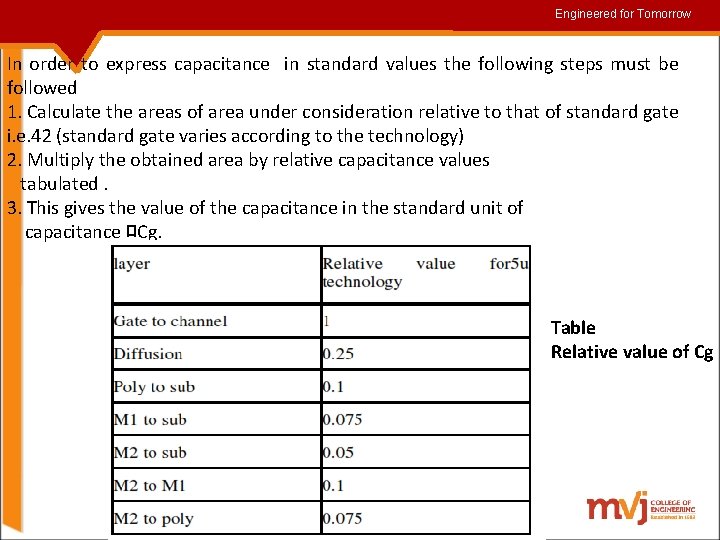
Engineered for for. Tomorrow In order to express capacitance in standard values the following steps must be followed 1. Calculate the areas of area under consideration relative to that of standard gate i. e. 42 (standard gate varies according to the technology) 2. Multiply the obtained area by relative capacitance values tabulated. 3. This gives the value of the capacitance in the standard unit of capacitance ロCg. Table Relative value of Cg
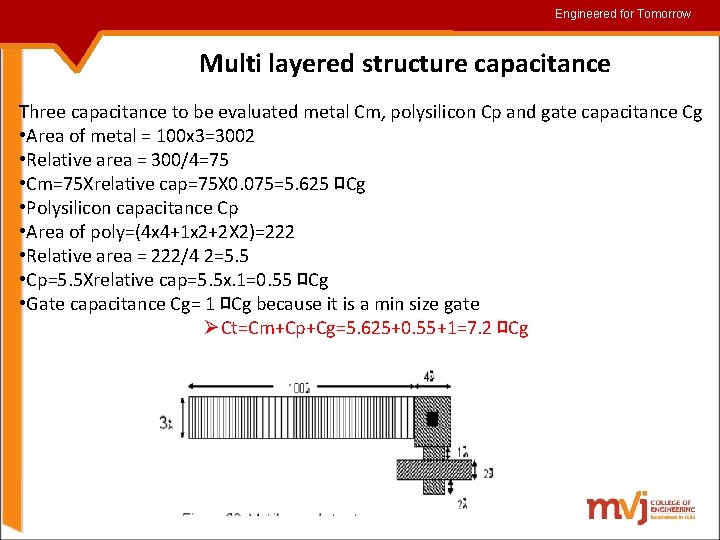
Engineered for for. Tomorrow Multi layered structure capacitance Three capacitance to be evaluated metal Cm, polysilicon Cp and gate capacitance Cg • Area of metal = 100 x 3=3002 • Relative area = 300/4=75 • Cm=75 Xrelative cap=75 X 0. 075=5. 625 ロCg • Polysilicon capacitance Cp • Area of poly=(4 x 4+1 x 2+2 X 2)=222 • Relative area = 222/4 2=5. 5 • Cp=5. 5 Xrelative cap=5. 5 x. 1=0. 55 ロCg • Gate capacitance Cg= 1 ロCg because it is a min size gate ØCt=Cm+Cp+Cg=5. 625+0. 55+1=7. 2 ロCg
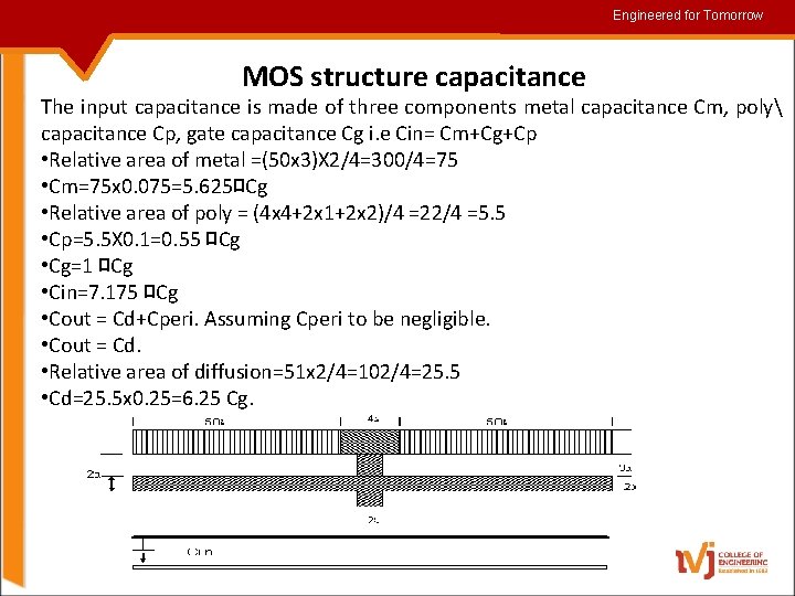
Engineered for for. Tomorrow MOS structure capacitance The input capacitance is made of three components metal capacitance Cm, poly capacitance Cp, gate capacitance Cg i. e Cin= Cm+Cg+Cp • Relative area of metal =(50 x 3)X 2/4=300/4=75 • Cm=75 x 0. 075=5. 625ロCg • Relative area of poly = (4 x 4+2 x 1+2 x 2)/4 =22/4 =5. 5 • Cp=5. 5 X 0. 1=0. 55 ロCg • Cg=1 ロCg • Cin=7. 175 ロCg • Cout = Cd+Cperi. Assuming Cperi to be negligible. • Cout = Cd. • Relative area of diffusion=51 x 2/4=102/4=25. 5 • Cd=25. 5 x 0. 25=6. 25 Cg.
Engineered for for. Tomorrow DELAY Delay can be calculated using the concept of sheet resistance and standard unit capacitance can be used to calculate the. If we consider that a one feature size poly is charged by one feature size diffusion the delay is Time constant 1= Rs (n/p channel)x 1ロCg secs. • This can be evaluated for any technology. • The value of ロCg will vary with different technologies because of the variation in the minimum feature size. • 5 u using n diffusion=104 X 0. 01=0. 1 ns safe delay 0. 03 nsec • 2 um = 104 x 0. 0032=0. 064 nsecs safe delay 0. 02 nsec • 1. 2 u= 104 x 0. 0023 = 0. 046 nsecs safe delay =0. 1 nsec
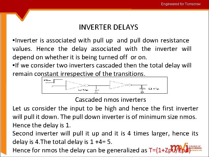
Engineered for for. Tomorrow INVERTER DELAYS • Inverter is associated with pull up and pull down resistance values. Hence the delay associated with the inverter will depend on whether it is being turned off or on. • If we consider two inverters cascaded then the total delay will remain constant irrespective of the transitions. Cascaded nmos inverters Let us consider the input to be high and hence the first inverter will pull it down. The pull down inverter is of minimum size nmos. Hence the delay is 1. Second inverter will pull it up and it is 4 times larger, hence its delay is 4. The total delay is 1 +4= 5. Hence for nmos the delay can be generalized as T=(1+Zpu/Zpd)
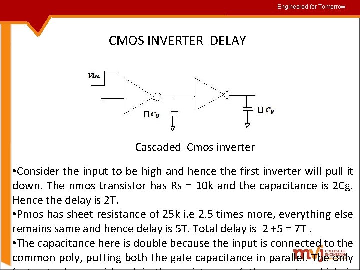
Engineered for for. Tomorrow CMOS INVERTER DELAY Cascaded Cmos inverter • Consider the input to be high and hence the first inverter will pull it down. The nmos transistor has Rs = 10 k and the capacitance is 2 Cg. Hence the delay is 2 T. • Pmos has sheet resistance of 25 k i. e 2. 5 times more, everything else remains same and hence delay is 5 T. Total delay is 2 +5 = 7 T. • The capacitance here is double because the input is connected to the common poly, putting both the gate capacitance in parallel. The only
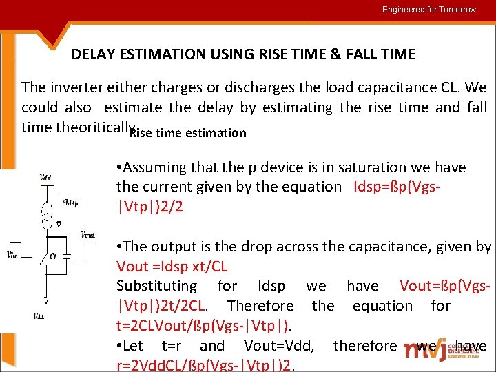
Engineered for for. Tomorrow DELAY ESTIMATION USING RISE TIME & FALL TIME The inverter either charges or discharges the load capacitance CL. We could also estimate the delay by estimating the rise time and fall time theoritically. Rise time estimation • Assuming that the p device is in saturation we have the current given by the equation Idsp=ßp(Vgs|Vtp|)2/2 • The output is the drop across the capacitance, given by Vout =Idsp xt/CL Substituting for Idsp we have Vout=ßp(Vgs|Vtp|)2 t/2 CL. Therefore the equation for t=2 CLVout/ßp(Vgs-|Vtp|). • Let t=r and Vout=Vdd, therefore we have r=2 Vdd. CL/ßp(Vgs-|Vtp|)2.
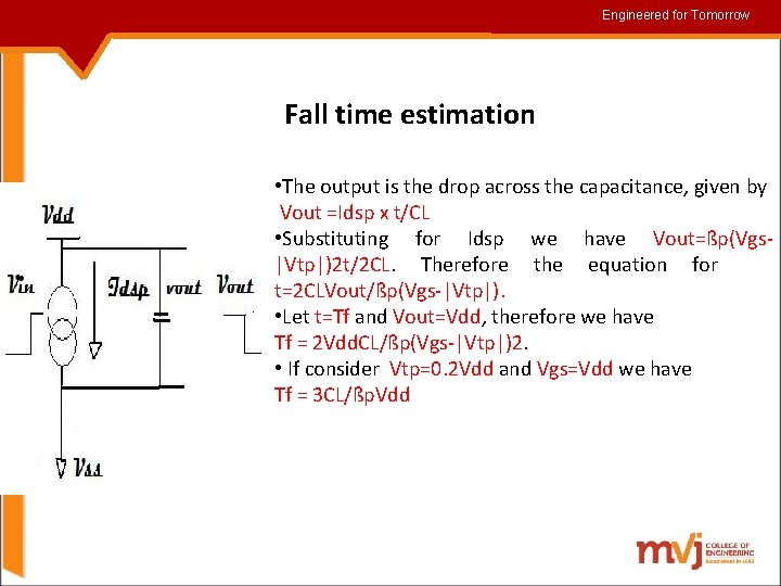
Engineered for for. Tomorrow Fall time estimation • The output is the drop across the capacitance, given by Vout =Idsp x t/CL • Substituting for Idsp we have Vout=ßp(Vgs|Vtp|)2 t/2 CL. Therefore the equation for t=2 CLVout/ßp(Vgs-|Vtp|). • Let t=Tf and Vout=Vdd, therefore we have Tf = 2 Vdd. CL/ßp(Vgs-|Vtp|)2. • If consider Vtp=0. 2 Vdd and Vgs=Vdd we have Tf = 3 CL/ßp. Vdd
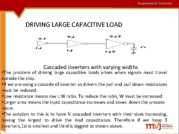
Engineered for for. Tomorrow DRIVING LARGE CAPACITIVE LOAD Cascaded inverters with varying widths • The problem of driving large capacitive loads arises when signals must travel outside the chip. • If we are using a cascade of inverter as drivers the pull and pull down resistances must be reduced. • Low résistance means low L: W ratio. To reduce the ratio, W must be increased. • Larger area means the input capacitance increases and slows down the process more. • The solution to this is to have N cascaded inverters with their sizes increasing, having the largest to drive the load capacitance. Therefore if we have 3 inverters, 1 st is smallest and third is biggest as shown above.
Engineered for for. Tomorrow DRIVING LARGE CAPACITIVE LOAD. . (cont) • Width is increasing by a factor of f towards the last stage. Now both f and N can be complementary. If f for each stage is large the number of stages N reduces but delay per stage increases. • Therefore it becomes essential to optimize. Fix N and find the minimum value of f. For nmos inverters if the input transitions from 0 to 1 the delay is f and if it transitions from 1 to 0 the delay is 4 f. • The delay for a nmos pair is 5 f. For a cmos pair it will be 7 f
Engineered for for. Tomorrow Optimum value of f. • Assume y=CL/ ロCg = f. N, therefore choice of values of N and f are interdependent. We find the value of f to minimize the delay, from the equation of y we have ln(y)=Nln(f) i. e N=ln(y)/ln(f). § If delay per stage is 5 f for nmos, then for even number of stages the total delay is N/2 5 f=2. 5 f. For cmos total delay is N/2 7 f = 3. 5 f Hence delay ά Nft=ln(y)/ln(f)ft. If f=e then N= ln(y). §The total delay is then given by 1. For N=even td=2. 5 Ne. T for nmos, td=3. 5 Ne. T for cmos 2. For N=odd transition from 0 to 1 transition from 1 to 0 td=[2. 5(N-1)+1]e. T nmos td=[2. 5(N-1)+4]e. T td=[3. 59 N-1)+2]e. T cmos td=[3. 5(N-1)+5]e T for example For N=5 which is odd we can calculate the delay fro vin=1 as td=[2. 5(5 -1)+1]e. T =11 e. T i. e. 1+4+1 = 11 e. T For vin =0 , td=[2. 5(5 -1)+4]e. T = 14 e. T 4+1+4 = 14 e. T
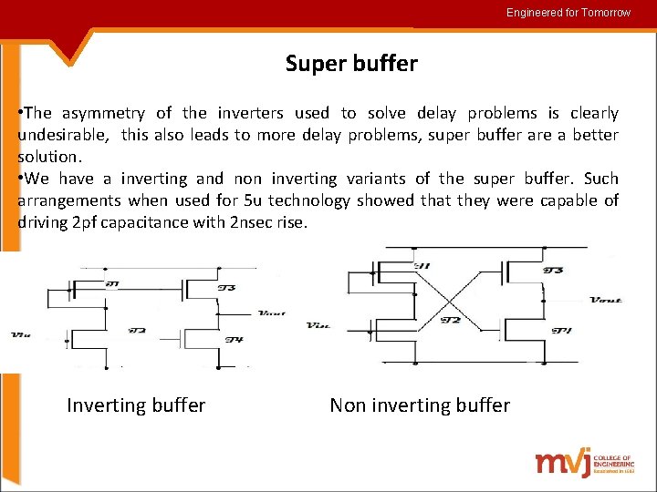
Engineered for for. Tomorrow Super buffer • The asymmetry of the inverters used to solve delay problems is clearly undesirable, this also leads to more delay problems, super buffer are a better solution. • We have a inverting and non inverting variants of the super buffer. Such arrangements when used for 5 u technology showed that they were capable of driving 2 pf capacitance with 2 nsec rise. Inverting buffer Non inverting buffer
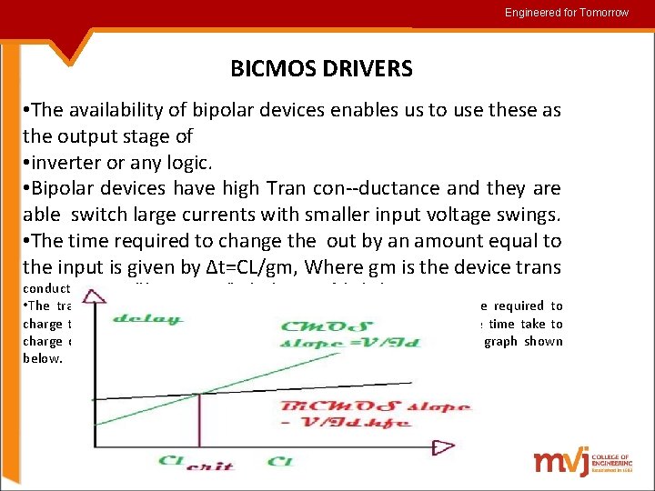
Engineered for for. Tomorrow BICMOS DRIVERS • The availability of bipolar devices enables us to use these as the output stage of • inverter or any logic. • Bipolar devices have high Tran con--ductance and they are able switch large currents with smaller input voltage swings. • The time required to change the out by an amount equal to the input is given by ∆t=CL/gm, Where gm is the device trans conductance. ∆t will be a very small value because of the high gm. • The transistor delay consists of two components Tin and TL. Tin the time required to charge the base of the transistor which is large. TL is smaller because the time take to charge capacitor is less by hfe which is the transistor gain a comparative graph shown below.
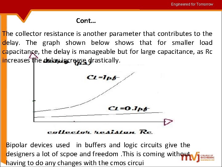
Engineered for for. Tomorrow Cont… The collector resistance is another parameter that contributes to the delay. The graph shown below shows that for smaller load capacitance, the delay is manageable but for large capacitance, as Rc increases the delay increase drastically. Bipolar devices used in buffers and logic circuits give the designers a lot of scpoe and freedom. This is coming without having to do any changes with the cmos circui
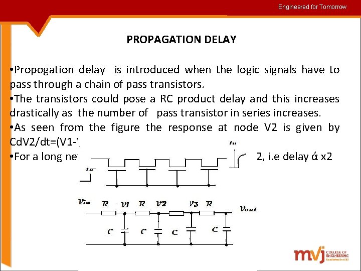
Engineered for for. Tomorrow PROPAGATION DELAY • Propogation delay is introduced when the logic signals have to pass through a chain of pass transistors. • The transistors could pose a RC product delay and this increases drastically as the number of pass transistor in series increases. • As seen from the figure the response at node V 2 is given by Cd. V 2/dt=(V 1 -V 2)(V 2 -V 3)/R • For a long network we can write RCdv/dt =dv 2/dx 2, i. e delay ά x 2
Engineered for for. Tomorrow DESIGN OF LONG POLYSILICONS The following points must be considered before going in for long wire. 1. The designer is also discouraged from designing long diffusion lines also because the capacitance is much larger. 2. When it inevitable and long poly lines have to used the best way to reduce delay is to use buffers in between. Buffers also reduce the noise sensitivity
Engineered for for. Tomorrow Wiring capacitance 1. Fringing capacitance 2. Interlayer capacitance 3. Peripheral capacitance Fringing capacitance : The major of the wiring capacitance is coming from fringing field effects. Fringing capacitances is due to parallel fine metal lines running across the chip for power conection. • The capacitance depends on the length l, thickness t and the distance d between the wire and the substrate. The accurate prediction is required for performance estimation. Hence Cw=Carea+Cff. Interlayer capacitance : It is seen when different layers cross each and hence it is neglected for simole calculations. Such capacitance can be easily estimated for regular structures and helps in modeling the circuit better.
Engineered for for. Tomorrow Peripheral capacitance : It is seen at the junction of two devices. The source and the drain n regions form junctions with the pwell (substrate) and p diffusion form with adjacent nwells leading to these side wall (peripheral) capacitance. • The capacitances are profound when the devices are shrunk in sizes and hence must be considered. Now the total diffusion capacitance is Ctotal = Carea + Cperi. • In order to reduce the side wall effects, the designers consider to use isolation regions of alternate impurity
Engineered for for. Tomorrow CHOICE OF LAYERS 1. Vdd and Vss lines must be distributed on metal lines except for some exception. 2. Long lengths of poly must be avoided because they have large Rs, it is not suitable for routing Vdd or Vss lines. 3. Since the resistance effects of the transistors are much larger, hence wiring effects due to voltage dividers are not that profound. 4. Capacitance must be accurately calculated for fast signal lines usually those using high Rs material. 5. Diffusion areas must be carefully handled because they have larger capacitance to substrate.
Engineered for for. Tomorrow SCALING OF MOS DEVICES The VLSI technology is in the process of evolution leading to reduction of the feature size and line widths. This process is called scaling down. The effect of scaling must be studied for certain parameters that effect the performance. The parameters are as stated below 1. Minimum feature size 2. Number of gates on one chip 3. Power dissipation 4. Maximum operational frequency 5. Die size 6. Production cost. These are also called as figures of merit
Engineered for for. Tomorrow Scaling models There are three types of scaling models used 1. Constant electric field scaling model. 2. Constant voltage scaling model. 3. Combined voltage and field model. The three models make use of two scaling factors 1/ß and 1/ά. 1/ß is chosen as the scaling factor for Vdd, gate oxide thickness D. 1/ ά is chosen as the scaling factor for all the linear dimensions like length, width etc. the figure next shows the dimensions and their scaling factors

Engineered for for. Tomorrow Simple derivations for scaling down the device parameters 1. Gate area Ag Ag= L x W. Since L & W are scaled down by 1/ ά. Ag is scaled down by 1/ ά. 2. Gate capacitance per unit area Co=o/D, permittivity of sio 2 cannot be scaled, hence Co can be scaled 1/1/ß=ß. 3. Gate capacitance Cg Cg=Cox. A=Cox. Lx. W. Therefore Cg can be scaled by ßx 1/ ά= ß/ ά. 4. Parasitic capacitance Cx=Ax/d, where Ax is the area of the depletion around the drain or source. d is the depletion width. Ax is scaled down by 1/ά 2 and d is scaled by 1/ά. Hence Cx is scaled by 1/ ά 2 /1/ ά = 1/ ά.
Engineered for for. Tomorrow 5. Carrier density in the channel Qon=Co. Vgs Co is scaled by ß and Vgs is scaled by 1/ ß, hence Qo is scaled by ßx 1/ß =1. 6. Channel resistance Ro Ron = L/Wx 1/Qoxµ, µ is mobility of charge carriers. Ro is scaled by 1/ά/1/ άx 1=1. 7. Gate delay Td Td is proportional to Ro and Cg. Td is scaled by 1 x ß/ά 2= ß/ά 2.
Engineered for for. Tomorrow Limitations of Scaling • Substrate doping • Depletion width • Limits of miniaturization • Limits of interconnect and contact resistance • Limits due to sub threshold currents • Limits on logic levels and supply voltage due to noise • Limits due to current density
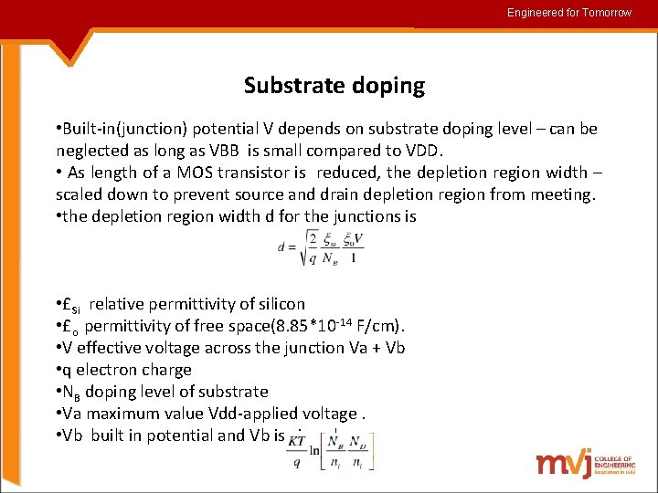
Engineered for for. Tomorrow Substrate doping • Built-in(junction) potential V depends on substrate doping level – can be neglected as long as VBB is small compared to VDD. • As length of a MOS transistor is reduced, the depletion region width – scaled down to prevent source and drain depletion region from meeting. • the depletion region width d for the junctions is • £Si relative permittivity of silicon • £o permittivity of free space(8. 85*10 -14 F/cm). • V effective voltage across the junction Va + Vb • q electron charge • NB doping level of substrate • Va maximum value Vdd-applied voltage. • Vb built in potential and Vb is given by
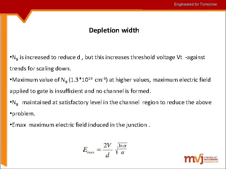
Engineered for for. Tomorrow Depletion width • NB is increased to reduce d , but this increases threshold voltage Vt -against trends for scaling down. • Maximum value of NB (1. 3*1019 cm-3) at higher values, maximum electric field applied to gate is insufficient and no channel is formed. • NB maintained at satisfactory level in the channel region to reduce the above • problem. • Emax maximum electric field induced in the junction.
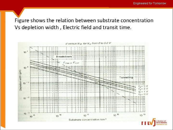
Engineered for for. Tomorrow Figure shows the relation between substrate concentration Vs depletion width , Electric field and transit time.
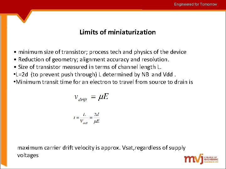
Engineered for for. Tomorrow Limits of miniaturization • minimum size of transistor; process tech and physics of the device • Reduction of geometry; alignment accuracy and resolution. • Size of transistor measured in terms of channel length L. • L=2 d (to prevent push through) L determined by NB and Vdd. • Minimum transit time for an electron to travel from source to drain is maximum carrier drift velocity is approx. Vsat, regardless of supply voltages
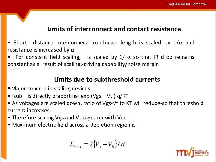
Engineered for for. Tomorrow Limits of interconnect and contact resistance • Short distance interconnect- conductor length is scaled by 1/α and resistance is increased by α • For constant field scaling, I is scaled by 1/ α so that IR drop remains constant as a result of scaling. -driving capability/noise margin. Limits due to subthreshold currents • Major concern in scaling devices. • Isub is directly praportinal exp (Vgs – Vt ) q/KT • As voltages are scaled down, ratio of Vgs-Vt to KT will reduce-so that threshold current increases. • Therefore scaling Vgs and Vt together with Vdd. • Maximum electric field across a depletion region is
Engineered for for. Tomorrow Limits on supply voltage due to noise • Decreased inter-feature spacing and greater switching speed –result in noise problems. Observations – Device scaling • Gate capacitance per micron is nearly independent of process • But ON resistance * micron improves with process • Gates get faster with scaling (good) • Dynamic power goes down with scaling (good) • Current density goes up with scaling (bad) • Velocity saturation makes lateral scaling unsustainable
Engineered for for. Tomorrow Observations – Interconnect scaling • Capacitance per micron is remaining constant About 0. 2 f. F/mm • Roughly 1/10 of gate capacitance. • Local wires are getting faster. • Not quite tracking transistor improvement. • But not a major problem. • Global wires are getting slower. • No longer possible to cross chip in one cycle.

Engineered for for. Tomorrow THANK YOU
- Slides: 45