ENGG6090 Reconfigurable Computing System Topic Review Presentation April
ENGG*6090 Reconfigurable Computing System Topic Review Presentation April 3 rd, 2006 Accelerating Wi. MAX System Designs with FPGAs [Xiaoguang (Shaw) LI][0190094] Instructor: Professor Shawki Areibi
Reviewed Papers: 1. Wi. MAX Opportunities and Challenges in a Wireless World, White Paper developed for the CDMA Development Group, July 2005. 2. IEEE 802. 16 a Standard and Wi. MAX Igniting Broadband Wireless Access, Worldwide Interoperability for Microwave Access Fourm. 3. Telephony’s Complete Guide to Wi. MAX, Wi. MAX © Telephony 2004 4. OFDM for wireless communications systems/Ramjee Prasad. , p. cm – {Artech House universal personal communications series}, ISBN 1 -58053 -796 -0 5. The principles of OFDM, RF signal processing, January 2001 6. Joaquin Garcia and Rene Cumplido, On the design of an FPGA-Based OFDM modulator for IEEE 802. 16 -2004, Proceedings of the 2005 International Conference on Reconfigurable Computing and FPGAs, Puebla City, Mexico 7. Maryse Wouters and et al. , Real Time Implementation on FPGA of an OFDM based Wireless LAN modem extended with Adaptive Loading, Imec vzw, DESICS, Kapeldreef 75, B-3001 Heverlee, Belgium. 8. Accelerating Wi. MAX System Design with FPGAs, White Paper, Altera, Oct. 2004 9. http: //www. xilinx. com/esp/wireless/bfwa/ieee_802_16. htm 10. Kwang-Cheng Chen et al. , A Programmable Architecture for OFDM-CDMA, IEEE Communications Maganine, Nov. 1999 2
Outline • Introduction • Wi. MAX and OFDM • FPGA-based Wi. MAX system designs • Design Challenges/Objectives • Wi. MAX solutions with Xilinx FPGAs • Wi. MAX solutions with Altera FPGAs • A real design of an FPGA-Based OFDM modulator • Results • Conclusion 3
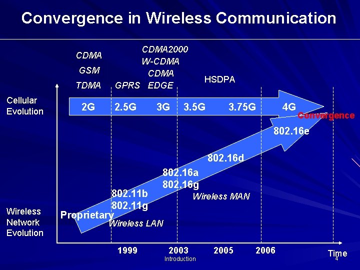
Convergence in Wireless Communication CDMA GSM TDMA Cellular Evolution 2 G CDMA 2000 W-CDMA GPRS EDGE 2. 5 G 3 G HSDPA 3. 5 G 3. 75 G 4 G Convergence 802. 16 d Wireless Network Evolution 802. 11 b 802. 11 g Proprietary 802. 16 a 802. 16 g Wireless MAN Wireless LAN 1999 2003 Introduction 2005 2006 Time 4
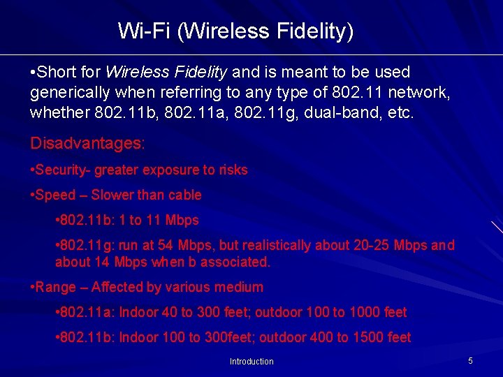
Wi-Fi (Wireless Fidelity) • Short for Wireless Fidelity and is meant to be used generically when referring to any type of 802. 11 network, whether 802. 11 b, 802. 11 a, 802. 11 g, dual-band, etc. Disadvantages: • Security- greater exposure to risks • Speed – Slower than cable • 802. 11 b: 1 to 11 Mbps • 802. 11 g: run at 54 Mbps, but realistically about 20 -25 Mbps and about 14 Mbps when b associated. • Range – Affected by various medium • 802. 11 a: Indoor 40 to 300 feet; outdoor 100 to 1000 feet • 802. 11 b: Indoor 100 to 300 feet; outdoor 400 to 1500 feet Introduction 5
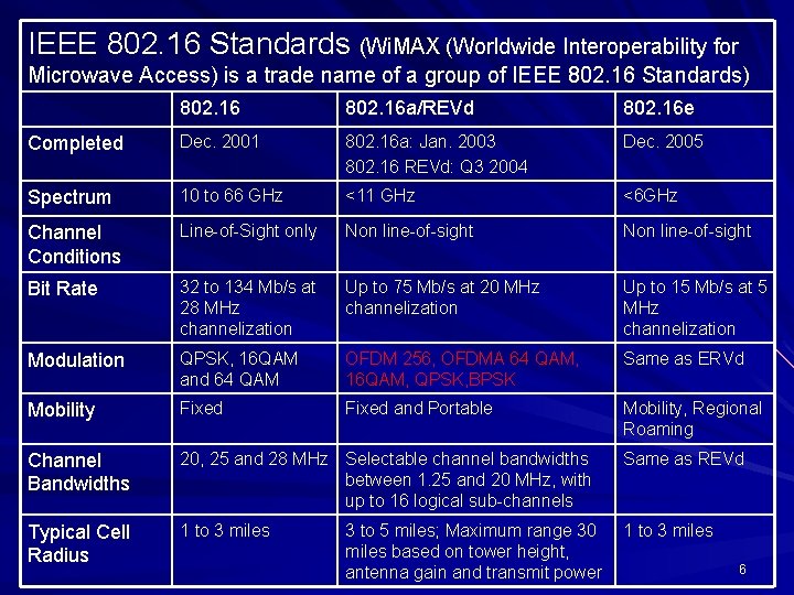
IEEE 802. 16 Standards (Wi. MAX (Worldwide Interoperability for Microwave Access) is a trade name of a group of IEEE 802. 16 Standards) 802. 16 a/REVd 802. 16 e Completed Dec. 2001 802. 16 a: Jan. 2003 802. 16 REVd: Q 3 2004 Dec. 2005 Spectrum 10 to 66 GHz <11 GHz <6 GHz Channel Conditions Line-of-Sight only Non line-of-sight Bit Rate 32 to 134 Mb/s at 28 MHz channelization Up to 75 Mb/s at 20 MHz channelization Up to 15 Mb/s at 5 MHz channelization Modulation QPSK, 16 QAM and 64 QAM OFDM 256, OFDMA 64 QAM, 16 QAM, QPSK, BPSK Same as ERVd Mobility Fixed and Portable Mobility, Regional Roaming Channel Bandwidths 20, 25 and 28 MHz Selectable channel bandwidths between 1. 25 and 20 MHz, with up to 16 logical sub-channels Same as REVd Typical Cell Radius 1 to 3 miles 3 to 5 miles; Maximum range 30 miles based on tower height, antenna gain and transmit power 6
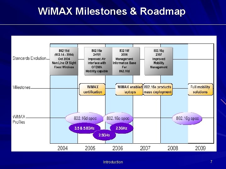
Wi. MAX Milestones & Roadmap Introduction 7
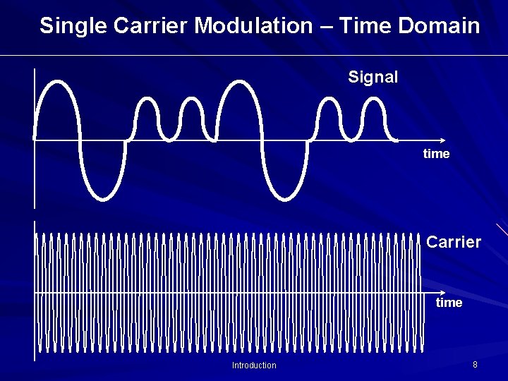
Single Carrier Modulation – Time Domain Signal time Carrier time Introduction 8
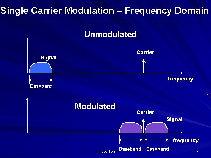
Single Carrier Modulation – Frequency Domain Unmodulated Carrier Signal frequency Baseband Modulated Carrier Signal frequency Introduction Baseband 9
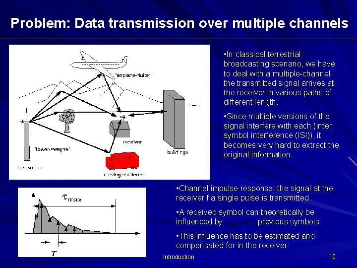
Problem: Data transmission over multiple channels • In classical terrestrial broadcasting scenario, we have to deal with a multiple-channel: the transmitted signal arrives at the receiver in various paths of different length. • Since multiple versions of the signal interfere with each (inter symbol interference (ISI)), it becomes very hard to extract the original information. • Channel impulse response: the signal at the receiver f a single pulse is transmitted. • A received symbol can theoretically be influenced by previous symbols. • This influence has to be estimated and compensated for in the receiver. Introduction 10
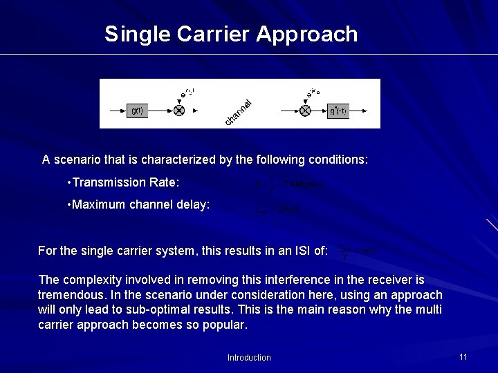
Single Carrier Approach A scenario that is characterized by the following conditions: • Transmission Rate: • Maximum channel delay: For the single carrier system, this results in an ISI of: The complexity involved in removing this interference in the receiver is tremendous. In the scenario under consideration here, using an approach will only lead to sub-optimal results. This is the main reason why the multi carrier approach becomes so popular. Introduction 11
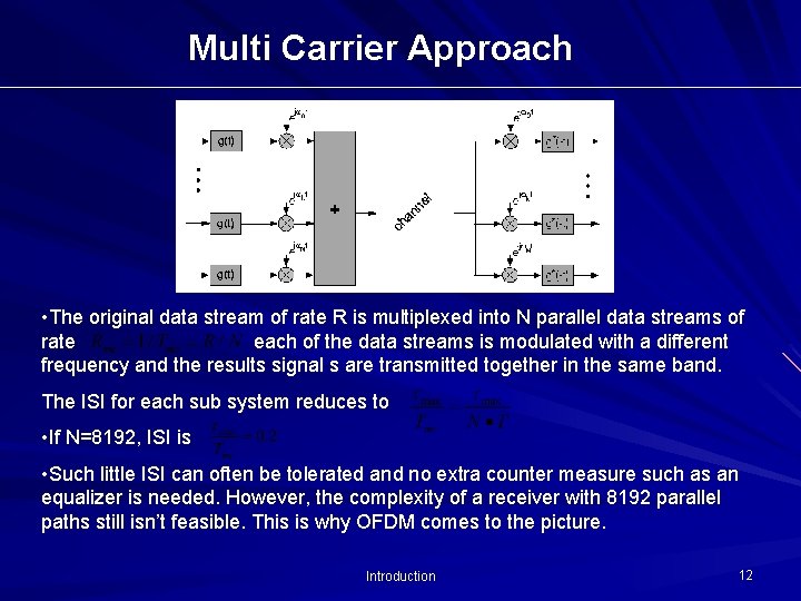
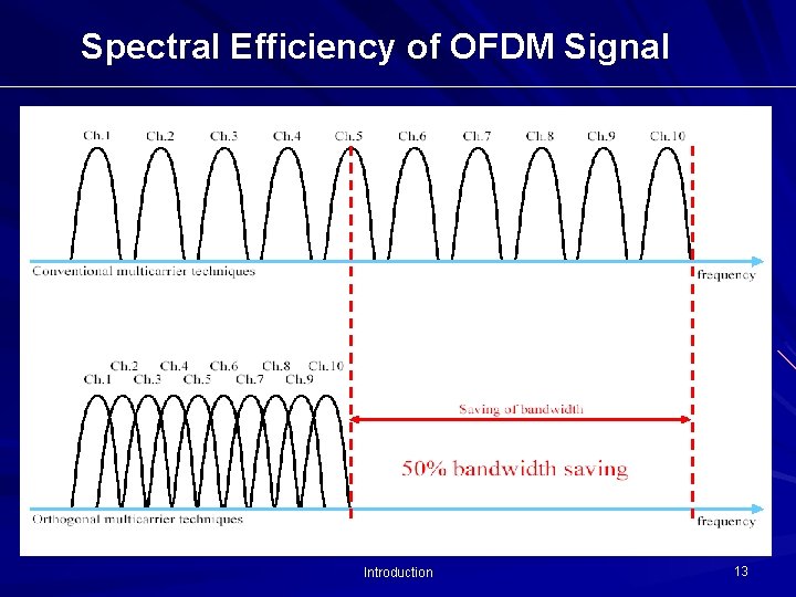
Multi Carrier Approach • The original data stream of rate R is multiplexed into N parallel data streams of rate each of the data streams is modulated with a different frequency and the results signal s are transmitted together in the same band. The ISI for each sub system reduces to • If N=8192, ISI is • Such little ISI can often be tolerated and no extra counter measure such as an equalizer is needed. However, the complexity of a receiver with 8192 parallel paths still isn’t feasible. This is why OFDM comes to the picture. Introduction 12
Spectral Efficiency of OFDM Signal Introduction 13
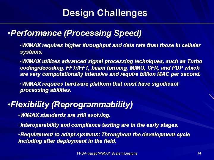
Design Challenges • Performance (Processing Speed) • Wi. MAX requires higher throughput and data rate than those in cellular systems. • Wi. MAX utilizes advanced signal processing techniques, such as Turbo coding/decoding, FFT/IFFT, beam forming, MIMO, CFR, and PDP which are very computationally intensive and require billion MAC per second. • Wi. MAX requires hardware platform that must have significant processing abilities. • Flexibility (Reprogrammability) • Wi. MAX standards are still evolving. • Interoperability and compliance testing are in the early stages. • Requirement to adapt systems: Throughout the development cycle including after deployment in the field. FPGA-based Wi. MAX System Designs 14
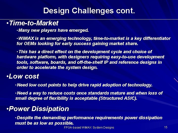
Design Challenges cont. • Time-to-Market • Many new players have emerged. • Wi. MAX is an emerging technology, time-to-market is a key differentiator for OEMs looking for early success gaining market share. • This has a direct effect on the development cycle and choice of hardware platform, with designers requiring easy-to-use development tools, software, boards, and off-the-shelf IP and reference designs in order to accelerate the system design. • Low cost • Need low cost points to help drive rapid adoption of technology. • Need a way to reduce costs once standards mature and when loss of small degree of flexibility is acceptable (Structured ASIC). • Power Dissipation • Despite the demanding performance requirements power dissipation must be as low as possible. FPGA-based Wi. MAX System Designs 15
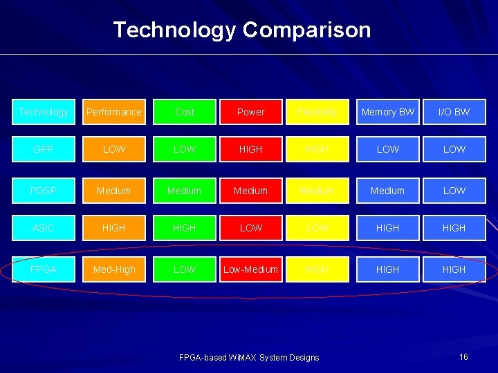
Technology Comparison Technology Performance Cost Power Flexibility Memory BW I/O BW GPP LOW HIGH LOW PDSP Medium Medium LOW ASIC HIGH LOW HIGH FPGA Med-High LOW Low-Medium HIGH FPGA-based Wi. MAX System Designs 16
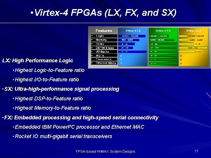
• Virtex-4 FPGAs (LX, FX, and SX) LX: High Performance Logic • Highest Logic-to-Feature ratio • Highest I/O-to-Feature ratio • SX: Ultra-high-performance signal processing • Highest DSP-to-Feature ratio • Highest Memory-to-Feature ratio • FX: Embedded processing and high-speed serial connectivity • Embedded IBM Power. PC processor and Ethernet MAC • Rocket IO multi-gigabit serial transceivers FPGA-based Wi. MAX System Designs 17
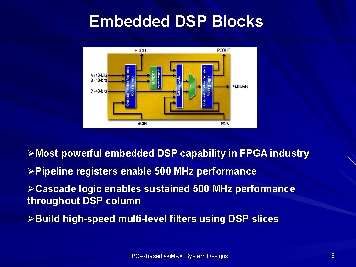
Embedded DSP Blocks ØMost powerful embedded DSP capability in FPGA industry ØPipeline registers enable 500 MHz performance ØCascade logic enables sustained 500 MHz performance throughout DSP column ØBuild high-speed multi-level filters using DSP slices FPGA-based Wi. MAX System Designs 18
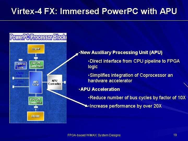
Virtex-4 FX: Immersed Power. PC with APU • New Auxiliary Processing Unit (APU) • Direct interface from CPU pipeline to FPGA logic • Simplifies integration of Coprocessor an hardware accelerator • APU Acceleration • Reduce number of bus cycles by factor of 10 X • Increase performance by over 20 X FPGA-based Wi. MAX System Designs 19
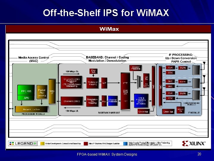
Off-the-Shelf IPS for Wi. MAX FPGA-based Wi. MAX System Designs 20
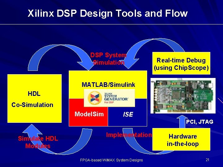
Xilinx DSP Design Tools and Flow DSP System Simulation Real-time Debug (using Chip. Scope) MATLAB/Simulink HDL Co-Simulation Model. Sim ISE PCI, JTAG Simulate HDL Modules Implementation FPGA-based Wi. MAX System Designs Hardware in-the-loop 21
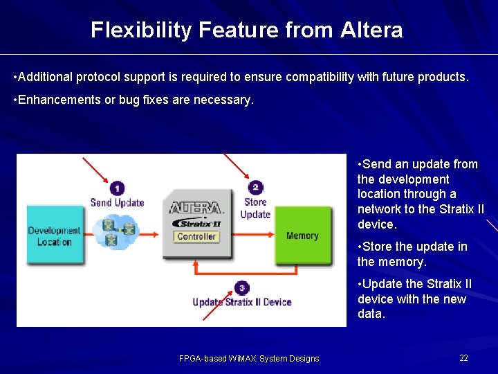
Flexibility Feature from Altera • Additional protocol support is required to ensure compatibility with future products. • Enhancements or bug fixes are necessary. • Send an update from the development location through a network to the Stratix II device. • Store the update in the memory. • Update the Stratix II device with the new data. FPGA-based Wi. MAX System Designs 22
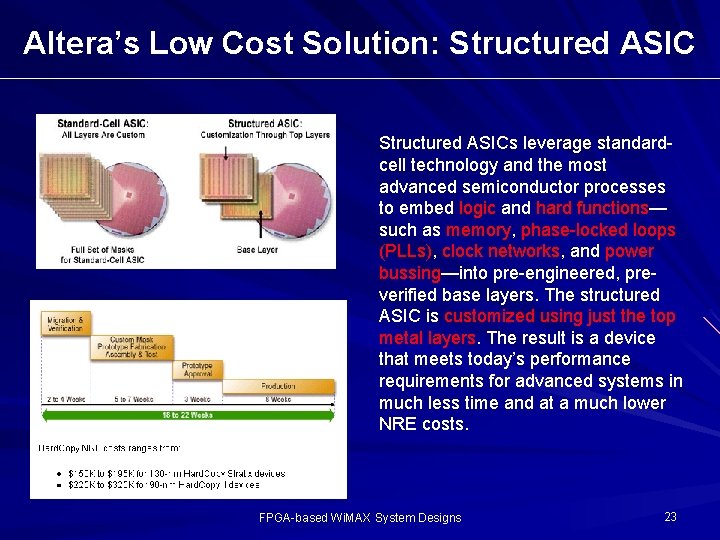
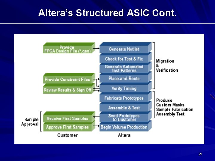
Altera’s Low Cost Solution: Structured ASICs leverage standardcell technology and the most advanced semiconductor processes to embed logic and hard functions— such as memory, phase-locked loops (PLLs), clock networks, and power bussing—into pre-engineered, preverified base layers. The structured ASIC is customized using just the top metal layers. The result is a device that meets today’s performance requirements for advanced systems in much less time and at a much lower NRE costs. FPGA-based Wi. MAX System Designs 23
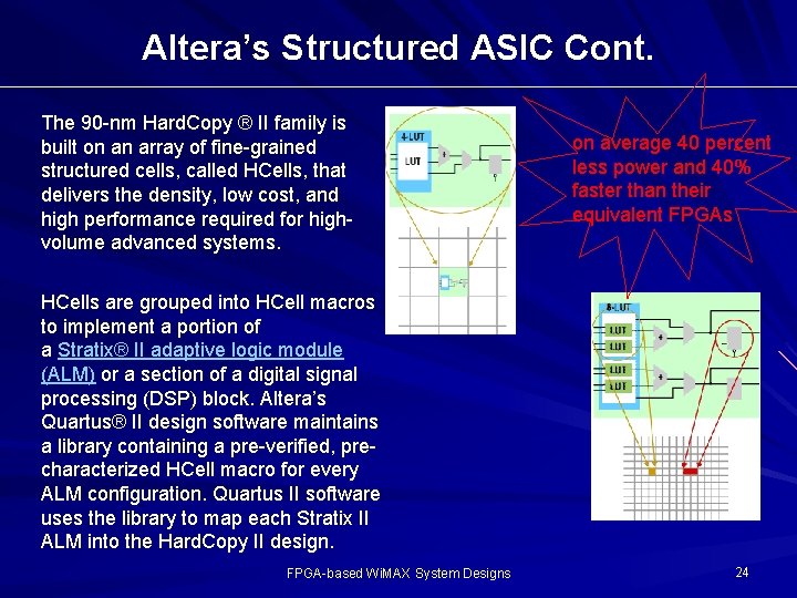
Altera’s Structured ASIC Cont. The 90 -nm Hard. Copy ® II family is built on an array of fine-grained structured cells, called HCells, that delivers the density, low cost, and high performance required for highvolume advanced systems. on average 40 percent less power and 40% faster than their equivalent FPGAs HCells are grouped into HCell macros to implement a portion of a Stratix® II adaptive logic module (ALM) or a section of a digital signal processing (DSP) block. Altera’s Quartus® II design software maintains a library containing a pre-verified, precharacterized HCell macro for every ALM configuration. Quartus II software uses the library to map each Stratix II ALM into the Hard. Copy II design. FPGA-based Wi. MAX System Designs 24
Altera’s Structured ASIC Cont. 25
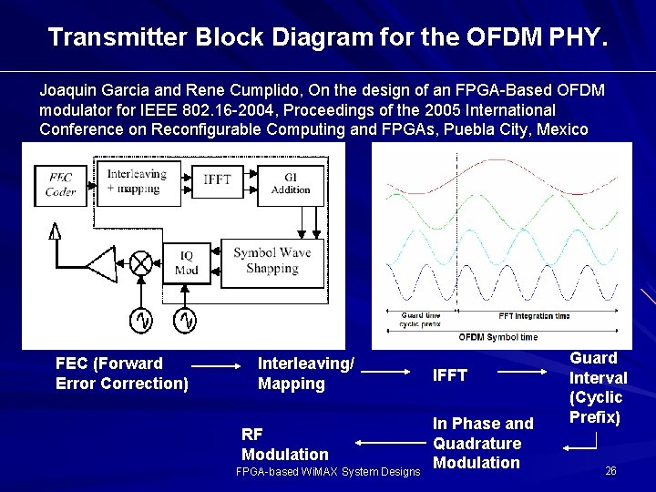
Transmitter Block Diagram for the OFDM PHY. Joaquin Garcia and Rene Cumplido, On the design of an FPGA-Based OFDM modulator for IEEE 802. 16 -2004, Proceedings of the 2005 International Conference on Reconfigurable Computing and FPGAs, Puebla City, Mexico FEC (Forward Error Correction) Interleaving/ Mapping RF Modulation FPGA-based Wi. MAX System Designs IFFT In Phase and Quadrature Modulation Guard Interval (Cyclic Prefix) 26
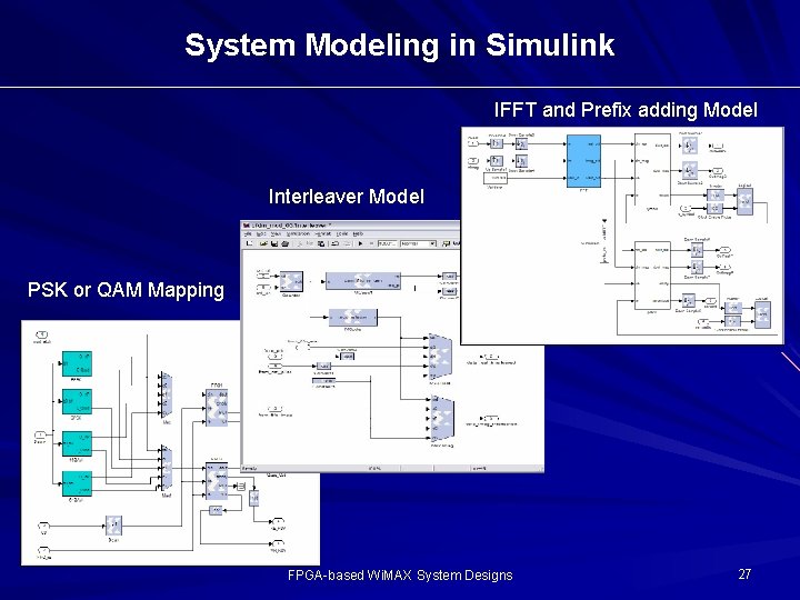
System Modeling in Simulink IFFT and Prefix adding Model Interleaver Model PSK or QAM Mapping FPGA-based Wi. MAX System Designs 27
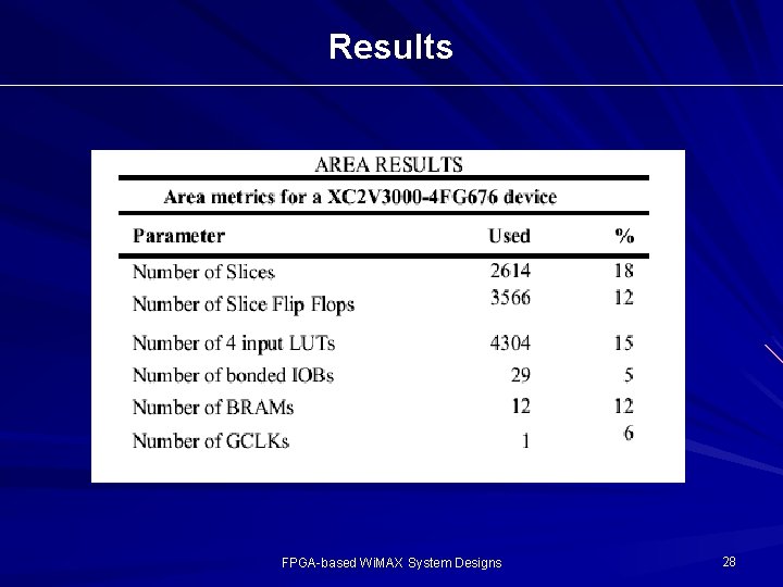
Results FPGA-based Wi. MAX System Designs 28
Conclusion • Wi. MAX is an emerging technology with significant potential and is poised to revolutionize the “broadband wireless internet access” market. • The diverse hardware requirements including processing speed, flexibility, integration and time-to market necessitate an FPGA based implementation platform. • Xilinx and Altera all provide Wi. MAX solutions including Libraries, Reference designs, and comprehensive solutions from Alliance. Core partners. Conclusion 29

30

Back up pages 31
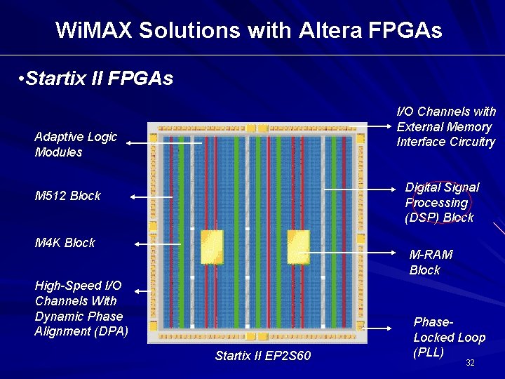
Wi. MAX Solutions with Altera FPGAs • Startix II FPGAs I/O Channels with External Memory Interface Circuitry Adaptive Logic Modules Digital Signal Processing (DSP) Block M 512 Block M 4 K Block M-RAM Block High-Speed I/O Channels With Dynamic Phase Alignment (DPA) Startix II EP 2 S 60 Phase. Locked Loop (PLL) 32
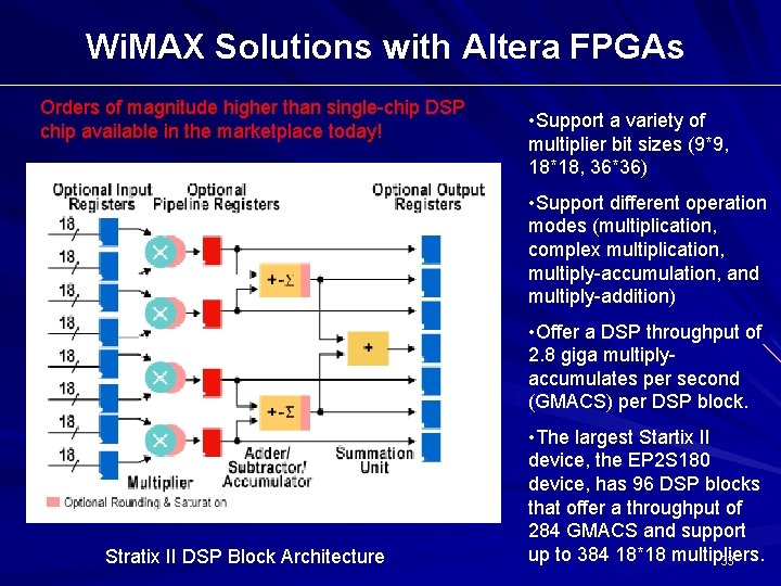
Wi. MAX Solutions with Altera FPGAs Orders of magnitude higher than single-chip DSP chip available in the marketplace today! • Support a variety of multiplier bit sizes (9*9, 18*18, 36*36) • Support different operation modes (multiplication, complex multiplication, multiply-accumulation, and multiply-addition) • Offer a DSP throughput of 2. 8 giga multiplyaccumulates per second (GMACS) per DSP block. Stratix II DSP Block Architecture • The largest Startix II device, the EP 2 S 180 device, has 96 DSP blocks that offer a throughput of 284 GMACS and support up to 384 18*18 multipliers. 33
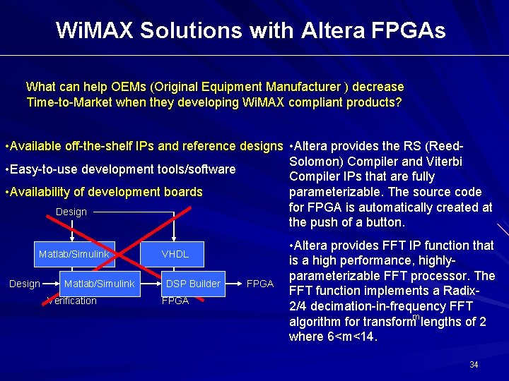
Wi. MAX Solutions with Altera FPGAs What can help OEMs (Original Equipment Manufacturer ) decrease Time-to-Market when they developing Wi. MAX compliant products? • Available off-the-shelf IPs and reference designs • Altera provides the RS (Reed. Solomon) Compiler and Viterbi • Easy-to-use development tools/software Compiler IPs that are fully • Availability of development boards parameterizable. The source code for FPGA is automatically created at Design the push of a button. Matlab/Simulink Design Matlab/Simulink Verification VHDL DSP Builder FPGA • Altera provides FFT IP function that is a high performance, highlyparameterizable FFT processor. The FFT function implements a Radix 2/4 decimation-in-frequency FFT algorithm for transformm lengths of 2 where 6<m<14. 34
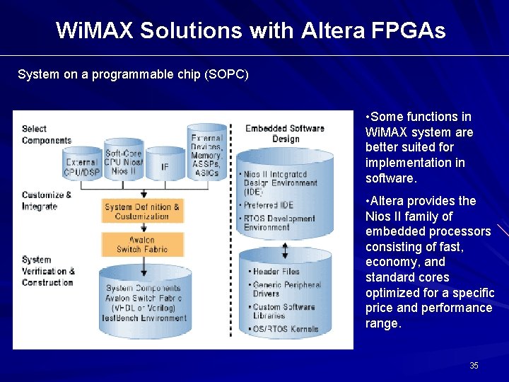
Wi. MAX Solutions with Altera FPGAs System on a programmable chip (SOPC) • Some functions in Wi. MAX system are better suited for implementation in software. • Altera provides the Nios II family of embedded processors consisting of fast, economy, and standard cores optimized for a specific price and performance range. 35
Wi. MAX Solutions with Altera FPGAs Altera’s Hard. Copy® structured ASICs are unique because they embed hard functions from the Stratix® FPGA series (and equivalent I/O) into the base layers, delivering unprecedented design flexibility. Hard. Copy devices allow you to: • Use Altera's Quartus® II software along with the EDA tools of your choice to generate your design • Test your design in-system and at-speed with a Stratix or Stratix II FPGA • Migrate seamlessly from your FPGA design to a low cost, pin-compatible Hard. Copy device with no risk and very little effort • Switch back to FPGAs if you need to change the design to accommodate a new standard, customize for a specific market or application, or if production volumes decrease 36
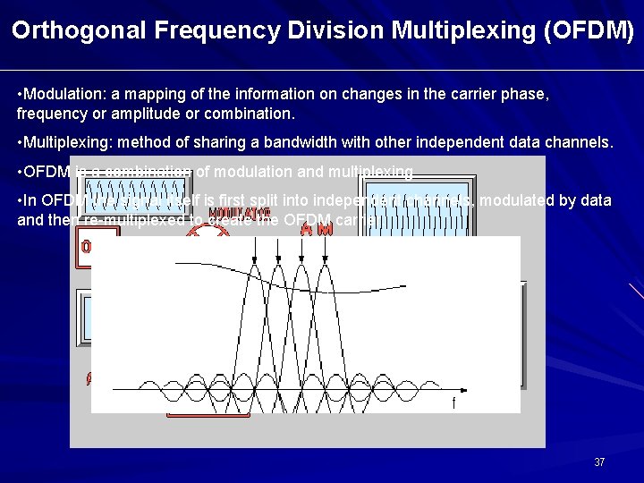
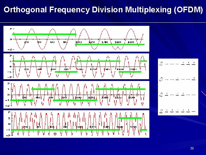
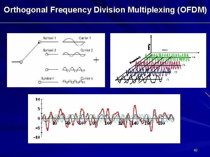
Orthogonal Frequency Division Multiplexing (OFDM) • Modulation: a mapping of the information on changes in the carrier phase, frequency or amplitude or combination. • Multiplexing: method of sharing a bandwidth with other independent data channels. • OFDM is a combination of modulation and multiplexing. • In OFDM the signal itself is first split into independent channels, modulated by data and then re-multiplexed to create the OFDM carrier. 37
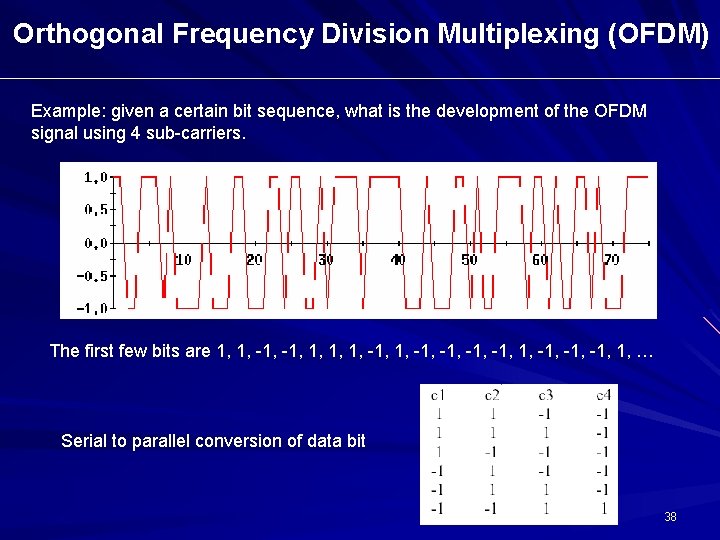
Orthogonal Frequency Division Multiplexing (OFDM) Example: given a certain bit sequence, what is the development of the OFDM signal using 4 sub-carriers. The first few bits are 1, 1, -1, 1, -1, -1, -1, 1, … Serial to parallel conversion of data bit 38
Orthogonal Frequency Division Multiplexing (OFDM) 39
Orthogonal Frequency Division Multiplexing (OFDM) 40
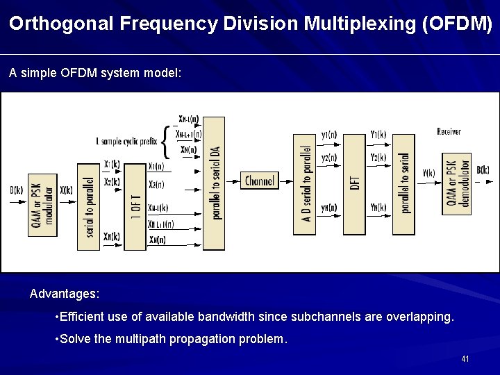
Orthogonal Frequency Division Multiplexing (OFDM) A simple OFDM system model: Advantages: • Efficient use of available bandwidth since subchannels are overlapping. • Solve the multipath propagation problem. 41
- Slides: 41