ENG 2410 Digital Design Week 9 Datapath Design





![Symbols Note memory transfers o DR M[AR] (contents of Memory) 36 Symbols Note memory transfers o DR M[AR] (contents of Memory) 36](https://slidetodoc.com/presentation_image/007b97ebeb74cadf1c78bceb2457be9d/image-36.jpg)



![Memory Transfer o Read: DR M[AR] where • • • o o M denotes Memory Transfer o Read: DR M[AR] where • • • o o M denotes](https://slidetodoc.com/presentation_image/007b97ebeb74cadf1c78bceb2457be9d/image-59.jpg)





- Slides: 88

ENG 2410 Digital Design: Week #9 “Datapath Design” S. Areibi School of Engineering University of Guelph

Week #9 Topics o Data Paths and Operations q o Register Transfer Operations q o o The Arithmetic/Logic Unit Micro-Operations Multiplexer-Based Transfer Bus-Based Transfer Complete Data Path Design Pipelining

Resources Chapter #7, Mano Sections o o o 7. 2 7. 3 7. 4 7. 5 7. 6 7. 8 Register Transfers Register Transfer Operations VHDL and RTL Micro Operations Multiplexer Based Transfers Bus Based Transfers

CPU: Main Parts

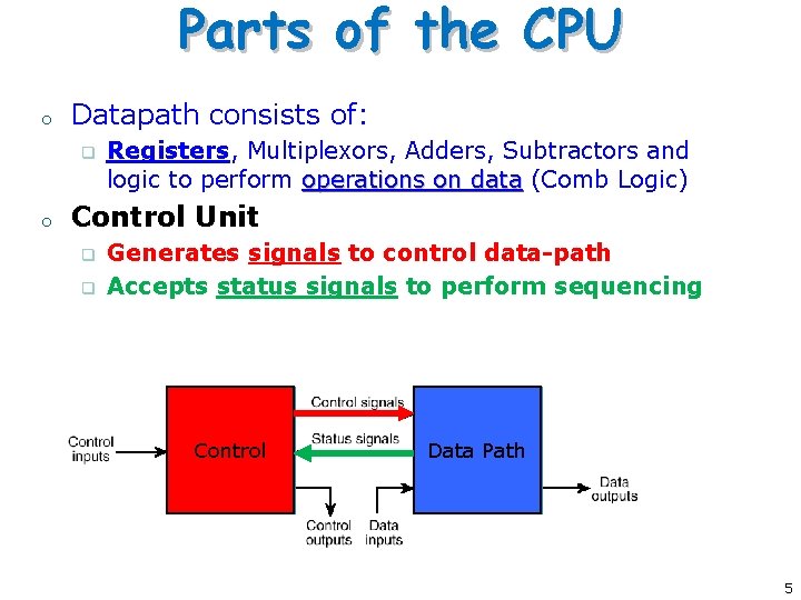
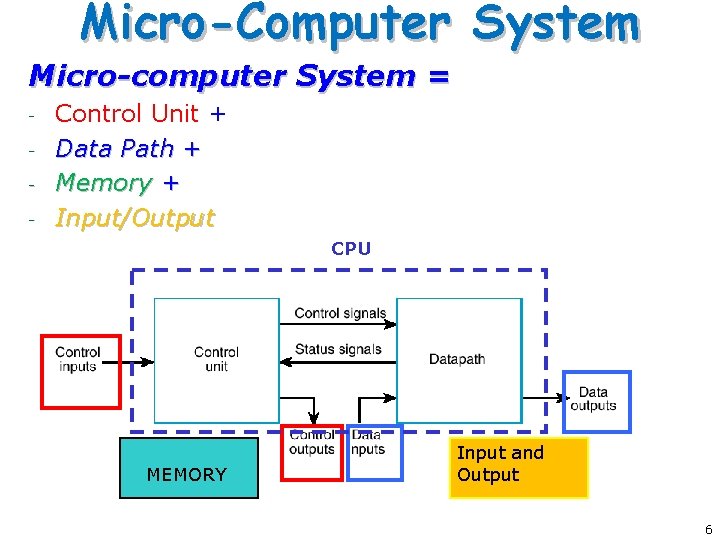
Parts of the CPU o Datapath consists of: q o Registers, Multiplexors, Adders, Subtractors and logic to perform operations on data (Comb Logic) Control Unit q q Generates signals to control data-path Accepts status signals to perform sequencing Control Data Path 5

Micro-Computer System Micro-computer System = - Control Unit + Data Path + Memory + Input/Output CPU MEMORY Input and Output 6

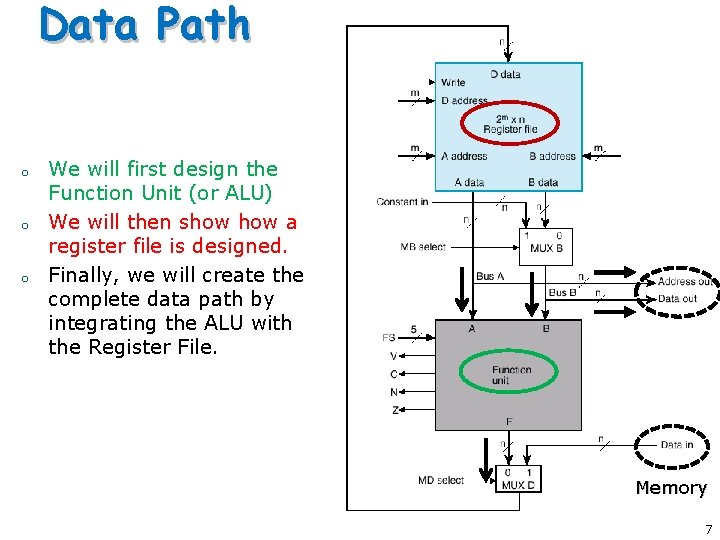
Data Path o o o We will first design the Function Unit (or ALU) We will then show a register file is designed. Finally, we will create the complete data path by integrating the ALU with the Register File. Memory 7

ALU Design

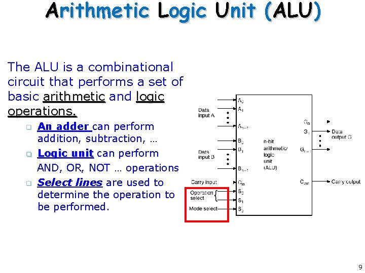
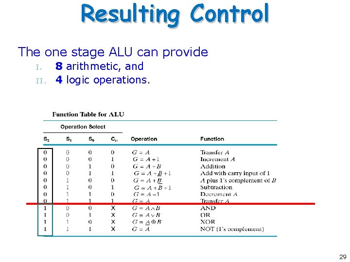
Arithmetic Logic Unit (ALU) The ALU is a combinational circuit that performs a set of basic arithmetic and logic operations. q q q An adder can perform addition, subtraction, … Logic unit can perform AND, OR, NOT … operations Select lines are used to determine the operation to be performed. 9

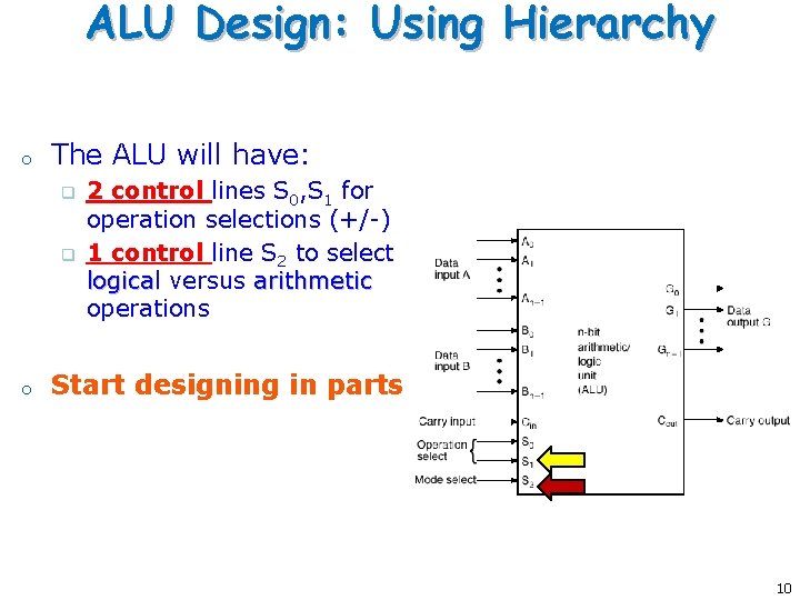
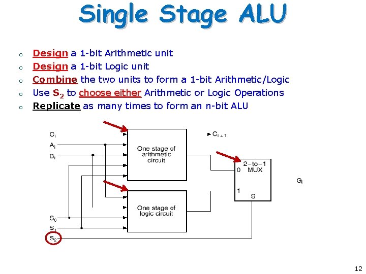
ALU Design: Using Hierarchy o The ALU will have: q q o 2 control lines S 0, S 1 for operation selections (+/-) 1 control line S 2 to select logical versus arithmetic operations Start designing in parts 10

Single Stage Design

Single Stage ALU o o o Design a 1 -bit Arithmetic unit Design a 1 -bit Logic unit Combine the two units to form a 1 -bit Arithmetic/Logic Use S 2 to choose either Arithmetic or Logic Operations Replicate as many times to form an n-bit ALU 12

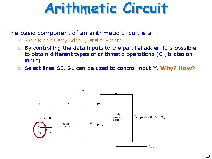
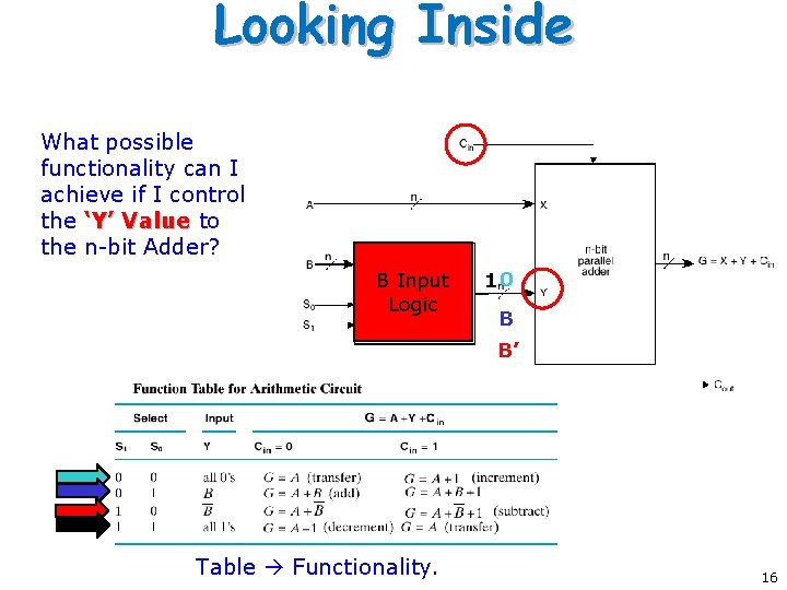
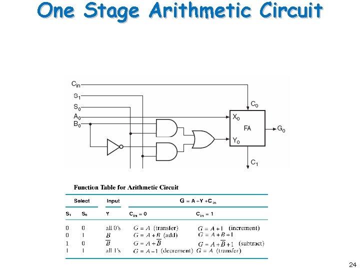
Arithmetic Circuit The basic component of an arithmetic circuit is a: ü q q N-bit Ripple Carry Adder (Parallel Adder). By controlling the data inputs to the parallel adder, it is possible to obtain different types of arithmetic operations (Cin is also an input) Select lines S 0, S 1 can be used to control input Y. Why? How? 13

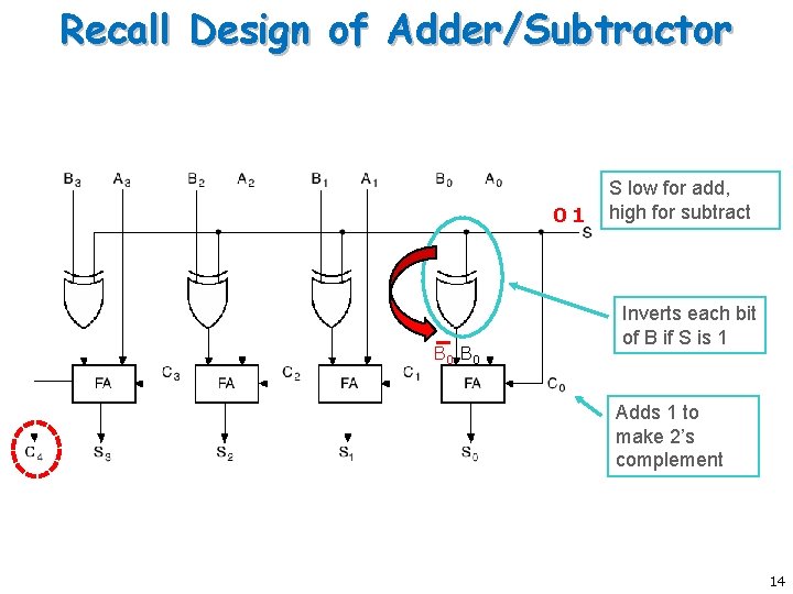
Recall Design of Adder/Subtractor 01 B 0 S low for add, high for subtract Inverts each bit of B if S is 1 Adds 1 to make 2’s complement 14

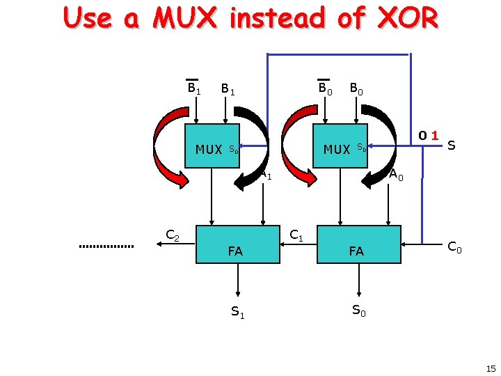
Use a MUX instead of XOR B 1 B 0 B 1 MUX B 0 MUX S 0 A 1 C 2 FA S 1 01 S 0 S A 0 C 1 FA C 0 S 0 15

Looking Inside What possible functionality can I achieve if I control the ‘Y’ Value to the n-bit Adder? B Input Logic 10 B B’ Table Functionality. 16

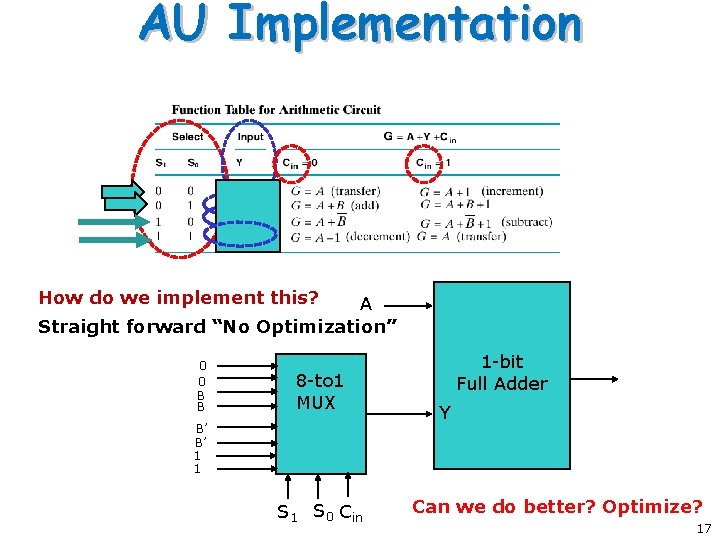
AU Implementation How do we implement this? A Straight forward “No Optimization” 0 0 B B 8 -to 1 MUX B’ B’ 1 1 S 0 Cin 1 -bit Full Adder Y Can we do better? Optimize? 17

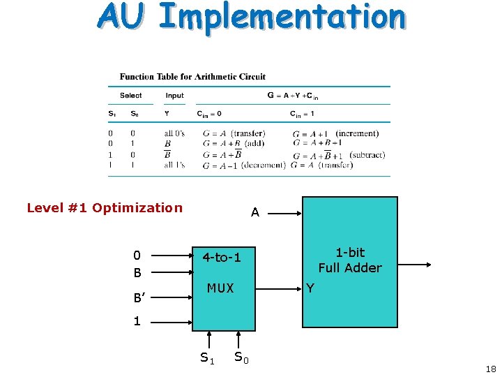
AU Implementation Level #1 Optimization 0 B B’ A 1 -bit Full Adder 4 -to-1 MUX Y 1 S 0 18

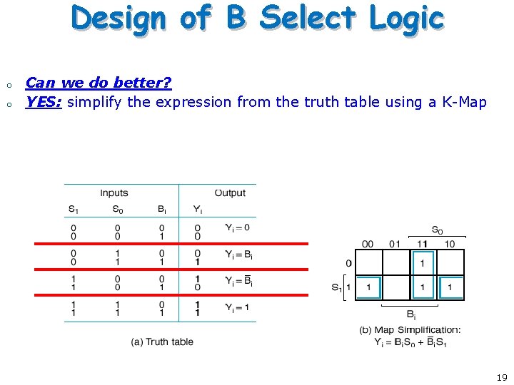
Design of B Select Logic o o Can we do better? YES: simplify the expression from the truth table using a K-Map 19

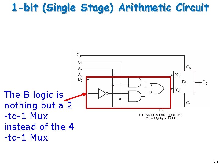
1 -bit (Single Stage) Arithmetic Circuit The B logic is nothing but a 2 -to-1 Mux instead of the 4 -to-1 Mux 20

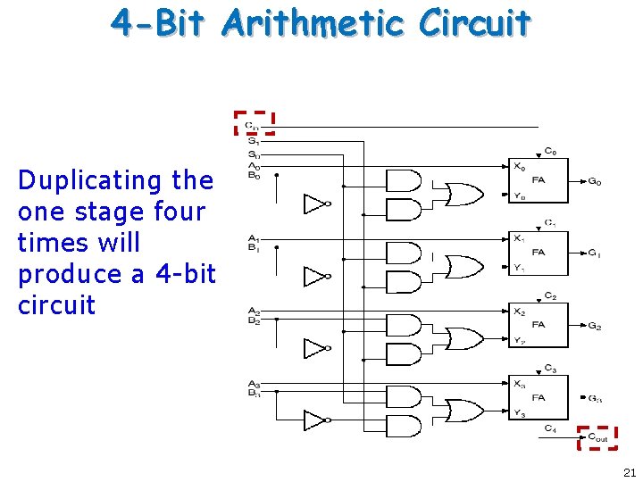
4 -Bit Arithmetic Circuit Duplicating the one stage four times will produce a 4 -bit circuit 21

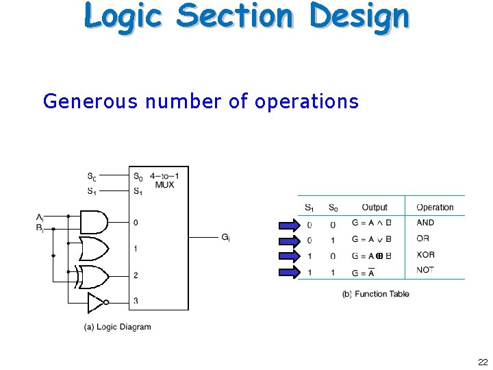
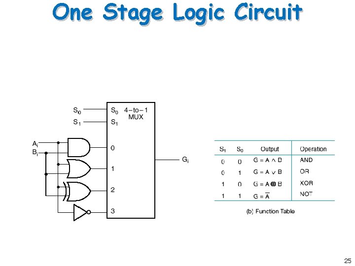
Logic Section Design Generous number of operations 22

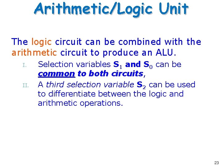
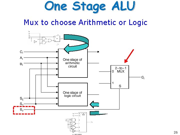
Arithmetic/Logic Unit The logic circuit can be combined with the arithmetic circuit to produce an ALU. I. II. Selection variables S 1 and S 0 can be common to both circuits, circuits A third selection variable S 2 can be used to differentiate between the logic and arithmetic operations. 23

One Stage Arithmetic Circuit 24

One Stage Logic Circuit 25

One Stage ALU Mux to choose Arithmetic or Logic 26

N-bit ALU

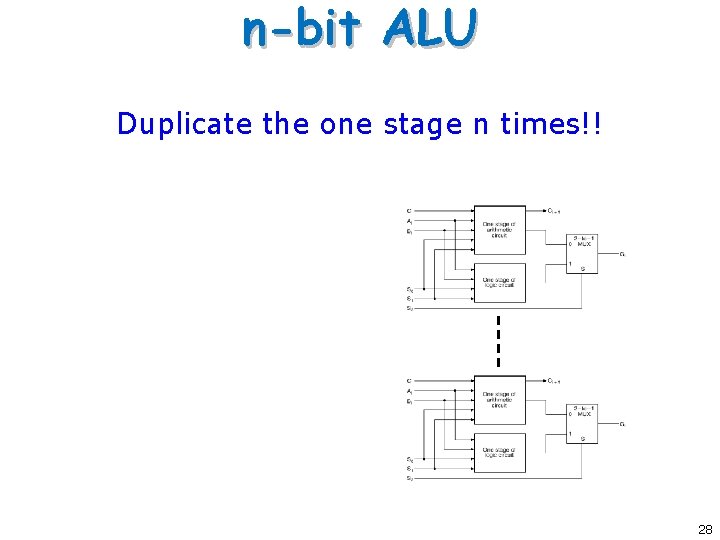
n-bit ALU Duplicate the one stage n times!! 28

Resulting Control The one stage ALU can provide I. II. 8 arithmetic, and 4 logic operations. 29

RTL

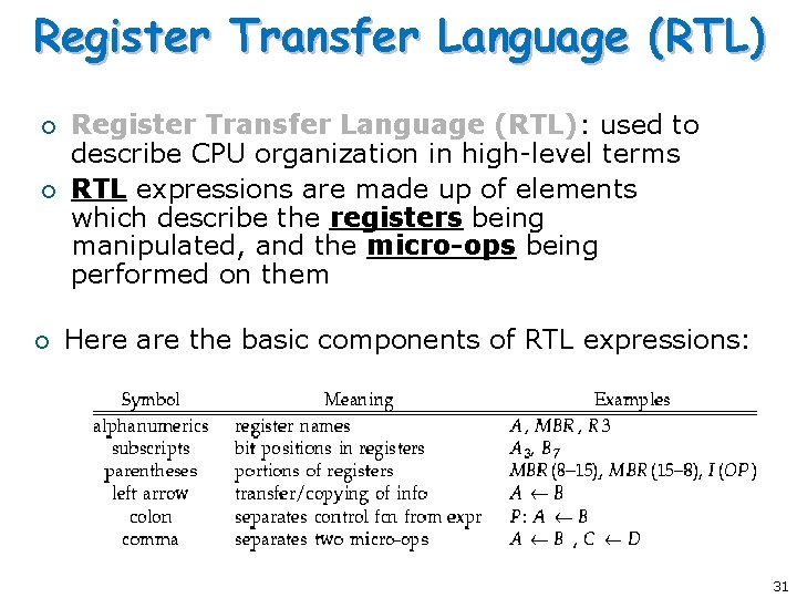
Register Transfer Language (RTL) ¡ ¡ ¡ Register Transfer Language (RTL): used to describe CPU organization in high-level terms RTL expressions are made up of elements which describe the registers being manipulated, and the micro-ops being performed on them Here are the basic components of RTL expressions: 31

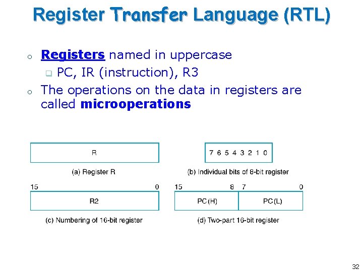
Register Transfer Language (RTL) o o Registers named in uppercase q PC, IR (instruction), R 3 The operations on the data in registers are called microoperations 32

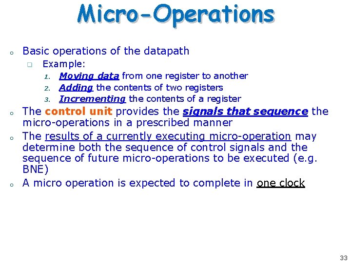
Micro-Operations o Basic operations of the datapath q Example: 1. 2. 3. o o o Moving data from one register to another Adding the contents of two registers Incrementing the contents of a register The control unit provides the signals that sequence the micro-operations in a prescribed manner The results of a currently executing micro-operation may determine both the sequence of control signals and the sequence of future micro-operations to be executed (e. g. BNE) A micro operation is expected to complete in one clock 33

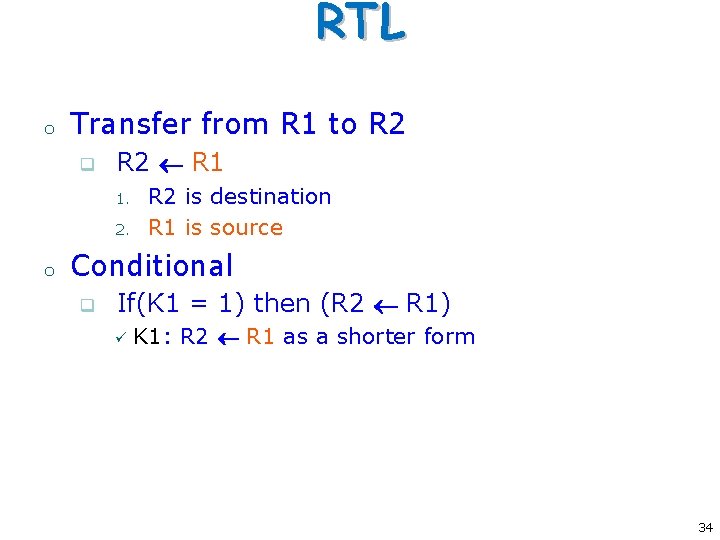
RTL o Transfer from R 1 to R 2 q R 2 R 1 1. 2. o R 2 is destination R 1 is source Conditional q If(K 1 = 1) then (R 2 R 1) ü K 1: R 2 R 1 as a shorter form 34

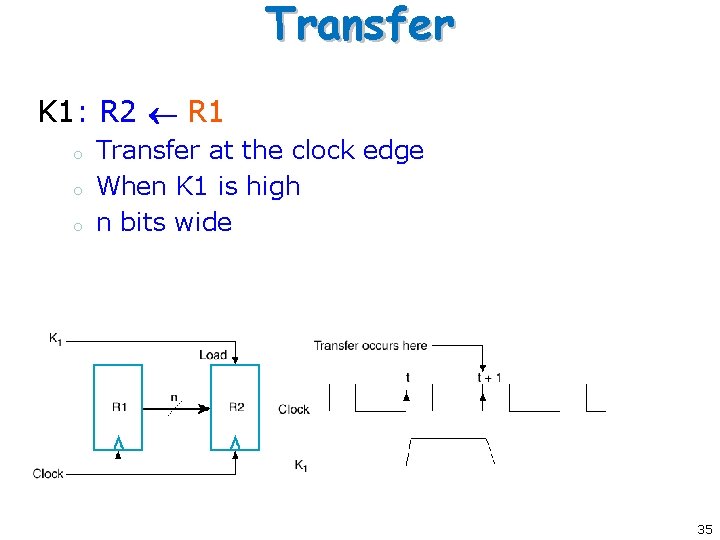
Transfer K 1: R 2 R 1 o o o Transfer at the clock edge When K 1 is high n bits wide 35
![Symbols Note memory transfers o DR MAR contents of Memory 36 Symbols Note memory transfers o DR M[AR] (contents of Memory) 36](https://slidetodoc.com/presentation_image/007b97ebeb74cadf1c78bceb2457be9d/image-36.jpg)
Symbols Note memory transfers o DR M[AR] (contents of Memory) 36

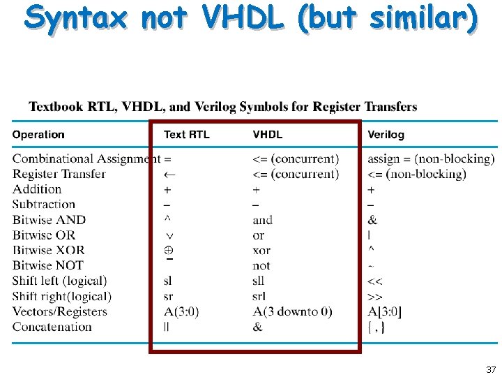
Syntax not VHDL (but similar) 37

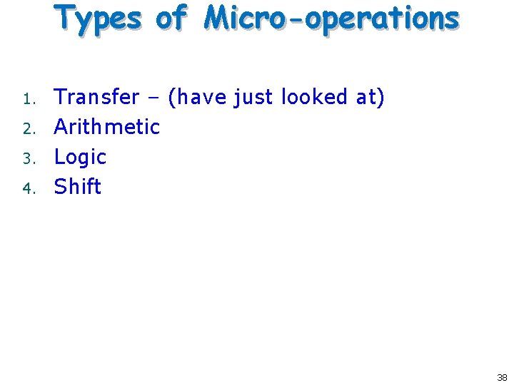
Types of Micro-operations 1. 2. 3. 4. Transfer – (have just looked at) Arithmetic Logic Shift 38

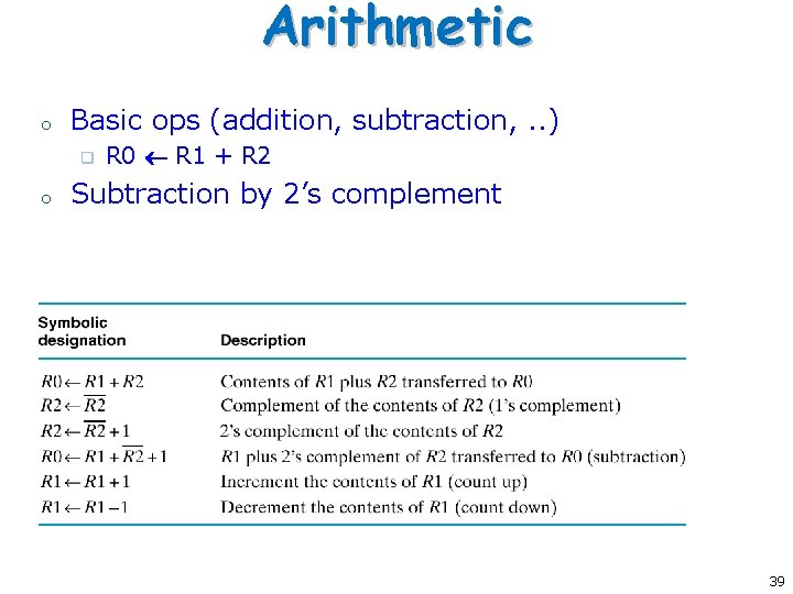
Arithmetic o Basic ops (addition, subtraction, . . ) q o R 0 R 1 + R 2 Subtraction by 2’s complement 39

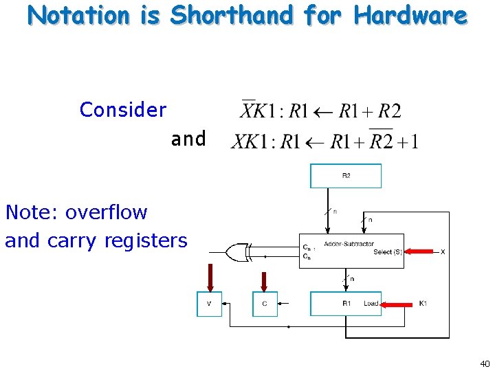
Notation is Shorthand for Hardware Consider and Note: overflow and carry registers 40

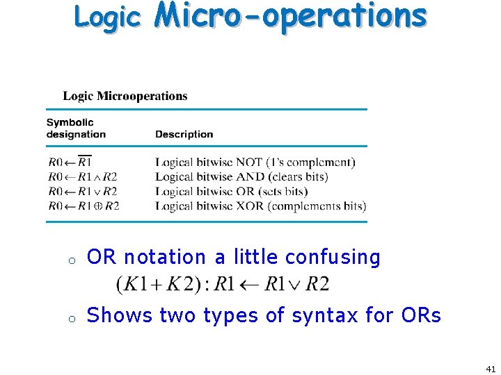
Logic Micro-operations o OR notation a little confusing o Shows two types of syntax for ORs 41

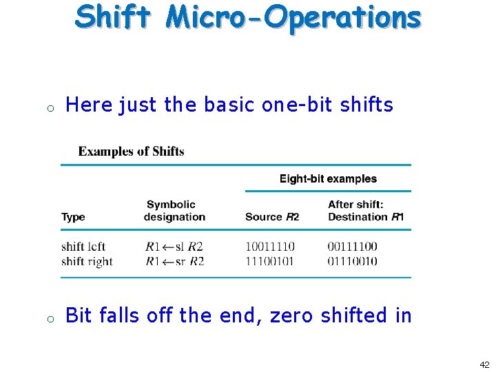
Shift Micro-Operations o Here just the basic one-bit shifts o Bit falls off the end, zero shifted in 42

Multiplexor Based Transfer

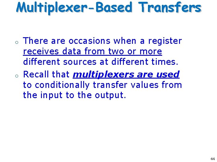
Multiplexer-Based Transfers o o There are occasions when a register receives data from two or more different sources at different times. Recall that multiplexers are used to conditionally transfer values from the input to the output. 44

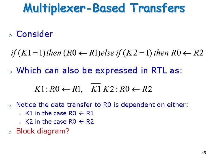
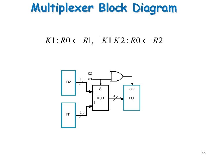
Multiplexer-Based Transfers o Consider o Which can also be expressed in RTL as: o Notice the data transfer to R 0 is dependent on either: o o o K 1 in the case R 0 R 1 K 2 in the case R 0 R 2 Block diagram? 45

Multiplexer Block Diagram 46

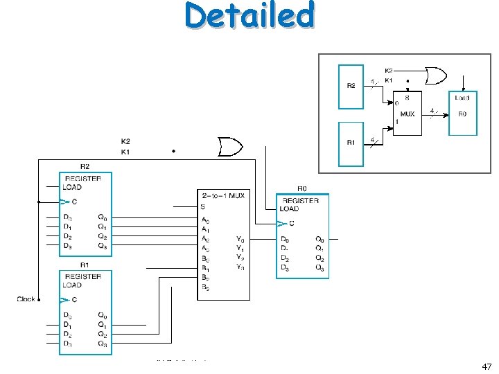
Detailed 47

Bus Based Transfer

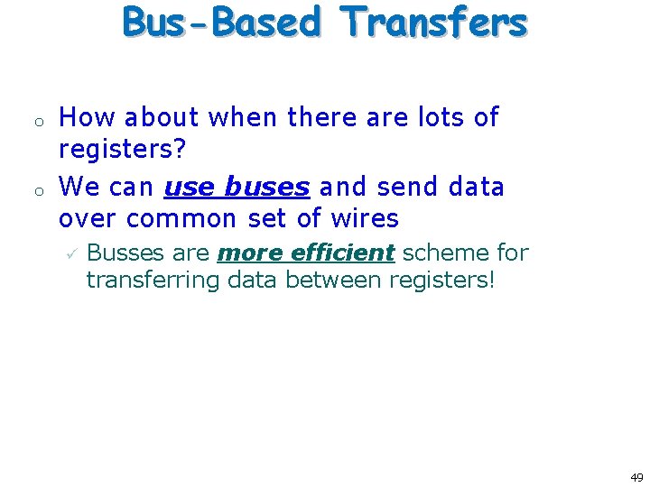
Bus-Based Transfers o o How about when there are lots of registers? We can use buses and send data over common set of wires ü Busses are more efficient scheme for transferring data between registers! 49

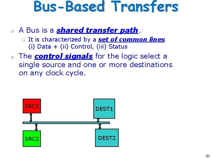
Bus-Based Transfers o A Bus is a shared transfer path. q o It is characterized by a set of common lines (i) Data + (ii) Control, (iii) Status The control signals for the logic select a single source and one or more destinations on any clock cycle. SRC 1 SRC 2 DEST 1 DEST 2 50

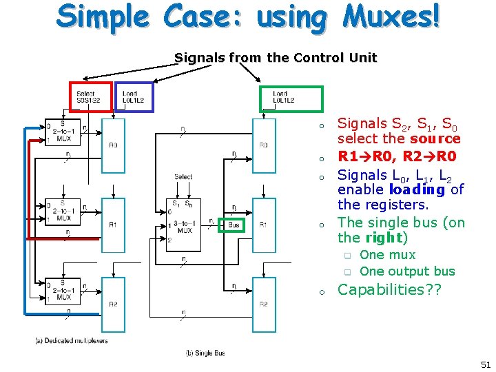
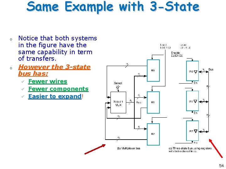
Simple Case: using Muxes! Signals from the Control Unit o o Signals S 2, S 1, S 0 select the source R 1 R 0, R 2 R 0 Signals L 0, L 1, L 2 enable loading of the registers. The single bus (on the right) q q o One mux One output bus Capabilities? ? 51

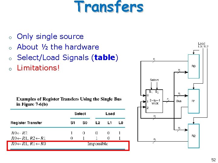
Transfers o o Only single source About ½ the hardware Select/Load Signals (table) Limitations! 52

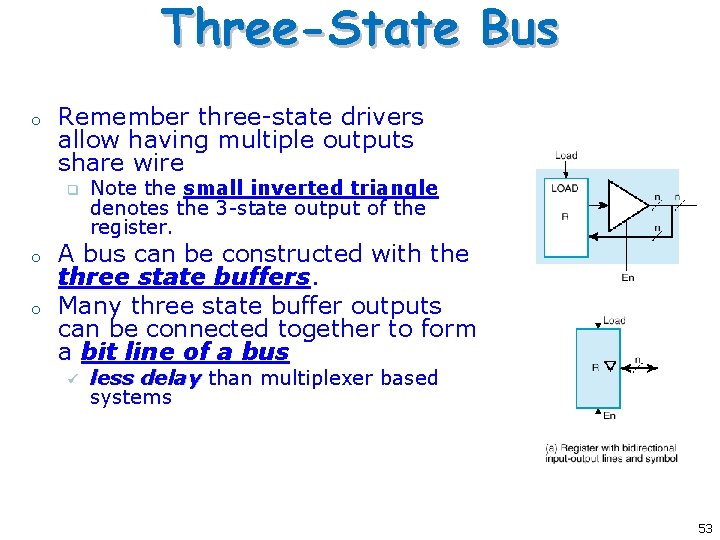
Three-State Bus o Remember three-state drivers allow having multiple outputs share wire q o o Note the small inverted triangle denotes the 3 -state output of the register. A bus can be constructed with the three state buffers. Many three state buffer outputs can be connected together to form a bit line of a bus ü less delay than multiplexer based systems 53

Same Example with 3 -State o o Notice that both systems in the figure have the same capability in term of transfers. However the 3 -state bus has: ü ü ü Fewer wires Fewer components Easier to expand! expand 54

Memory Transfer

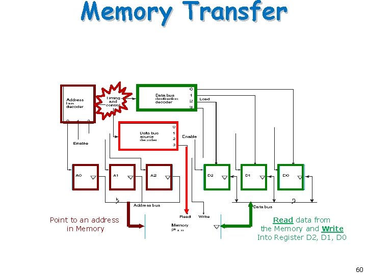
Memory Transfers o Usually one or more buses associated with memory Address q Data q o Note that memory can be slower, so may have to use complex timing Address on one clock cycle q Data latched at later clock cycle q 56

Properties of Memory 1. Volatile o Memory disappears if power goes out • • • 2. Typical computer RAM Static RAM (SRAM), Cache Dynamic RAM (DRAM) Main Memory Nonvolatile o o o ROM Flash memories Magnetic memories like disk, tape 57

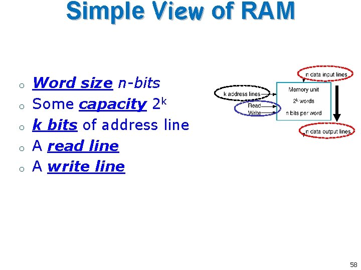
Simple View of RAM o o o Word size n-bits Some capacity 2 k k bits of address line A read line A write line 58
![Memory Transfer o Read DR MAR where o o M denotes Memory Transfer o Read: DR M[AR] where • • • o o M denotes](https://slidetodoc.com/presentation_image/007b97ebeb74cadf1c78bceb2457be9d/image-59.jpg)
Memory Transfer o Read: DR M[AR] where • • • o o M denotes Memory, DR denotes Data Register, Register and AR denotes Address Register Write: M[AR] DR Write: M[A 1] D 2 59

Memory Transfer Point to an address in Memory Read data from the Memory and Write Into Register D 2, D 1, D 0 60

Complete Data Path Design

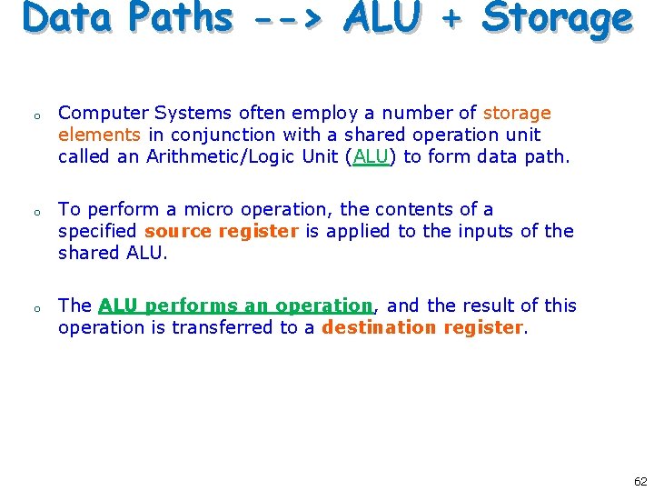
Data Paths --> ALU + Storage o o o Computer Systems often employ a number of storage elements in conjunction with a shared operation unit called an Arithmetic/Logic Unit (ALU) to form data path. To perform a micro operation, the contents of a specified source register is applied to the inputs of the shared ALU. The ALU performs an operation, and the result of this operation is transferred to a destination register. 62

Data Paths, Single Clock Cycle Since the ALU is designed as a pure combinational circuit, the entire register transfer operation from the source registers, through the ALU, and into the destination register is performed in one clock cycle. 63

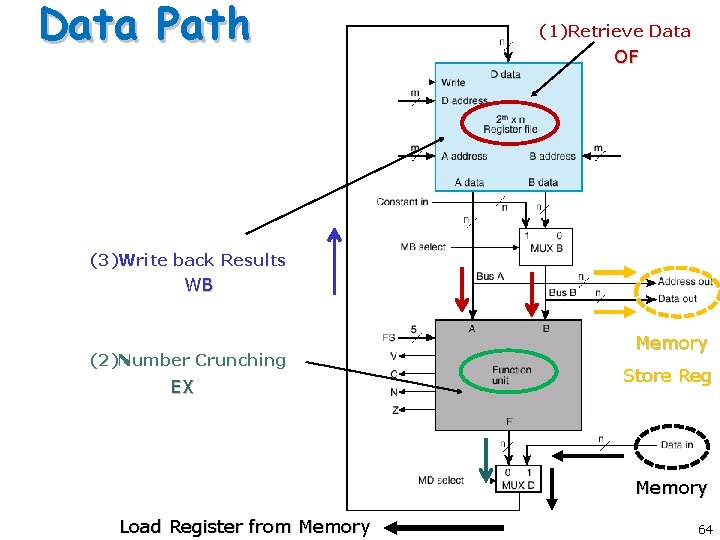
Data Path (1)Retrieve Data OF (3)Write back Results WB (2)Number Crunching EX Memory Store Reg Memory Load Register from Memory 64

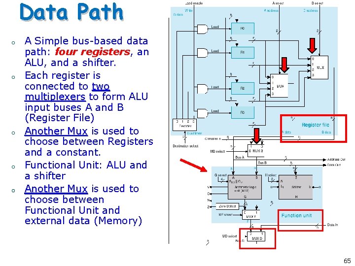
Data Path o o o A Simple bus-based data path: four registers, an ALU, and a shifter. Each register is connected to two multiplexers to form ALU input buses A and B (Register File) Another Mux is used to choose between Registers and a constant. Functional Unit: ALU and a shifter Another Mux is used to choose between Functional Unit and external data (Memory) 65

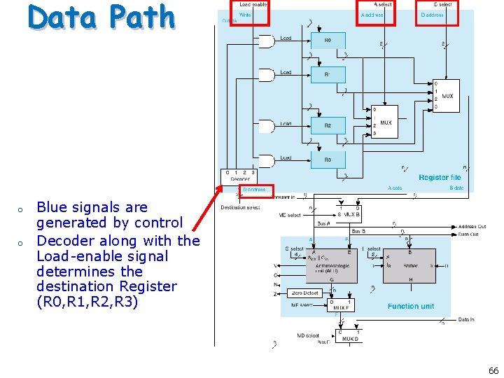
Data Path o o Blue signals are generated by control Decoder along with the Load-enable signal determines the destination Register (R 0, R 1, R 2, R 3) 66

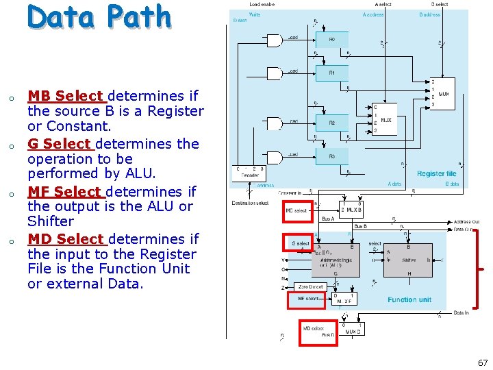
Data Path o o MB Select determines if the source B is a Register or Constant. G Select determines the operation to be performed by ALU. MF Select determines if the output is the ALU or Shifter MD Select determines if the input to the Register File is the Function Unit or external Data. 67

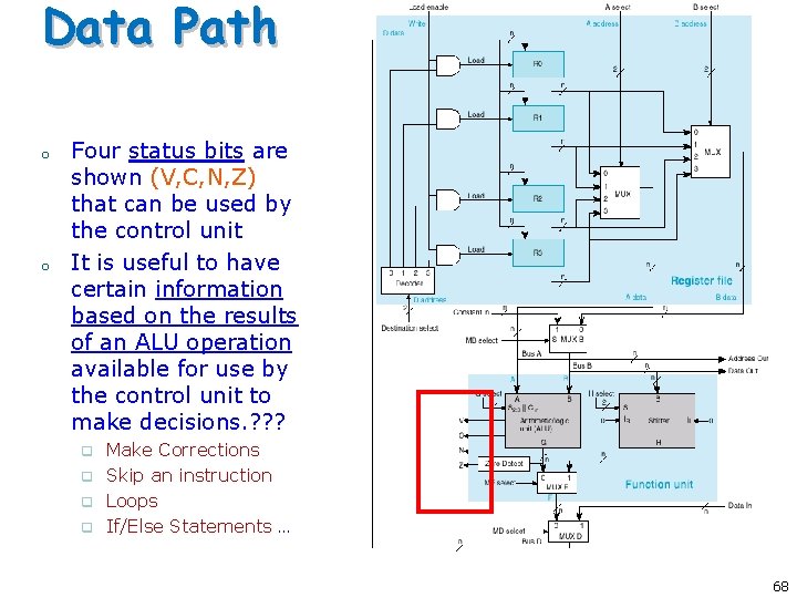
Data Path o o Four status bits are shown (V, C, N, Z) that can be used by the control unit It is useful to have certain information based on the results of an ALU operation available for use by the control unit to make decisions. ? ? ? q q Make Corrections Skip an instruction Loops If/Else Statements … 68

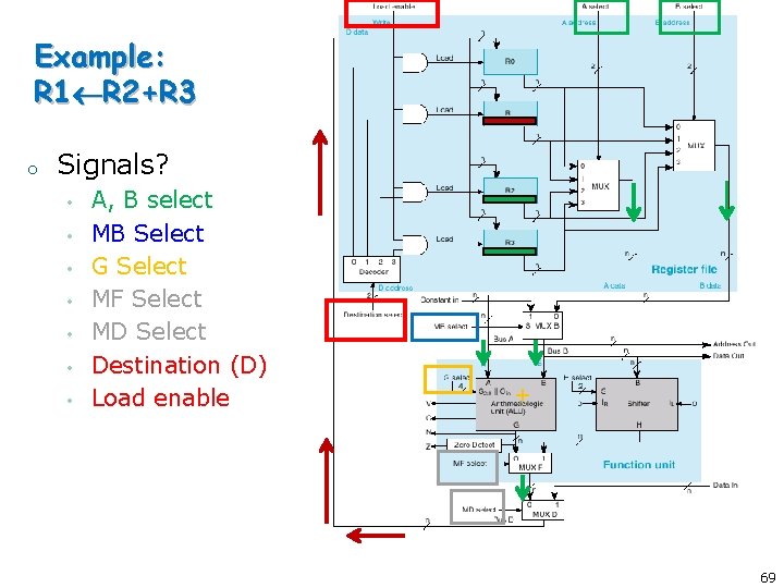
Example: R 1 R 2+R 3 o Signals? • • A, B select MB Select G Select MF Select MD Select Destination (D) Load enable + 69

Timing of Data Path

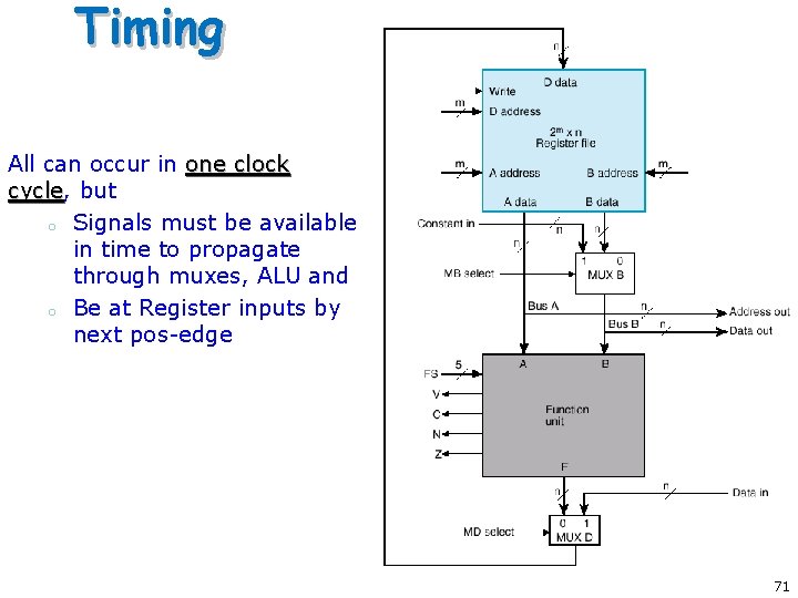
Timing All can occur in one clock cycle, cycle but o Signals must be available in time to propagate through muxes, ALU and o Be at Register inputs by next pos-edge 71

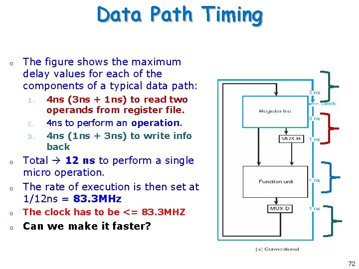
Data Path Timing o The figure shows the maximum delay values for each of the components of a typical data path: 1. 2. 3. o o 4 ns (3 ns + 1 ns) to read two operands from register file. 4 ns to perform an operation. 4 ns (1 ns + 3 ns) to write info back Total 12 ns to perform a single micro operation. The rate of execution is then set at 1/12 ns = 83. 3 MHz o The clock has to be <= 83. 3 MHZ o Can we make it faster? 72

Performance Improvement In addition to providing a data path that performs the necessary register transfer micro operations, we need to be concerned about the speed or rate at which the micro operations are performed. How? I. II. First we need to know the maximum speed by which our data path can be run. Then we will explore how we can make it faster. (Pipelining) 73

Pipelining

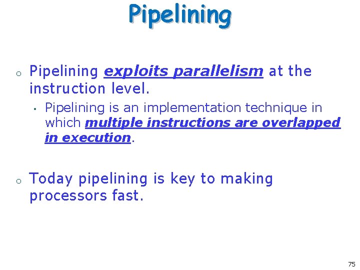
Pipelining o Pipelining exploits parallelism at the instruction level. • o Pipelining is an implementation technique in which multiple instructions are overlapped in execution. Today pipelining is key to making processors fast. 75

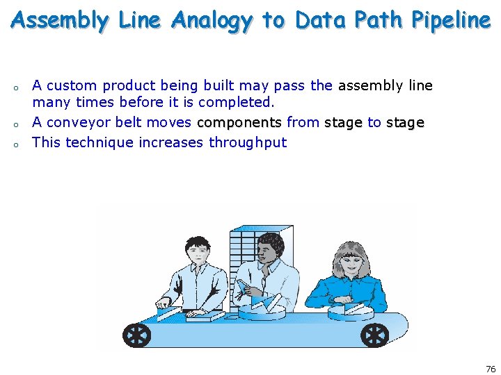
Assembly Line Analogy to Data Path Pipeline o o o A custom product being built may pass the assembly line many times before it is completed. A conveyor belt moves components from stage to stage This technique increases throughput 76

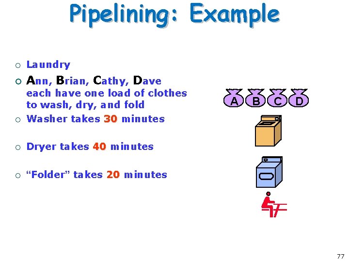
Pipelining: Example ¡ Laundry ¡ Ann, Brian, Cathy, Dave ¡ each have one load of clothes to wash, dry, and fold Washer takes 30 minutes ¡ Dryer takes 40 minutes ¡ “Folder” takes 20 minutes A B C D 77

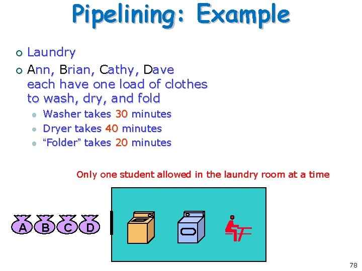
Pipelining: Example Laundry ¡ Ann, Brian, Cathy, Dave each have one load of clothes to wash, dry, and fold ¡ l l l Washer takes 30 minutes Dryer takes 40 minutes “Folder” takes 20 minutes Only one student allowed in the laundry room at a time A B C D 78

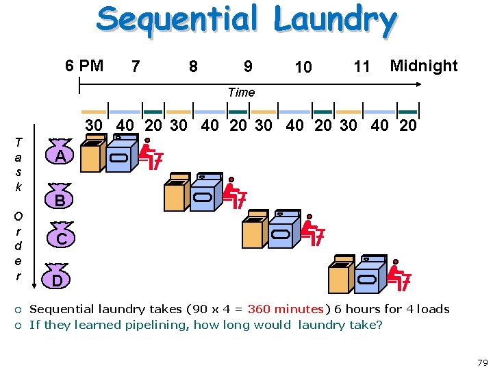
Sequential Laundry 6 PM 7 8 9 10 11 Midnight Time 30 40 20 T a s k O r d e r ¡ ¡ A B C D Sequential laundry takes (90 x 4 = 360 minutes) 6 hours for 4 loads If they learned pipelining, how long would laundry take? 79

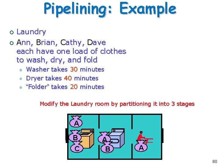
Pipelining: Example Laundry ¡ Ann, Brian, Cathy, Dave each have one load of clothes to wash, dry, and fold ¡ l l l Washer takes 30 minutes Dryer takes 40 minutes “Folder” takes 20 minutes Modify the Laundry room by partitioning it into 3 stages A B C A B A 80

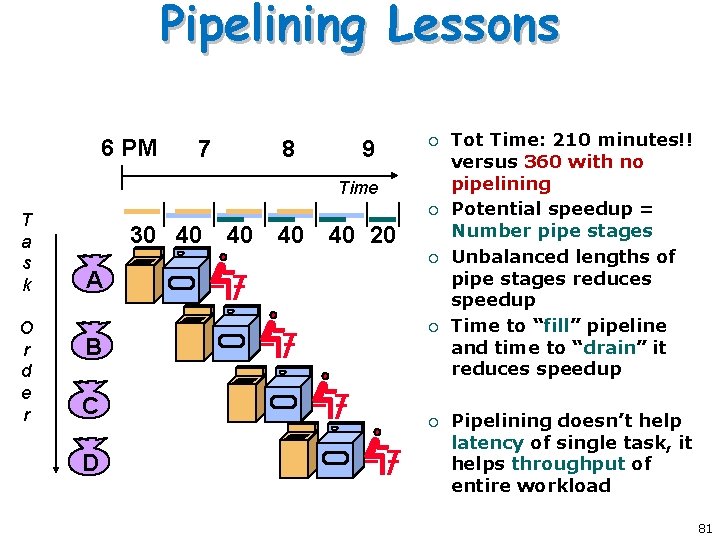
Pipelining Lessons 6 PM 7 8 9 ¡ Time T a s k O r d e r ¡ 30 40 40 20 ¡ A B C D ¡ ¡ Tot Time: 210 minutes!! versus 360 with no pipelining Potential speedup = Number pipe stages Unbalanced lengths of pipe stages reduces speedup Time to “fill” pipeline and time to “drain” it reduces speedup Pipelining doesn’t help latency of single task, it helps throughput of entire workload 81

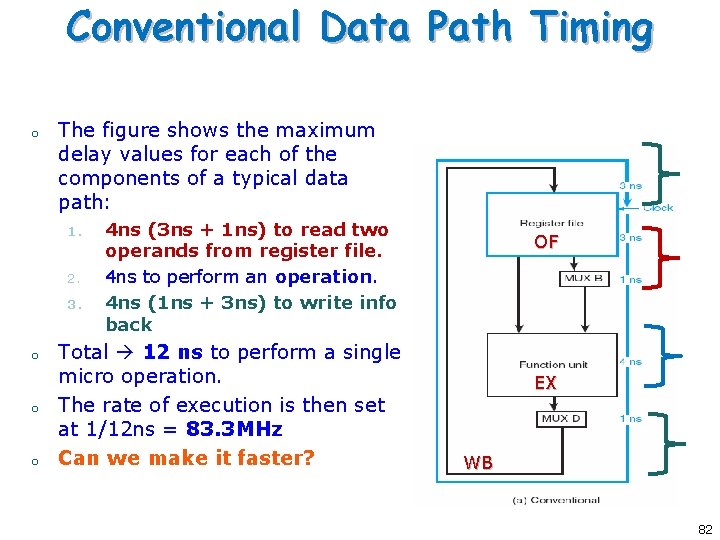
Conventional Data Path Timing o The figure shows the maximum delay values for each of the components of a typical data path: 1. 2. 3. o o o 4 ns (3 ns + 1 ns) to read two operands from register file. 4 ns to perform an operation. 4 ns (1 ns + 3 ns) to write info back Total 12 ns to perform a single micro operation. The rate of execution is then set at 1/12 ns = 83. 3 MHz Can we make it faster? OF EX WB 82

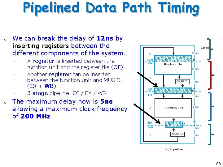
Pipelined Data Path Timing o We can break the delay of 12 ns by inserting registers between the different components of the system. • • • o A register is inserted between the function unit and the register file (OF) Another register can be inserted between the function unit and MUX D. (EX + WB) 3 stage pipeline: OF / EX / WB The maximum delay now is 5 ns allowing a maximum clock frequency of 200 MHz 83

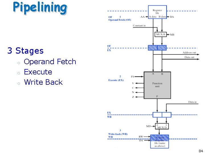
Pipelining 3 Stages o o o Operand Fetch Execute Write Back 84 84

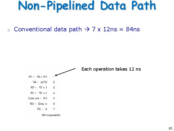
Non-Pipelined Data Path o Conventional data path 7 x 12 ns = 84 ns Each operation takes 12 ns 85

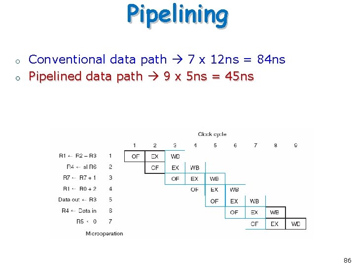
Pipelining o o Conventional data path 7 x 12 ns = 84 ns Pipelined data path 9 x 5 ns = 45 ns 86

Summary o o Data Paths are an essential part of any CPU. ALUs (Arithmetic Logic Units) are at the heart of any Data Path. Multiplexors and Tri-State buffers are used extensively in Data Paths (data movement) Pipelining is a technique to: o o Improve throughput by overlapping instruction execution. Does not improve the latency of each instruction. . 87
