EMT 362 Microelectronic Fabrication CMOS WELL TECHNOLOGY Part
EMT 362: Microelectronic Fabrication CMOS WELL TECHNOLOGY Part 2 Ramzan Mat Ayub School of Microelectronic Engineering
• In CMOS Technology, both n and p-channel transistor must be fabricated on the same wafer. • To accommodate the device type that cannot be built on the particular substrate, regions of a doping type opposite to the substrate must be formed. • These regions are called WELL and normally the first module to be introduced. • Excess dopants are selectively introduced to achieve a certain depth and concentration profile. School of Microelectronic Engineering
TYPE OF WELLS • P Well • N-Well • Twin-Well On P OR N-type Substrate • Retrograde Well School of Microelectronic Engineering
P – WELL CMOS • The p-well process, involves the creation of p-regions in n-type substrate for the fabrication of n-channel transistor. • The p-wells are formed by implanting a p-type dopant into an n-substrate. • The n-substrate doping level normally between 3 x 10¹⁴ to 1 x 10¹⁵, and p-well doping concentration normally done at 5 to 10 times higher. School of Microelectronic Engineering
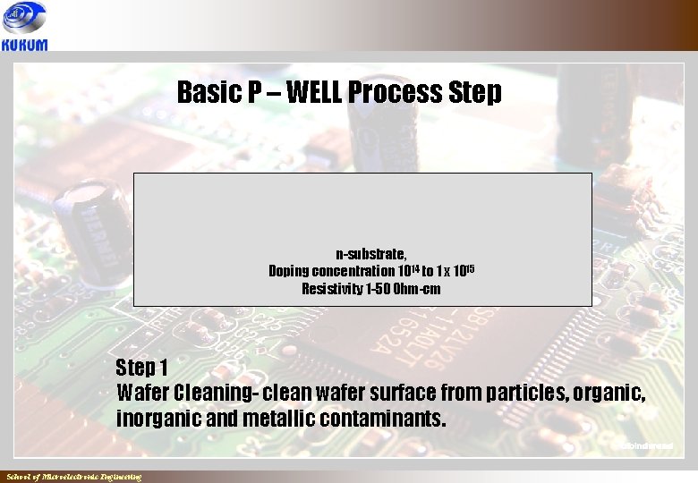
Basic P – WELL Process Step n-substrate, Doping concentration 1014 to 1 x 10¹⁵ Resistivity 1 -50 Ohm-cm Step 1 Wafer Cleaning- clean wafer surface from particles, organic, inorganic and metallic contaminants. School of Microelectronic Engineering
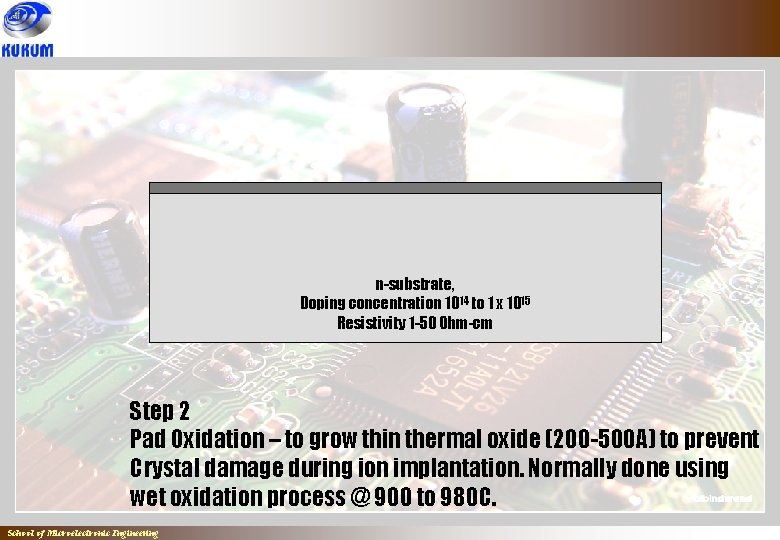
n-substrate, Doping concentration 1014 to 1 x 10¹⁵ Resistivity 1 -50 Ohm-cm Step 2 Pad Oxidation – to grow thin thermal oxide (200 -500 A) to prevent Crystal damage during ion implantation. Normally done using wet oxidation process @ 900 to 980 C. School of Microelectronic Engineering
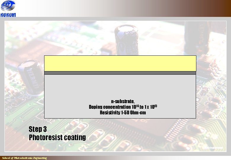
n-substrate, Doping concentration 1014 to 1 x 10¹⁵ Resistivity 1 -50 Ohm-cm Step 3 Photoresist coating School of Microelectronic Engineering
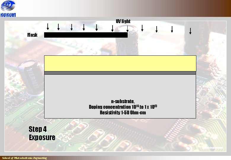
UV light Mask n-substrate, Doping concentration 1014 to 1 x 10¹⁵ Resistivity 1 -50 Ohm-cm Step 4 Exposure School of Microelectronic Engineering
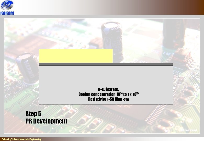
n-substrate, Doping concentration 1014 to 1 x 10¹⁵ Resistivity 1 -50 Ohm-cm Step 5 PR Development School of Microelectronic Engineering
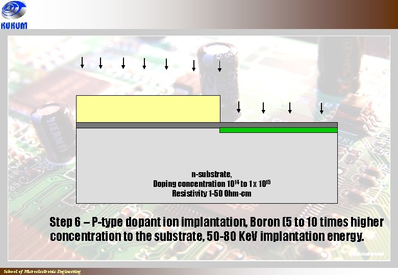
n-substrate, Doping concentration 1014 to 1 x 10¹⁵ Resistivity 1 -50 Ohm-cm Step 6 – P-type dopant ion implantation, Boron (5 to 10 times higher concentration to the substrate, 50 -80 Ke. V implantation energy. School of Microelectronic Engineering
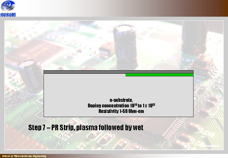
n-substrate, Doping concentration 1014 to 1 x 10¹⁵ Resistivity 1 -50 Ohm-cm Step 7 – PR Strip, plasma followed by wet School of Microelectronic Engineering
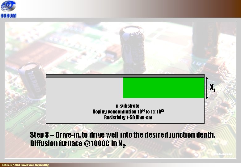
Xj n-substrate, Doping concentration 1014 to 1 x 10¹⁵ Resistivity 1 -50 Ohm-cm Step 8 – Drive-in, to drive well into the desired junction depth. Diffusion furnace @ 1000 C in N 2. School of Microelectronic Engineering
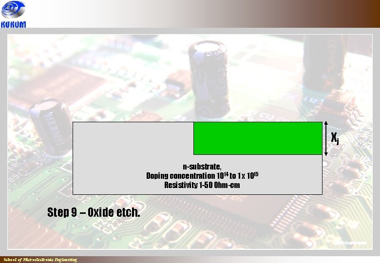
Xj n-substrate, Doping concentration 1014 to 1 x 10¹⁵ Resistivity 1 -50 Ohm-cm Step 9 – Oxide etch. School of Microelectronic Engineering
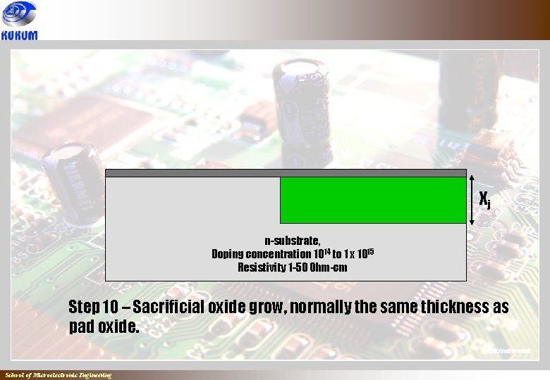
Xj n-substrate, Doping concentration 1014 to 1 x 10¹⁵ Resistivity 1 -50 Ohm-cm Step 10 – Sacrificial oxide grow, normally the same thickness as pad oxide. School of Microelectronic Engineering
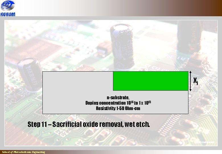
Xj n-substrate, Doping concentration 1014 to 1 x 10¹⁵ Resistivity 1 -50 Ohm-cm Step 11 – Sacrificial oxide removal, wet etch. School of Microelectronic Engineering
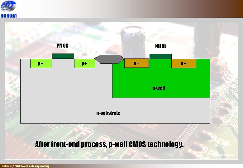
PMOS p+ NMOS n+ p+ n+ p-well n-substrate After front-end process, p-well CMOS technology. School of Microelectronic Engineering
• The 1 st CMOS technology, commercially introduced in early 60 s. • Advantages over n-well CMOS • balanced performance for both NMOS and PMOS (good for pure logic product) • suit better for application required isolated p-region (n-channel FET for analog) • less susceptible to field inversion problem (p-well can be used as a channel stop) • better for SRAM product (soft error rate factor) • Disadvantages over n-well CMOS • NMOS performance degradation • harder to handle substrate current from well, since NMOS produce more hot carriers School of Microelectronic Engineering
N – WELL CMOS • The n-well process, involves the creation of n-regions in p-type substrate for the fabrication of p-channel transistor. • The n-wells are formed by implanting a n-type dopant into an n-substrate. • The p-substrate doping level normally between 3 x 10¹⁴ to 1 x 10¹⁵, and n-well doping concentration normally done at 5 to 10 times higher. School of Microelectronic Engineering
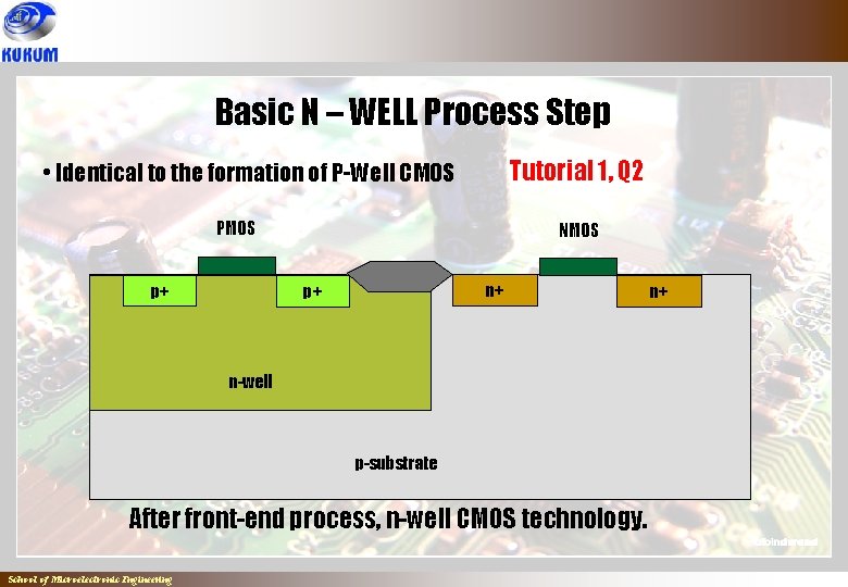
Basic N – WELL Process Step Tutorial 1, Q 2 • Identical to the formation of P-Well CMOS PMOS p+ NMOS n+ p+ n-well p-substrate After front-end process, n-well CMOS technology. School of Microelectronic Engineering n+
• Advantages over p-well CMOS • Performs better in high speed, high density applications (majority of EPROM, DRAM and Micro. P in 1. 25 to 2 um process technology were implemented using n-well CMOS). • Disadvantages over p-well CMOS • Sensitive to field inversion, need an additional channel stop process School of Microelectronic Engineering
Example An n-well CMOS process is to be developed for operation with power supply voltage of VDD=5 V. The substrate doping of the p-type wafer is 1 x 10¹⁵ atoms / cm 3. The n-wells are to have an average doping concentration of 1 x 10 16 atoms/cm 3. The p-channel MOSFET sources and drains are to have junction depths of 0. 4 um and average dopant density of 1 x 10¹⁸ atoms/cm 3. What is the minimum N-well depth needed to avoid vertical puncthrough to the substrate? School of Microelectronic Engineering
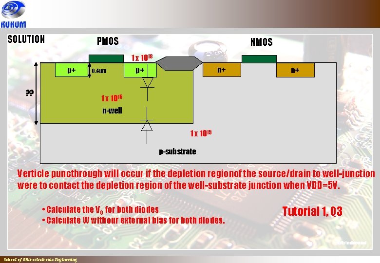
SOLUTION PMOS NMOS 1 x 10¹⁸ p+ ? ? 0. 4 um n+ p+ n+ 1 x 10¹⁶ n-well 1 x 10¹⁵ p-substrate Verticle puncthrough will occur if the depletion regionof the source/drain to well-junction were to contact the depletion region of the well-substrate junction when VDD=5 V. • Calculate the V 0 for both diodes • Calculate W withour external bias for both diodes. School of Microelectronic Engineering Tutorial 1, Q 3
TWIN–WELL CMOS • Two separate wells are formed for n and p-channel transistors on a lightly doped substrate. • The substrate maybe either a lightly doped n or p-type material, or a thin, lightly doped epitaxial layer. • Each of the wells dopants is implanted separately and then driven to the desired depth. School of Microelectronic Engineering
Basic TWIN – WELL Process Step n or p or epi-substrate, Step 1 Wafer Cleaning- clean wafer surface from particles, organic, inorganic and metallic contaminants. School of Microelectronic Engineering

Step 2 Pad Oxidation – to grow thin thermal oxide (200 -500 A) to prevent Crystal damage during ion implantation. Normally done using wet oxidation process @ 900 to 980 C. School of Microelectronic Engineering

Step 3 Silicon nitride deposition – masking for p-channel area. Normally done using LPCVD or PECVD process. Typical thickness between 1500 – 2000 A. School of Microelectronic Engineering
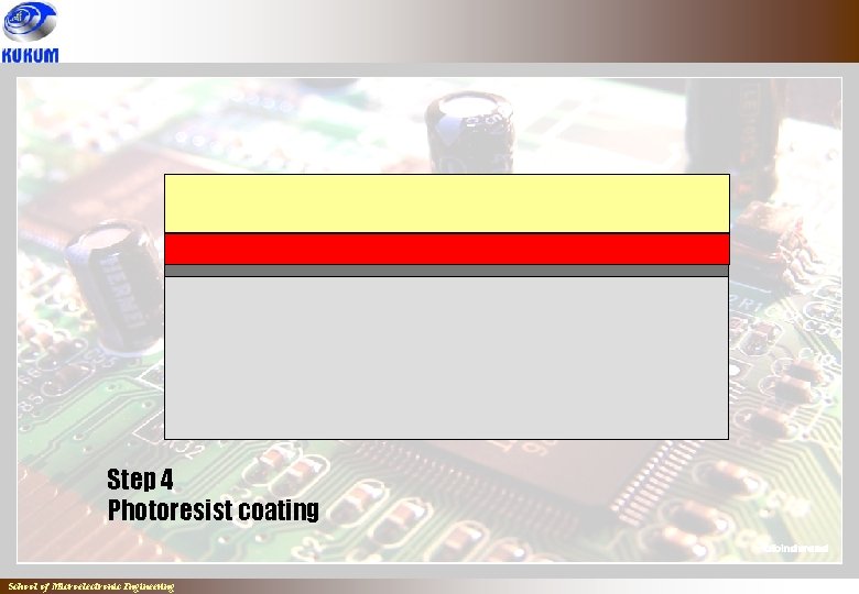
Step 4 Photoresist coating School of Microelectronic Engineering
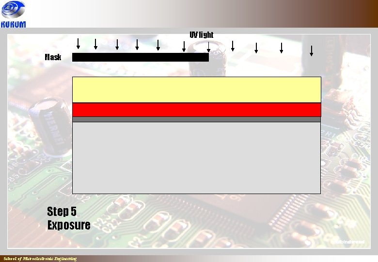
UV light Mask Step 5 Exposure School of Microelectronic Engineering
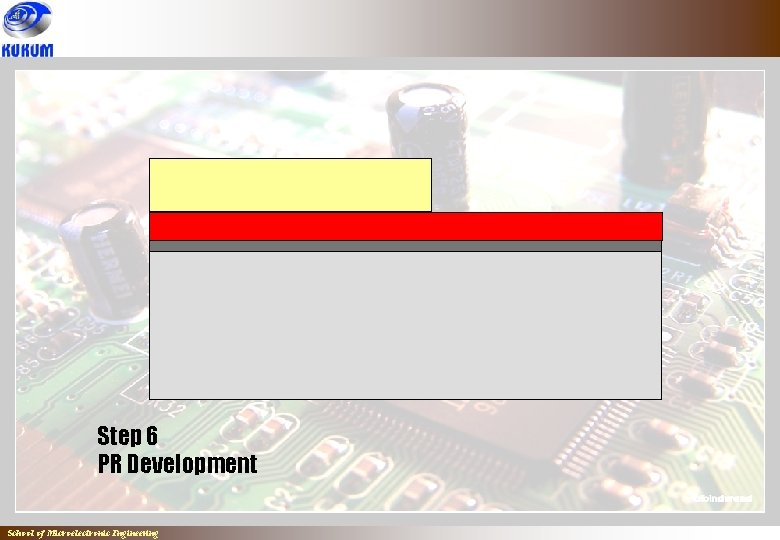
Step 6 PR Development School of Microelectronic Engineering
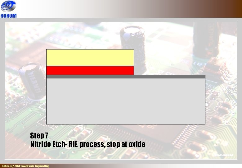
Step 7 Nitride Etch- RIE process, stop at oxide School of Microelectronic Engineering
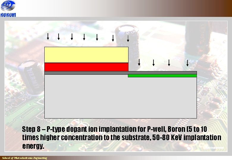
Step 8 – P-type dopant ion implantation for P-well, Boron (5 to 10 times higher concentration to the substrate, 50 -80 Ke. V implantation energy. School of Microelectronic Engineering
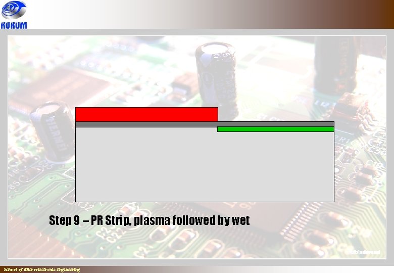
Step 9 – PR Strip, plasma followed by wet School of Microelectronic Engineering
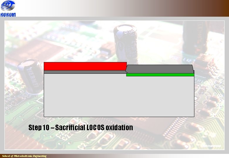
Step 10 – Sacrificial LOCOS oxidation School of Microelectronic Engineering
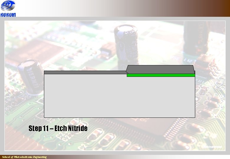
Step 11 – Etch Nitride School of Microelectronic Engineering
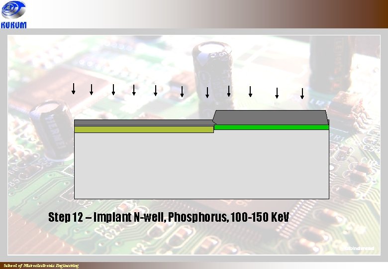
Step 12 – Implant N-well, Phosphorus, 100 -150 Ke. V School of Microelectronic Engineering
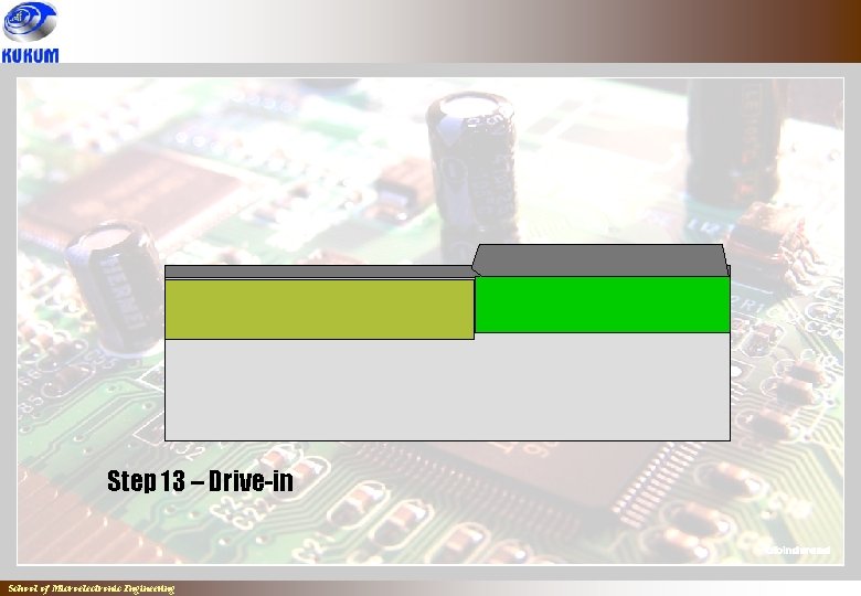
Step 13 – Drive-in School of Microelectronic Engineering
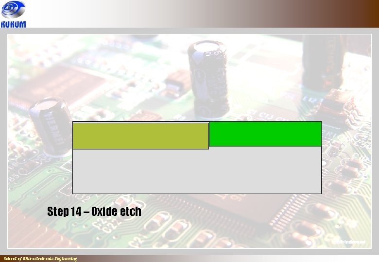
Step 14 – Oxide etch School of Microelectronic Engineering
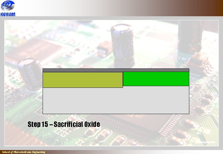
Step 15 – Sacrificial Oxide School of Microelectronic Engineering
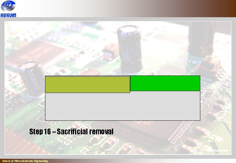
Step 16 – Sacrificial removal School of Microelectronic Engineering
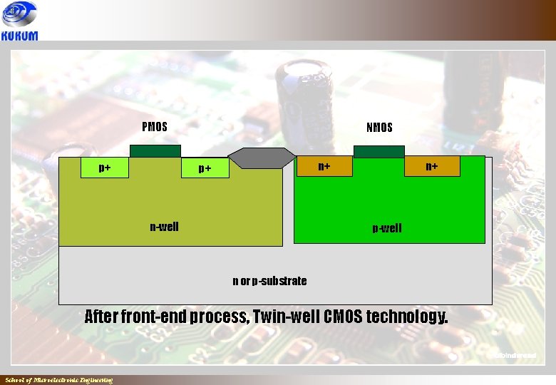
PMOS p+ NMOS n+ n+ p+ n-well p-well n or p-substrate After front-end process, Twin-well CMOS technology. School of Microelectronic Engineering
• The most widely used well scheme in sub-micron CMOS technology • Advantages • Doping profile for each device can be set independently. • Compatibility with advanced isolation structure (trench and SEG), allow closer n+ to p+ spacing design rules i. e denser circuit. • substrate can be changed without changing the process flow • enable the implementation of self aligned channel stop. School of Microelectronic Engineering
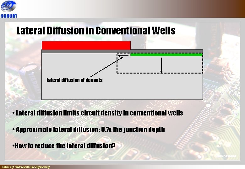
Lateral Diffusion in Conventional Wells Lateral diffusion of dopants • Lateral diffusion limits circuit density in conventional wells • Approximate lateral diffusion; 0. 7 x the junction depth • How to reduce the lateral diffusion? School of Microelectronic Engineering
Retrograde Well • Use high energy implant, followed by short annealing step. Well formed by this technique is called Retrograde Well • Temperature cycle of subsequent process is tightly controlled. School of Microelectronic Engineering
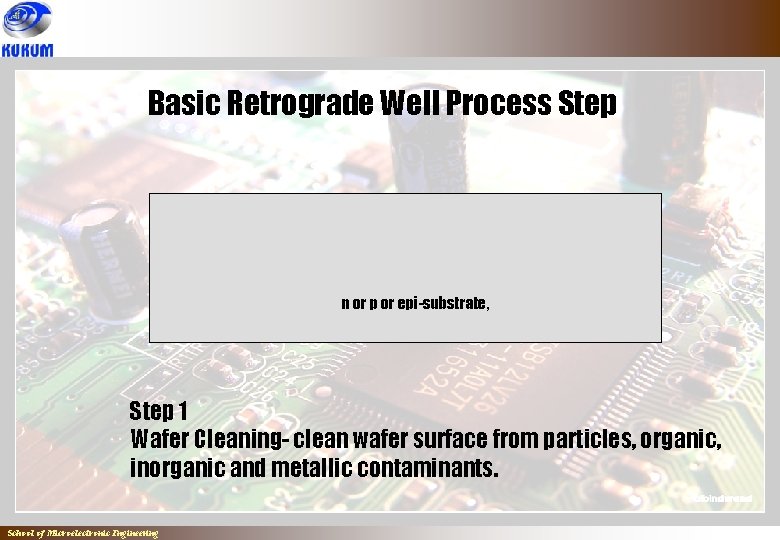
Basic Retrograde Well Process Step n or p or epi-substrate, Step 1 Wafer Cleaning- clean wafer surface from particles, organic, inorganic and metallic contaminants. School of Microelectronic Engineering
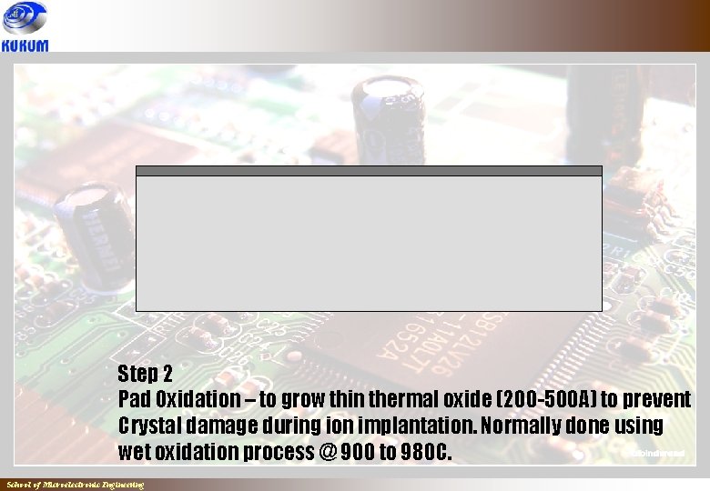
Step 2 Pad Oxidation – to grow thin thermal oxide (200 -500 A) to prevent Crystal damage during ion implantation. Normally done using wet oxidation process @ 900 to 980 C. School of Microelectronic Engineering
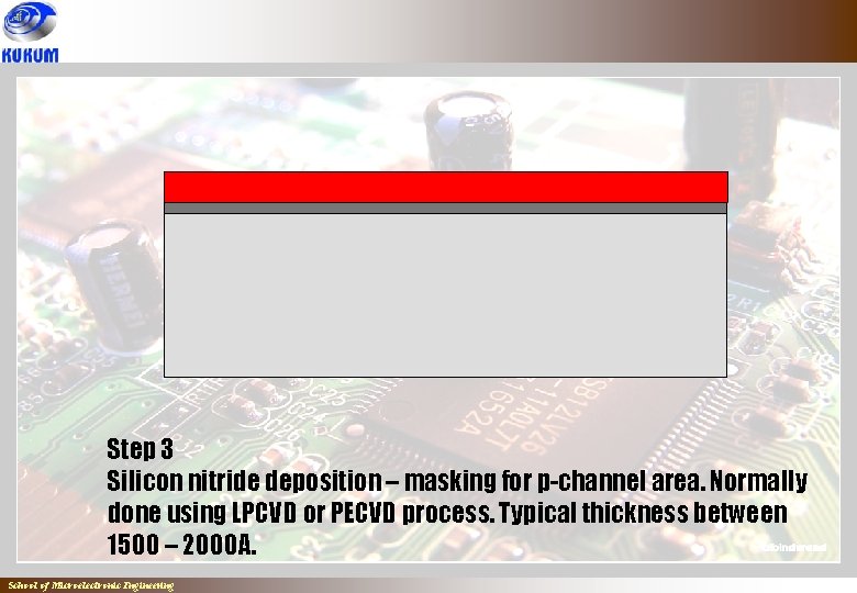
Step 3 Silicon nitride deposition – masking for p-channel area. Normally done using LPCVD or PECVD process. Typical thickness between 1500 – 2000 A. School of Microelectronic Engineering
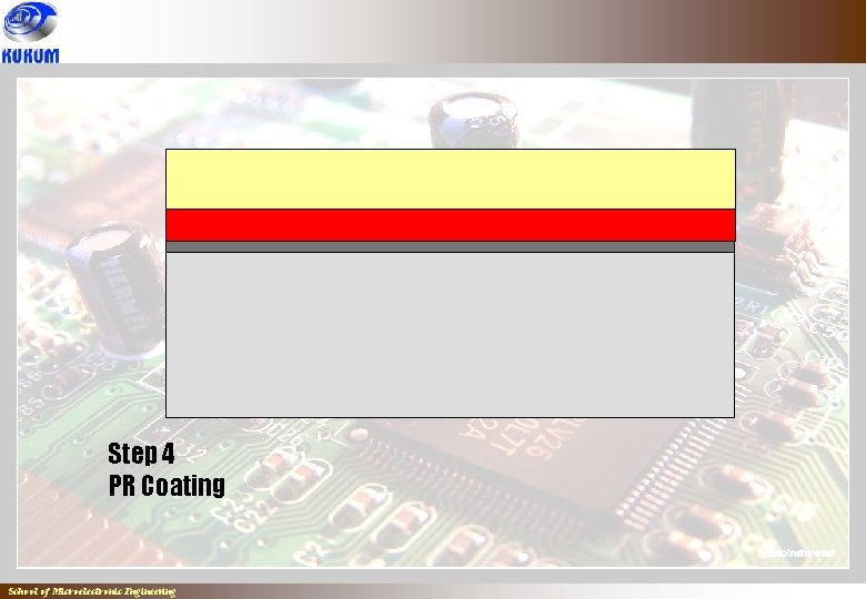
Step 4 PR Coating School of Microelectronic Engineering
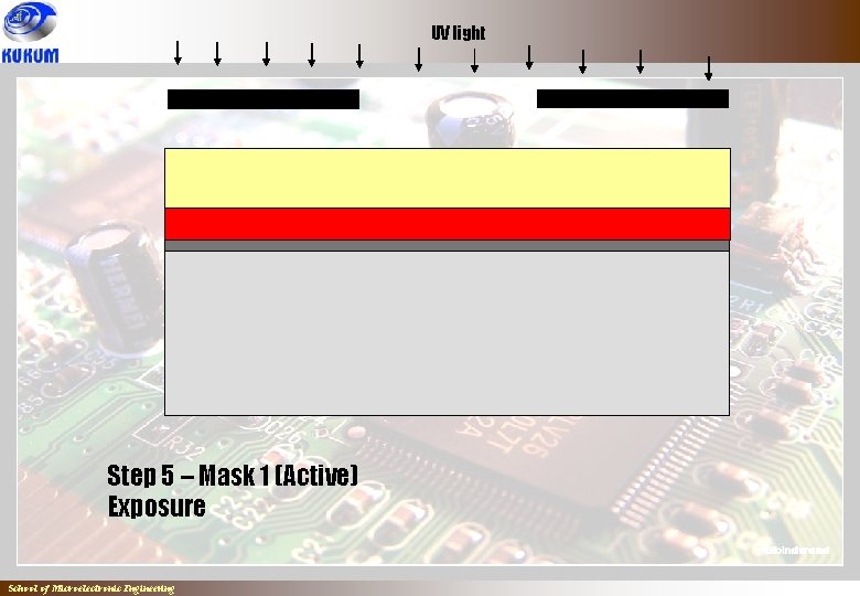
UV light Step 5 – Mask 1 (Active) Exposure School of Microelectronic Engineering
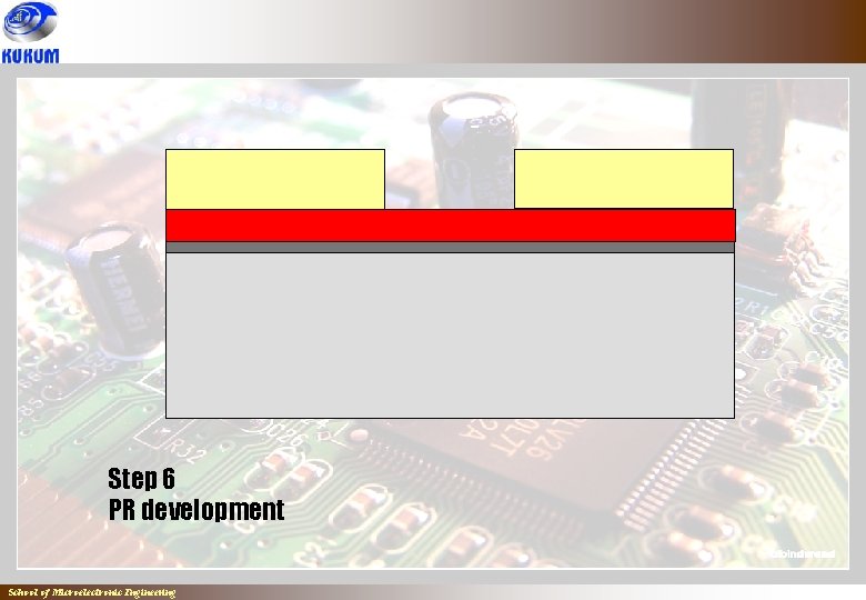
Step 6 PR development School of Microelectronic Engineering
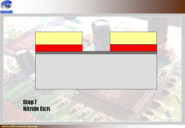
Step 7 Nitride Etch School of Microelectronic Engineering
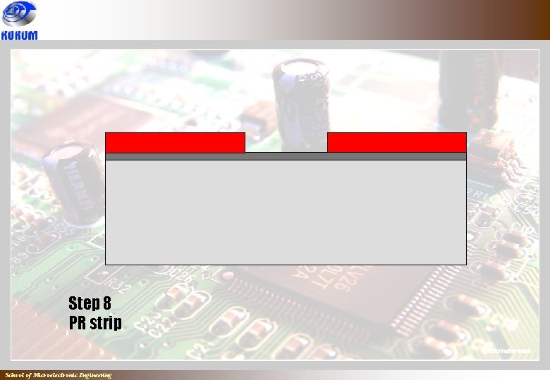
Step 8 PR strip School of Microelectronic Engineering
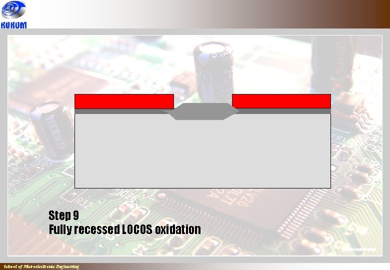
Step 9 Fully recessed LOCOS oxidation School of Microelectronic Engineering
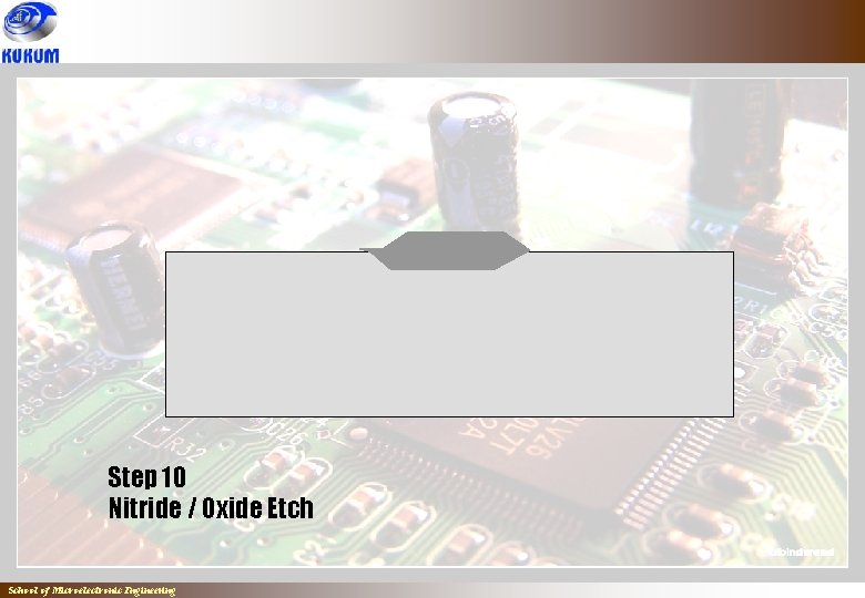
Step 10 Nitride / Oxide Etch School of Microelectronic Engineering
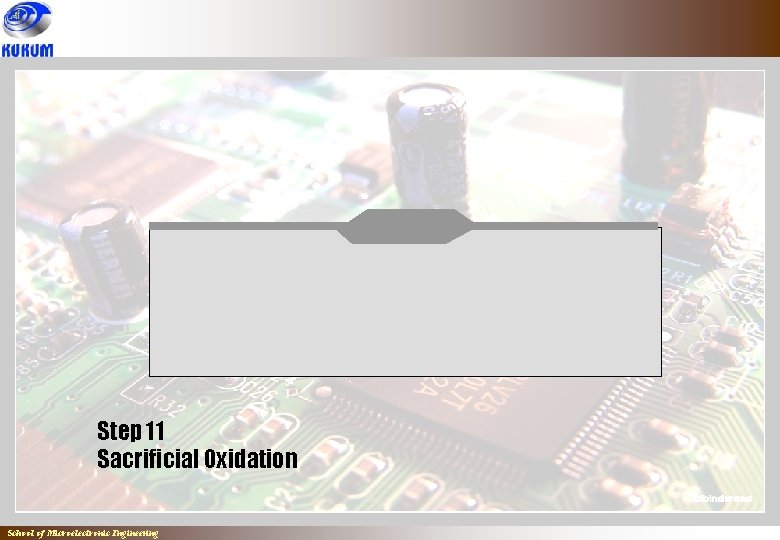
Step 11 Sacrificial Oxidation School of Microelectronic Engineering
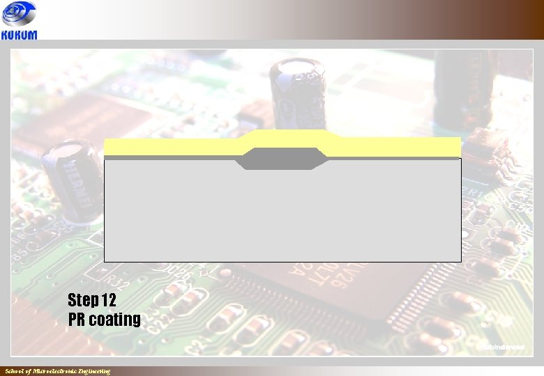
Step 12 PR coating School of Microelectronic Engineering
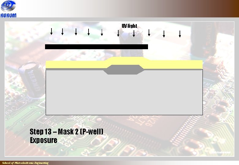
UV light Step 13 – Mask 2 (P-well) Exposure School of Microelectronic Engineering
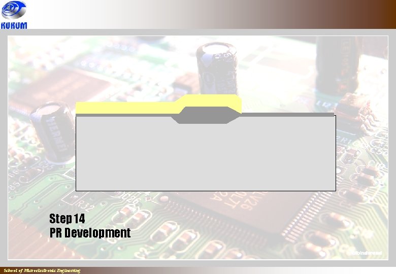
Step 14 PR Development School of Microelectronic Engineering
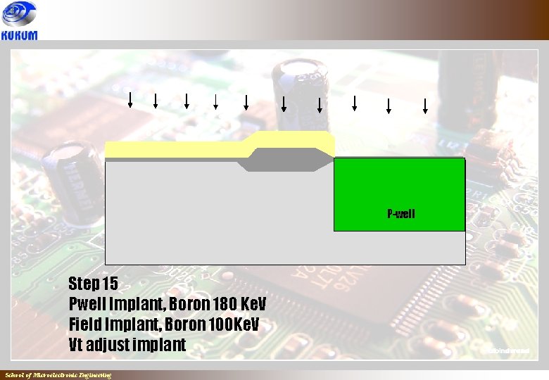
P-well Step 15 Pwell Implant, Boron 180 Ke. V Field Implant, Boron 100 Ke. V Vt adjust implant School of Microelectronic Engineering
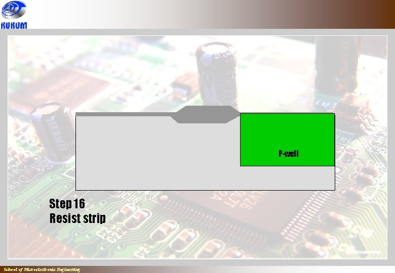
P-well Step 16 Resist strip School of Microelectronic Engineering
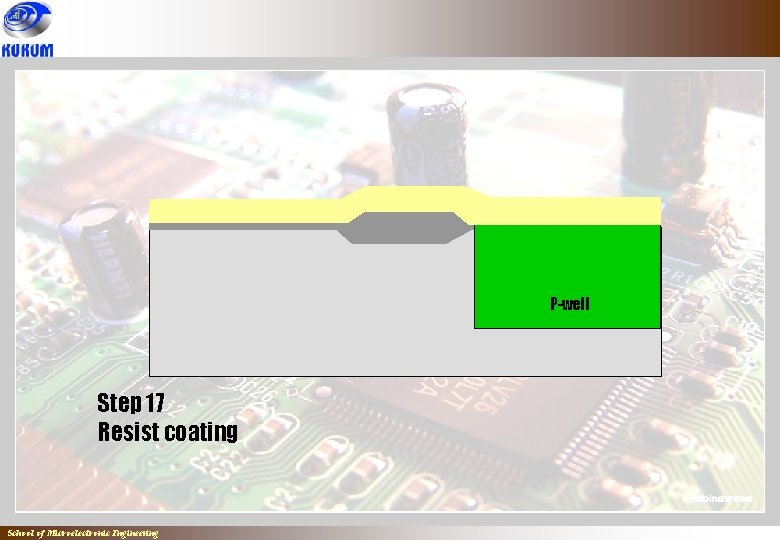
P-well Step 17 Resist coating School of Microelectronic Engineering
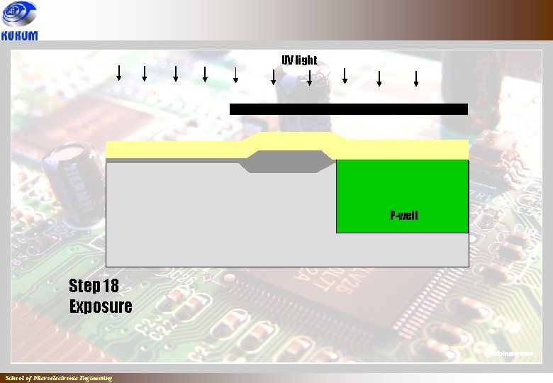
UV light P-well Step 18 Exposure School of Microelectronic Engineering
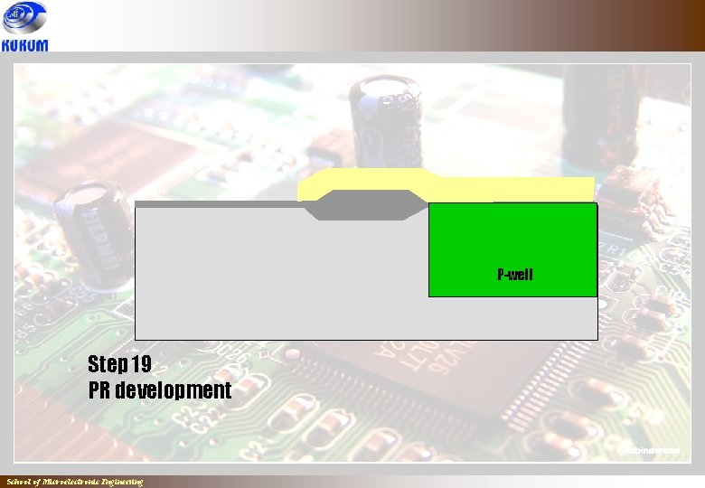
P-well Step 19 PR development School of Microelectronic Engineering
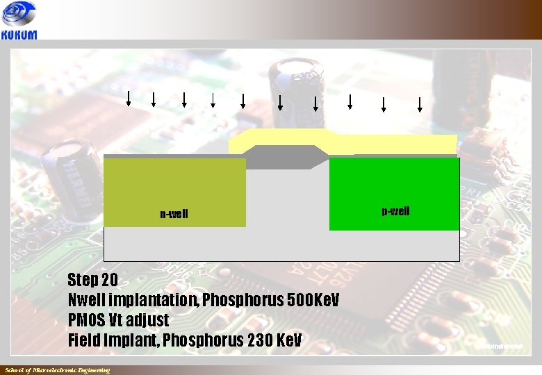
n-well Step 20 Nwell implantation, Phosphorus 500 Ke. V PMOS Vt adjust Field Implant, Phosphorus 230 Ke. V School of Microelectronic Engineering p-well
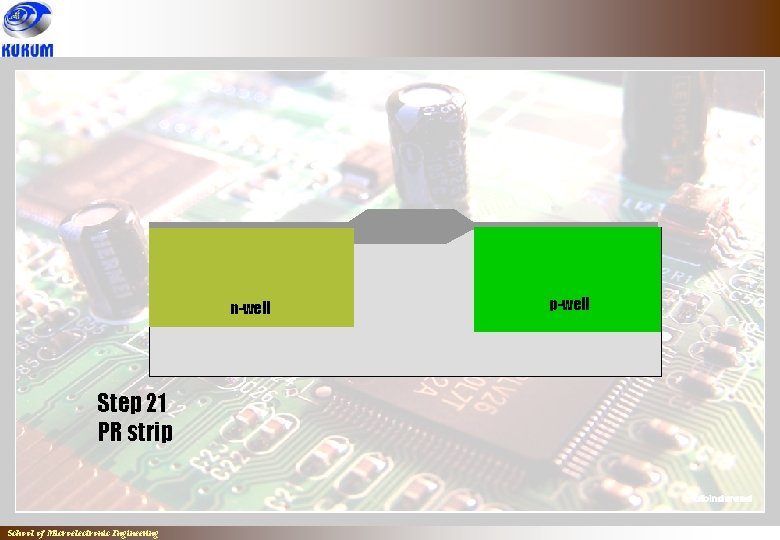
n-well Step 21 PR strip School of Microelectronic Engineering p-well
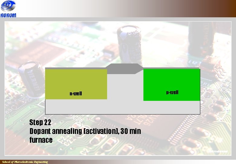
n-well Step 22 Dopant annealing (activation), 30 min furnace School of Microelectronic Engineering p-well
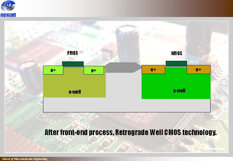
PMOS p+ NMOS p+ n-well n+ n+ p-well After front-end process, Retrograde Well CMOS technology. School of Microelectronic Engineering
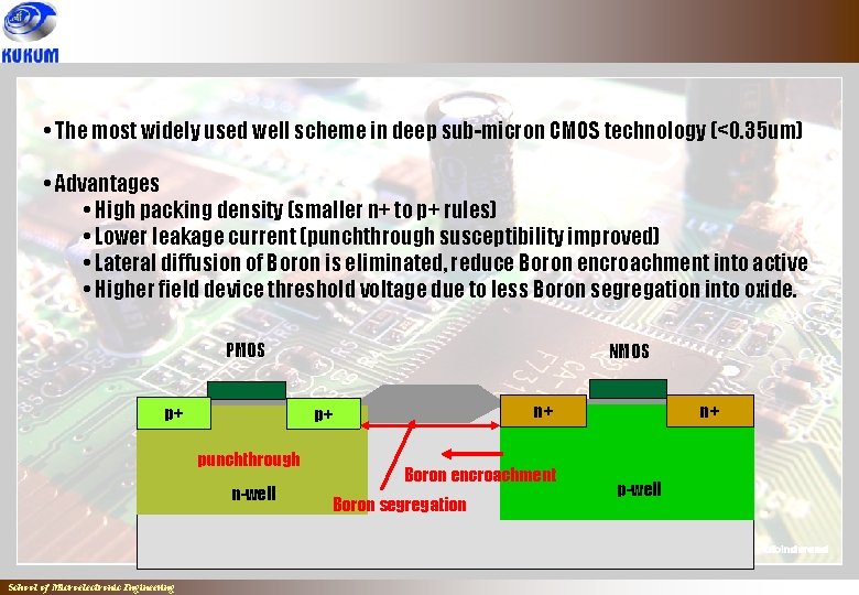
• The most widely used well scheme in deep sub-micron CMOS technology (<0. 35 um) • Advantages • High packing density (smaller n+ to p+ rules) • Lower leakage current (punchthrough susceptibility improved) • Lateral diffusion of Boron is eliminated, reduce Boron encroachment into active • Higher field device threshold voltage due to less Boron segregation into oxide. PMOS p+ n-well n+ n+ p+ punchthrough School of Microelectronic Engineering NMOS Boron encroachment Boron segregation p-well
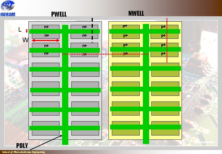
NWELL PWELL L W n+ n+ p+ p+ POLY School of Microelectronic Engineering
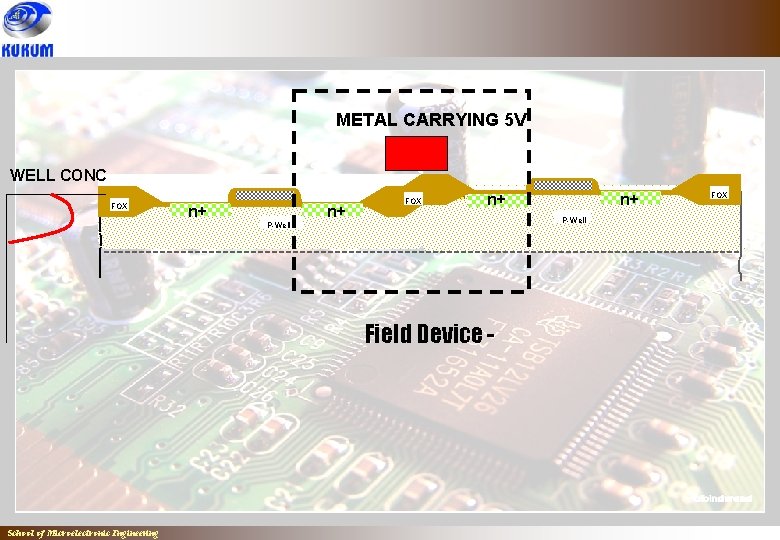
METAL CARRYING 5 V WELL CONC FOX n+ n+ FOX P-Well Field Device - School of Microelectronic Engineering n+ n+ FOX
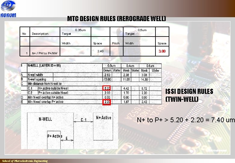
MTC DESIGN RULES (REROGRADE WELL) No Description 0. 35 um Target 0. 5 um Target Width Space Pitch Width Space 1 N+ / PW to P+/NW 2. 40 3. 00 ISSI DESIGN RULES (TWIN-WELL) N+ to P+ > 5. 20 + 2. 20 = 7. 40 um School of Microelectronic Engineering
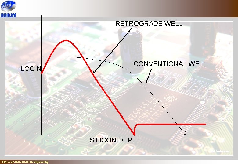
RETROGRADE WELL LOG N CONVENTIONAL WELL SILICON DEPTH School of Microelectronic Engineering
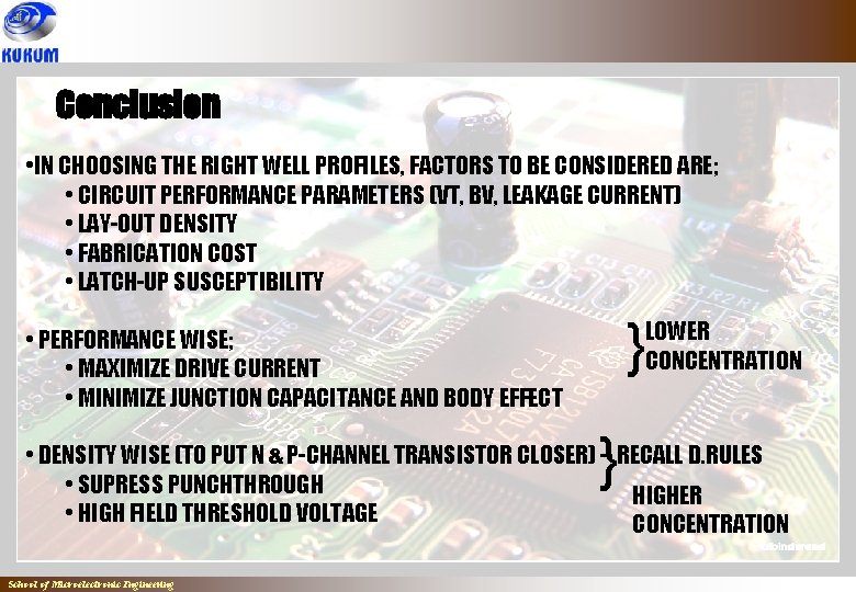
Conclusion • IN CHOOSING THE RIGHT WELL PROFILES, FACTORS TO BE CONSIDERED ARE; • CIRCUIT PERFORMANCE PARAMETERS (VT, BV, LEAKAGE CURRENT) • LAY-OUT DENSITY • FABRICATION COST • LATCH-UP SUSCEPTIBILITY } • PERFORMANCE WISE; • MAXIMIZE DRIVE CURRENT • MINIMIZE JUNCTION CAPACITANCE AND BODY EFFECT } LOWER CONCENTRATION • DENSITY WISE (TO PUT N & P-CHANNEL TRANSISTOR CLOSER) – RECALL D. RULES • SUPRESS PUNCHTHROUGH HIGHER • HIGH FIELD THRESHOLD VOLTAGE CONCENTRATION School of Microelectronic Engineering
- Slides: 72