EMT 182 ANALOG ELECTRONICS I Introduction to Metal
- Slides: 18

EMT 182 ANALOG ELECTRONICS I Introduction to Metal Oxide Semiconductor Field Effect Transistor (MOSFET)

FET Advantages • Voltage-controlled amplifier: input impedance very high • Low noise output: useful as preamplifiers when noise must be very low because of high gain in following stages • Better linearity: distortion minimized • Low inter-electrode capacity: at high frequency, interelectrode capacitance can make amplifier work poorly. FET desirable in RF stages

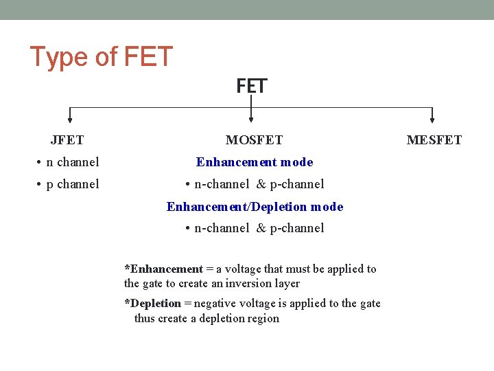
Type of FET JFET MOSFET • n channel Enhancement mode • p channel • n-channel & p-channel Enhancement/Depletion mode • n-channel & p-channel *Enhancement = a voltage that must be applied to the gate to create an inversion layer *Depletion = negative voltage is applied to the gate thus create a depletion region MESFET

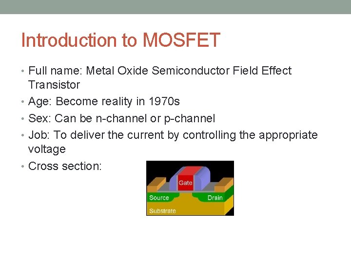
Introduction to MOSFET • Full name: Metal Oxide Semiconductor Field Effect Transistor • Age: Become reality in 1970 s • Sex: Can be n-channel or p-channel • Job: To deliver the current by controlling the appropriate voltage • Cross section:

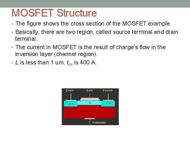
MOSFET Structure • The figure shows the cross section of the MOSFET example. • Basically, there are two region, called source terminal and drain terminal. • The current in MOSFET is the result of charge’s flow in the inversion layer (channel region). • L is less than 1 um. tox is 400 A.

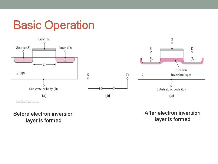
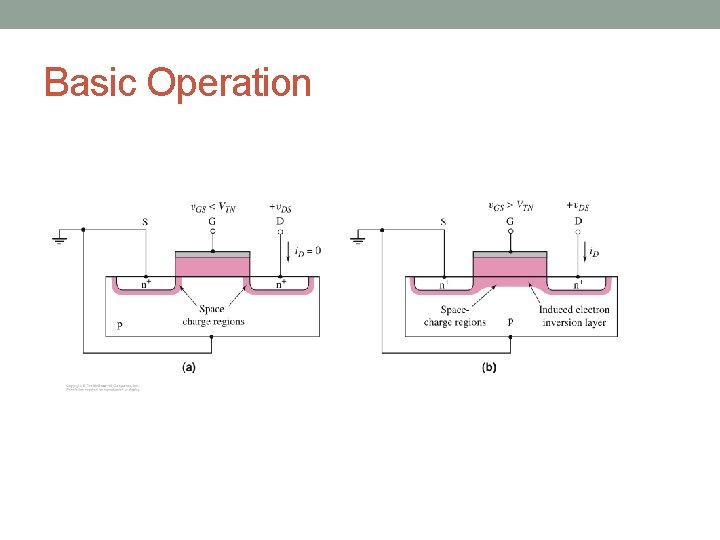
NMOS Basic • With zero bias applied to the gate, source-drain terminals are separated by p-region. Current = 0 A. • If large enough +gate voltage applied, an electron inversion layer is created at oxide-semiconductor interface. • This layer ‘connect’ the n-source and n-drain. • Since the carriers in inversion layer are electrons, this device called n-channel MOSFET (NMOS). • Since voltage must be applied to the gate to create inversion layer, it is called enhancement-mode MOSFET. • Source terminal supplies carriers that flow through channel. • Drain terminal allows carriers to drain from the channel • Electron flow from source-to-drain, and current enter the drain and leaves the source.

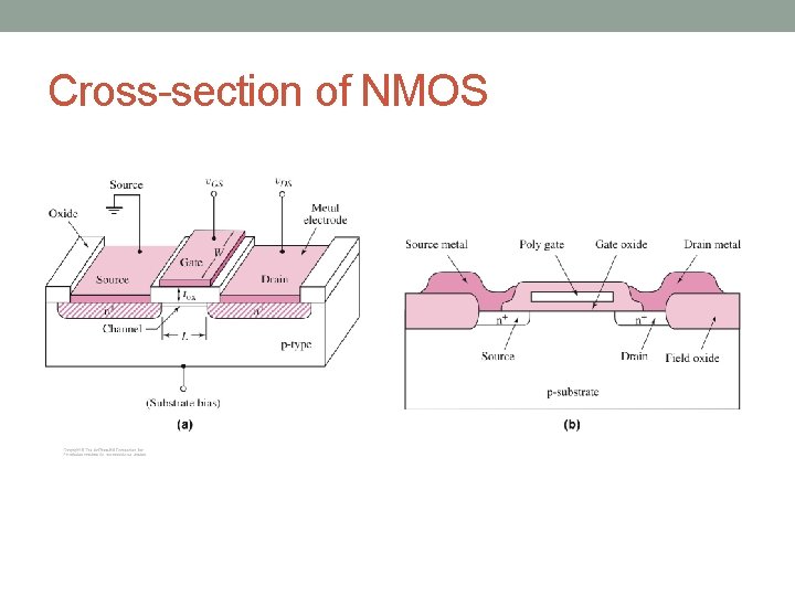
Cross-section of NMOS

Basic Operation Before electron inversion layer is formed After electron inversion layer is formed

Basic Operation

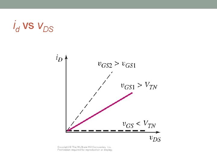
id vs v. DS

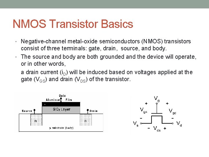
NMOS Transistor Basics • Negative-channel metal-oxide semiconductors (NMOS) transistors consist of three terminals: gate, drain, source, and body. • The source and body are both grounded and the device will operate, or in other words, a drain current (i. D) will be induced based on voltages applied at the gate (VGS) and drain (VDS) of the transistor.

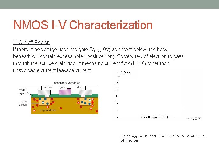
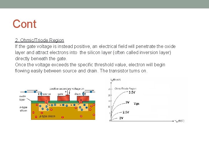
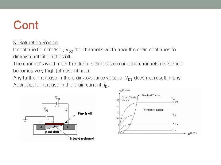
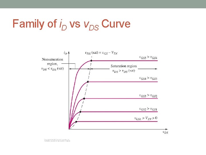
NMOS Transistor Operation • Every NMOS transistor contains a threshold voltage (Vt) which is constant and unique for each transistor. • In order for the transistor to operate, VGS must be greater than Vt. Once this condition has been met, the resulting drain current can be controlled by the voltages supplied at the gate and the drain. • The relationship between VGS, VDS, and i. D is described by three regions of operation: 1. Cut-off Region: In this region no channel exists (i. D = 0) for all values of VD. (VGS < Vt) 2. Ohmic/Triode Region: The NMOS transistor is active and not “pinched off. ” This means the value of VDS affects the value of i. D (VGS > Vt and VDS ≤ VGS – Vt). 3. Saturation Region: The channel is “pinched off” because increases in VD have no affect on ID (VGS > Vt and VDS > VGS – Vt). In the saturation region, the amount of drain current is directly related to the values of VGS > Vt.

NMOS I-V Characterization 1. Cut-off Region If there is no voltage upon the gate (VGS = 0 V) as shows below, the body beneath will contain excess hole ( positive ion). So very few of electron to pass through the source drain gap. It means no current flow (i. D = 0) other than unavoidable current leakage current. Given VGS = 0 V and Vt = 1. 4 V so VGS < Vt : Cutoff region

Cont 2. Ohmic/Triode Region If the gate voltage is instead positive, an electrical field will penetrate the oxide layer and attract electrons into the silicon layer (often called inversion layer) directly beneath the gate. Once the voltage exceeds the specific threshold value, electron will begin flowing easily between source and drain. The transistor turns on.

Cont 3. Saturation Region If continue to increase , VDS the channel’s width near the drain continues to diminish until it pinches off. The channel’s width near the drain is almost zero and the channels resistance becomes very high (almost infinite). Any further increase in the drain-to-source voltage, VDS does not result in any Appreciable increase in the drain current, i. D.

Family of i. D vs v. DS Curve

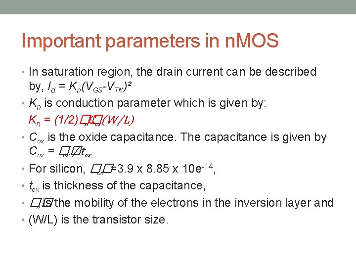
Important parameters in n. MOS • In saturation region, the drain current can be described by, Id = Kn(VGS-VTN)² • Kn is conduction parameter which is given by: Kn = (1/2)�� n. Cox(W/L) • Cox is the oxide capacitance. The capacitance is given by Cox = �� ox / tox -14, • For silicon, �� ox =3. 9 x 8. 85 x 10 e • tox is thickness of the capacitance, • �� n is the mobility of the electrons in the inversion layer and • (W/L) is the transistor size.

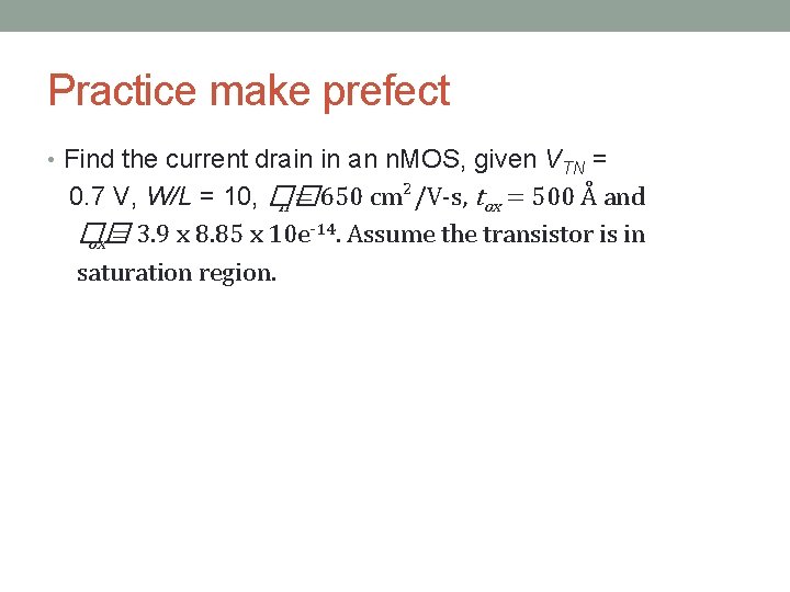
Practice make prefect • Find the current drain in an n. MOS, given VTN = 0. 7 V, W/L = 10, �� n = 650 cm²/V-s, tox = 500 Å and -14 �� ox = 3. 9 x 8. 85 x 10 e. Assume the transistor is in saturation region.