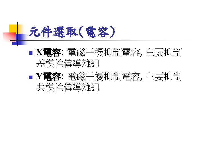
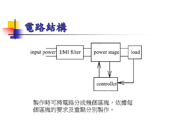
EMI Filter and rectifier circuit EMI Filter Rectifier


: High level two")


")
")
")
- Slides: 43
EMI Filter and rectifier circuit EMI Filter Rectifier circuit
Power stage and control stage
控制IC介紹 UC 3842 Introduction n n Peak current mode control Using to Flyback converter or Forward converter Low start up current UVLO
UC 3842 Ratings
UC 384 X Electrical Characteristics
UC 3842 Applied Circuit
Circuit Configuration with UC 3842
UC 3842 Block Diagram
UC 3842 Oscillator
UC 3842 Error Amp Configuration
UC 3842 Current Sense Circuit
UC 3842 Drive Circuit
UC 3842 Isolated Drive Circuit
UC 3842 Soft-Start Circuit
What is Soft-Start? n When the converter is first switched on, the drive pulses should be progressively increased to allow a slow buildup in output current and voltage. If this soft-start action is not provided, there will be a large inrush current on initial switch-on.
Inrush Current 1. Soft-start 2. A resistive limiting device in series with the supply lines.
TL 494 Introduction n n Voltage mode control PWM IC Double output drive signal High power dissipation Adjustable deadtime control
TL 494 Ratings
TL 494 Applied Circuit
TL 494 Representative Block Diagram
TL 494 Oscillator
TL 494 Timing Diagram
TL 494 Pin Functions n n Pin 13 (output control pin): High level two output transistors alternately for pushpull operation. The output frequency is equal to half that of he oscillator. The duty of output drive signal is less than 0. 5. Low level two output transistors on/off operation. The output frequency is equal to that of he oscillator. The duty of output drive signal is less than 1. Pin 4 (deadtime control pin): Voltage level Duty
TL 494 Error Amp Sense Circuit
TL 494 Deadtime Control Circuit
TL 494 Soft-Start Circuit
TL 494 Output Drive Circuit
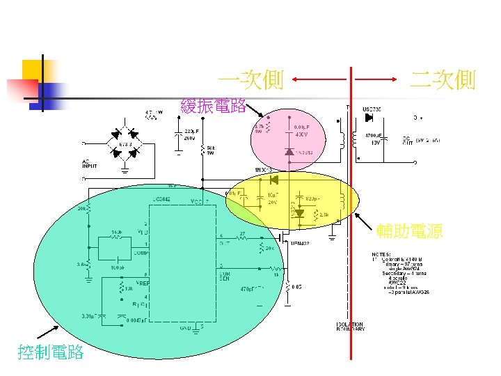
Isolation
Optocoupler Interface Circuit
Overvoltage Protection (I)
Overvoltage Protection (II)
Overvoltage Protection (III)