EME 201 Materials Science Grain Boundaries and Microscopy
EME 201 Materials Science Grain Boundaries and Microscopy
Material Surface - External Surfaces • One of the most prominent boundaries is the outer surface of the crystal structure. • Surface atoms are not tied to the nearest neighbor number and therefore are in a higher energy state than the atoms in the inner state. • The bonds of these unsatisfied surface atoms cause a surface energy expressed in units of energy per unit area (J / m 2). • To reduce this energy, materials tend to reduce the total surface area to the minimum if possible. • Surface imperfections are boundaries or planes that divide a material into zones; each region has the same crystal structure but with different orientations. • These defects include outer surfaces, grain boundaries, phase boundaries, twin boundaries, and stacking faults.
Grain Boundaries • The microstructure of many engineering materials, ceramics and metalls, are composed of many grains. • The grain is a piece of crystalline material in which the order of the atoms is almost the same. • However, the direction of the crystal structure or of the atomic order is different in each adjacent sequence. • A grain boundary separating individual grains is a narrow zone where the atoms are not uniformly spaced. • In other words, the atoms cause a compression zone because they are very close to each other in some places on the grain boundary, and they cause a tension zone because they are too far away from other areas.
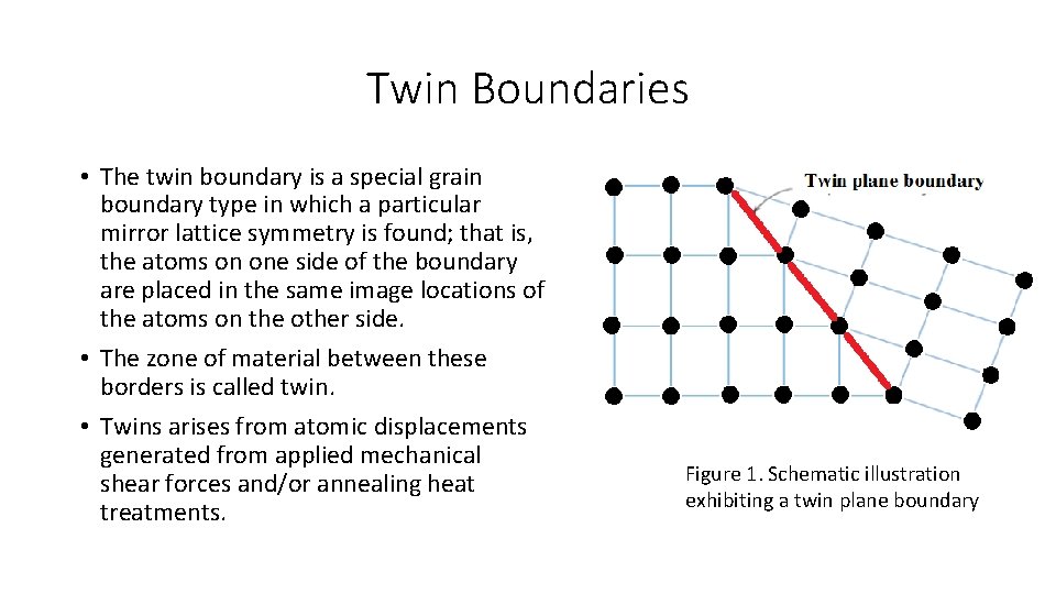
Twin Boundaries • The twin boundary is a special grain boundary type in which a particular mirror lattice symmetry is found; that is, the atoms on one side of the boundary are placed in the same image locations of the atoms on the other side. • The zone of material between these borders is called twin. • Twins arises from atomic displacements generated from applied mechanical shear forces and/or annealing heat treatments. Figure 1. Schematic illustration exhibiting a twin plane boundary
ATOMIC VIBRATIONS • Every atom within the solid material vibrates very quickly around the lattice position in the crystal. • In a manner of speaking, these atomic vibrations can be thought of as imperfections. • At any given moment, all atoms do not oscillate with the same frequency and amplitude or with the same energy. • At a given temperature, there is an energy distribution for the constituent atoms about an average energy. • If we rise the temperature, this average energy also grows up. • Actually, a solid temperature is only a measure of the average vibrational activity of atoms and molecules. • For example, melting occurs when vibrations are large enough to pull off atomic bonds.
MICROSCOPIC TECHNIQUES • Optical microscopy is a simple image analysis technique to investigate the sample surfaces. • Optical microscopy is a technique used to bring to light the microstructural features like grain boundaries requiring less than about 2000 magnifications. • For visible light opaque materials (all metallic materials, many ceramic materials and polymeric materials) only the surface is observed and the light microscope should be used in a reflective mode. • The process of preparing a metallic sample for image analysis, and observing or recording the metal structure is called metallography. • The material sample is sanded and turned into a mirror-like lacquer.
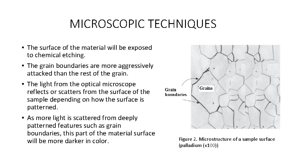
MICROSCOPIC TECHNIQUES • The surface of the material will be exposed to chemical etching. • The grain boundaries are more aggressively attacked than the rest of the grain. • The light from the optical microscope reflects or scatters from the surface of the sample depending on how the surface is patterned. • As more light is scattered from deeply patterned features such as grain boundaries, this part of the material surface will be more darker in color. Figure 2. Microstructure of a sample surface (palladium (x 100))
Electron Microscopy • The upper limit for possible magnification with an optical microscope is about 2000 x. • As a result, some structural items are too thin or too small to allow observation using optical microscopy. • In such cases, an electron microscope with higher magnification capacity can be used. • An image of the studied structure was created using electron beams instead of light radiation. • The high magnification and resolution of these microscopes are the result of the short wave lengths of the electron beams. • The geometry of the microscope components is the same as in optical systems.
Electron Microscopy • Both reflection and transmission beam modes of operation are possible in electron microscopes. • There are two types of microscopy techniques depending on the operation modes. • Transmission Electron Microscopy Technique • The image obtained by a transmission electron microscope (TEM) is created by an electron beam passing the sample. • Scanning Electron Microscopy Technique • The surface of a sample to be investigated is scanned by an electron beam and the reflected electron beam is collected and then shown on a cathode ray tube. • The picture taken on the screen shows the surface properties of the sample.
REFERENCES • William D. Callister, ‘Materials Science and Engineering: An Introduction’, Seventh edition, John Wiley & Sons, Inc. , U. S. A. • Brian S. Mitchell, ‘AN INTRODUCTION TO MATERIALS ENGINEERING AND SCIENCE FOR CHEMICAL AND MATERIALS ENGINEERS’, John Wiley & Sons, Inc. , U. S. A, 2004. • J. W. Martin, ‘Materials for Engineering’, Third Edition, WOODHEAD PUBLISHING LIMITED, Cambridge, England. • Donald R. Askeland & Pradeep P. Fulay, ‘Essentials of Materials Science and Engineering’, Second Edition, Cengage Learning, Toronto, Canada. • G. S. Brady, H. R. Clauser, J. A. Vaccari, ‘Materials Handbook’, Fifteenth Edition, Mc. Graw-Hill Handbooks.
- Slides: 10