EMC design guidelines applied to electronic circuit Or
- Slides: 40

EMC design guidelines applied to electronic circuit Or try to find your EMC ennemy to choose the appropriate way to kill it Sébastien Girard Université Clermont Auvergne Institut Pascal Sebastien. girard@uca. fr 1

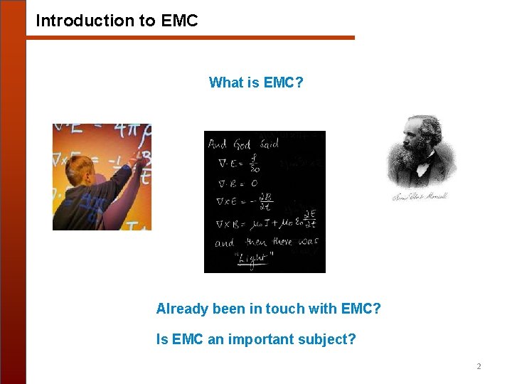
Introduction to EMC What is EMC? Already been in touch with EMC? Is EMC an important subject? 2

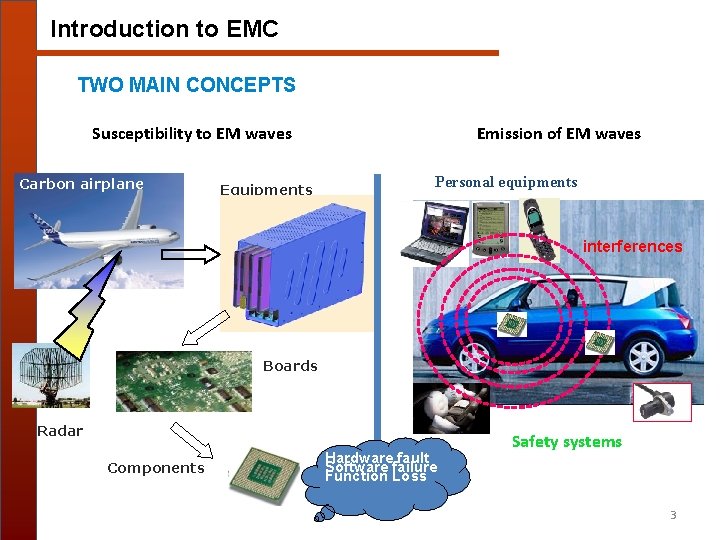
Introduction to EMC TWO MAIN CONCEPTS Susceptibility to EM waves Carbon airplane Equipments Emission of EM waves Personal equipments interferences Boards Radar Components Hardware fault Software failure Function Loss Safety systems 3

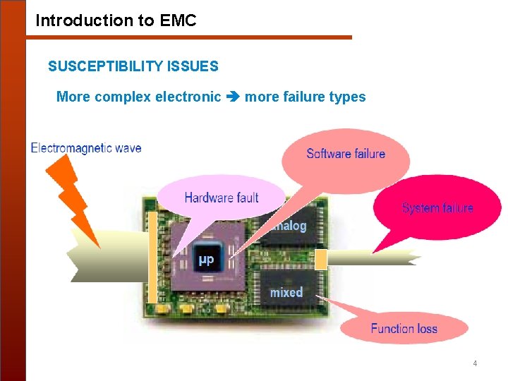
Introduction to EMC SUSCEPTIBILITY ISSUES More complex electronic more failure types 4

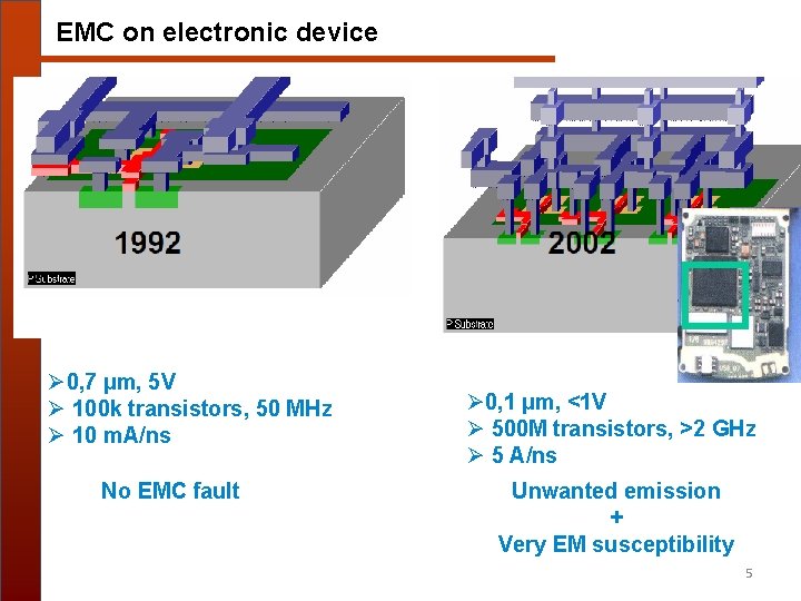
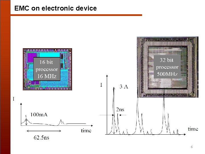
EMC on electronic device Ø 0, 7 µm, 5 V Ø 100 k transistors, 50 MHz Ø 10 m. A/ns No EMC fault Ø 0, 1 µm, <1 V Ø 500 M transistors, >2 GHz Ø 5 A/ns Unwanted emission + Very EM susceptibility 5

EMC on electronic device 6

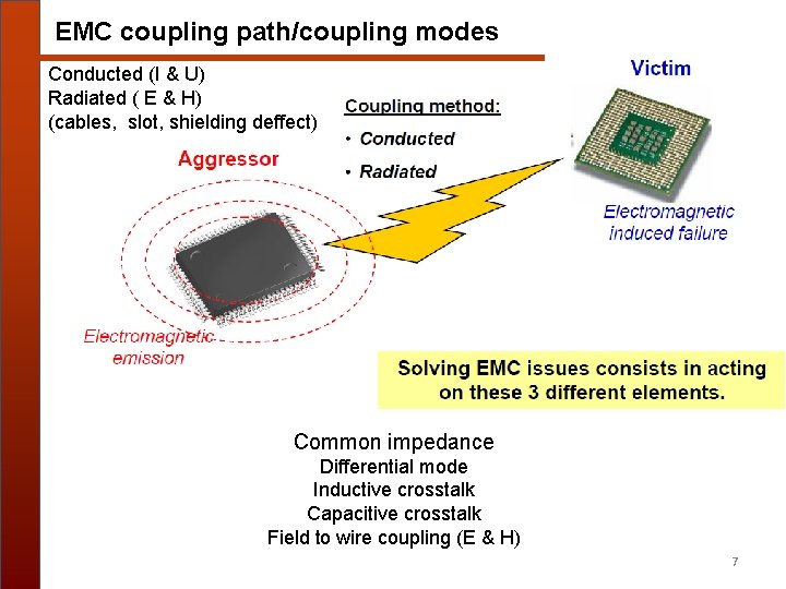
EMC coupling path/coupling modes Conducted (I & U) Radiated ( E & H) (cables, slot, shielding deffect) Common impedance Differential mode Inductive crosstalk Capacitive crosstalk Field to wire coupling (E & H) 7

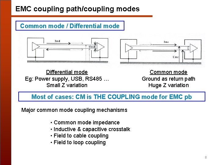
EMC coupling path/coupling modes Common mode / Differential mode Eg: Power supply, USB, RS 485 … Small Z variation Common mode Ground as return path Huge Z variation Most of cases: CM is THE COUPLING mode for EMC pb Major common mode coupling mechanisms • Common mode impedance • Inductive & capacitive crosstalk • Field to cable coupling • Field to loop coupling 8

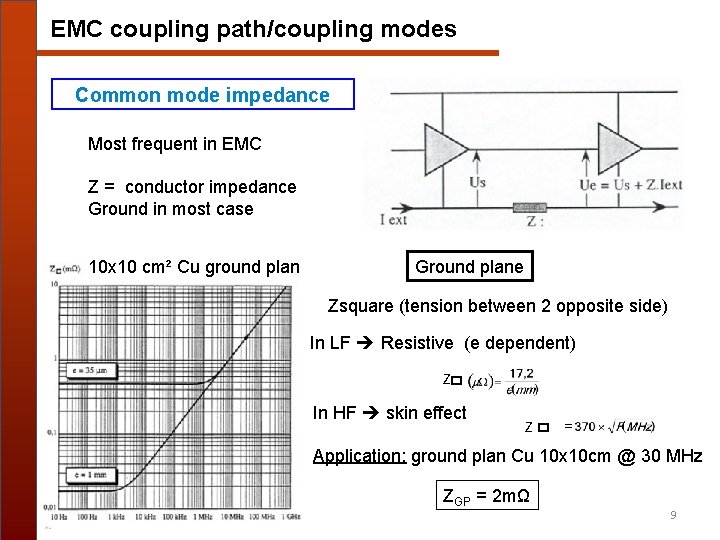
EMC coupling path/coupling modes Common mode impedance Most frequent in EMC Z = conductor impedance Ground in most case 10 x 10 cm² Cu ground plan Ground plane Zsquare (tension between 2 opposite side) In LF Resistive (e dependent) Z In HF skin effect Z = Application: ground plan Cu 10 x 10 cm @ 30 MHz ZGP = 2 mΩ 9

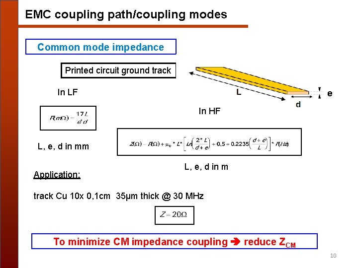
EMC coupling path/coupling modes Common mode impedance Printed circuit ground track In LF e In HF L, e, d in mm Application: L, e, d in m track Cu 10 x 0, 1 cm 35µm thick @ 30 MHz To minimize CM impedance coupling reduce ZCM 10

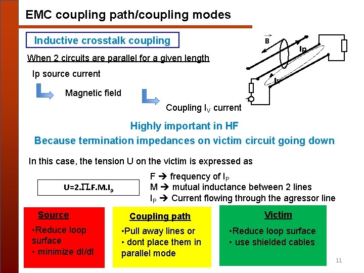
EMC coupling path/coupling modes Inductive crosstalk coupling B Ip When 2 circuits are parallel for a given length Ip source current Iv Magnetic field Coupling IV current Highly important in HF Because termination impedances on victim circuit going down In this case, the tension U on the victim is expressed as U=2. P. F. M. Ip Source • Reduce loop surface • minimize d. I/dt F frequency of IP M mutual inductance between 2 lines IP Current flowing through the agressor line Coupling path • Pull away lines or • dont place them in parallel mode Victim • Reduce loop surface • use shielded cables 11

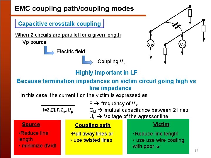
EMC coupling path/coupling modes Capacitive crosstalk coupling When 2 circuits are parallel for a given length Vp source Vp Vv Electric field Coupling VV Highly important in LF Because termination impedances on victim circuit going high vs line impedance In this case, the current I on the victim is expressed as I=2. P. F. Cm. Up Source • Reduce line length • minimize d. V/dt F frequency of VP CM mutual capacitance between 2 lines UP Voltage of the agressor line Coupling path • Pull away lines or • use twisted lines Victim • Reduce line length • use wire coating with poor er 12

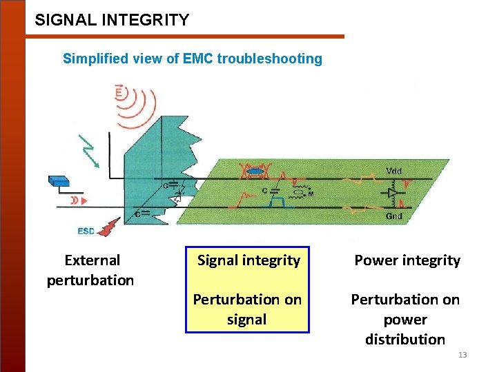
SIGNAL INTEGRITY Simplified view of EMC troubleshooting External perturbation Signal integrity Power integrity Perturbation on signal Perturbation on power distribution 13

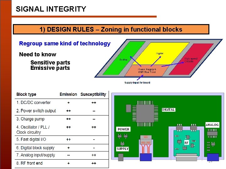
SIGNAL INTEGRITY 1) DESIGN RULES – Zoning in functional blocks Regroup same kind of technology Need to know Sensitive parts Emissive parts 14

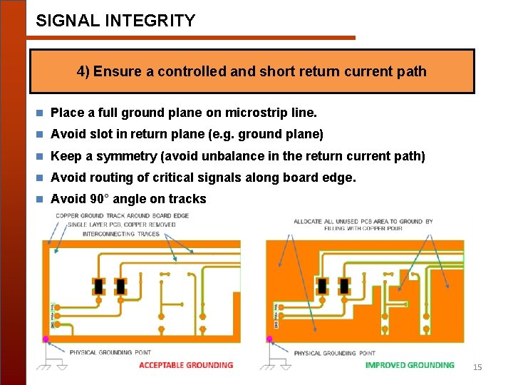
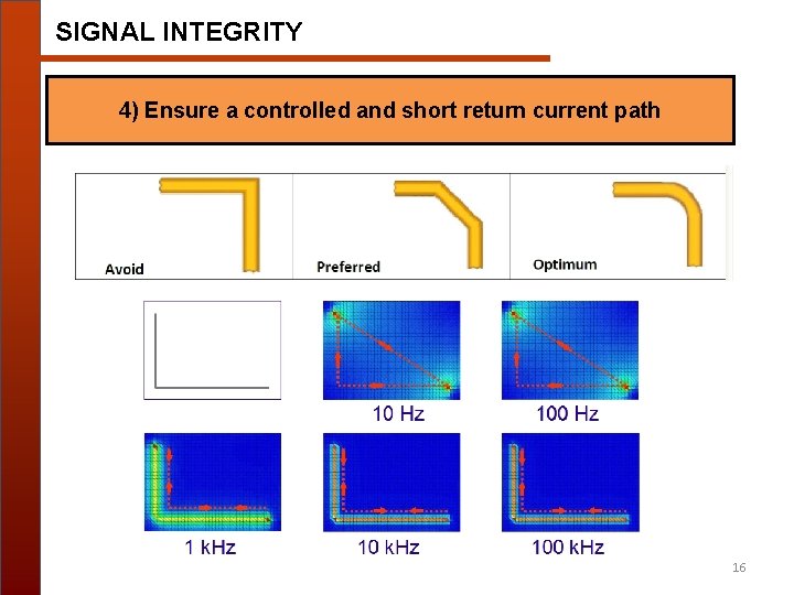
SIGNAL INTEGRITY 4) Ensure a controlled and short return current path n Place a full ground plane on microstrip line. n Avoid slot in return plane (e. g. ground plane) n Keep a symmetry (avoid unbalance in the return current path) n Avoid routing of critical signals along board edge. n Avoid 90° angle on tracks 15

SIGNAL INTEGRITY 4) Ensure a controlled and short return current path 16

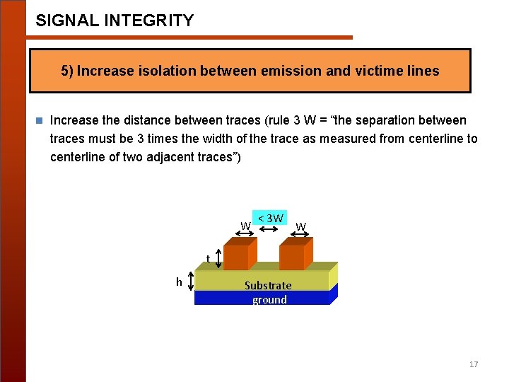
SIGNAL INTEGRITY 5) Increase isolation between emission and victime lines n Increase the distance between traces (rule 3 W = “the separation between traces must be 3 times the width of the trace as measured from centerline to centerline of two adjacent traces”) W < 3 W W t h (εr = 4. 5) Substrate ground 17

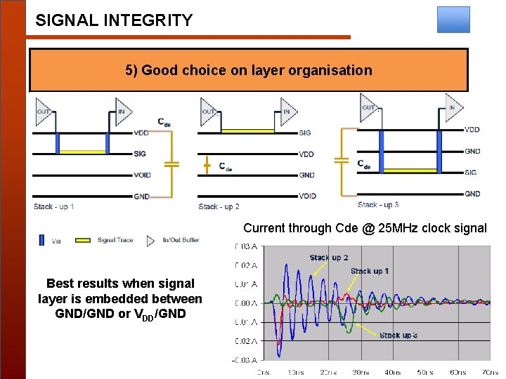
SIGNAL INTEGRITY 5) Good choice on layer organisation Current through Cde @ 25 MHz clock signal Best results when signal layer is embedded between GND/GND or VDD/GND 18

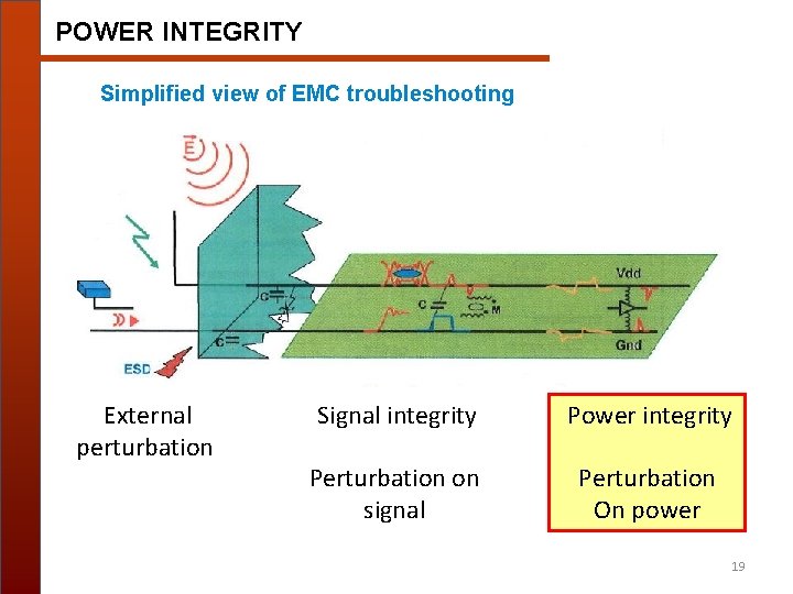
POWER INTEGRITY Simplified view of EMC troubleshooting External perturbation Signal integrity Power integrity Perturbation on signal Perturbation On power 19

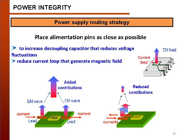
POWER INTEGRITY Power supply routing strategy Place alimentation pins as close as possible to increase decoupling capacitor that reduces voltage fluctuations reduce current loop that generate magnetic field 20

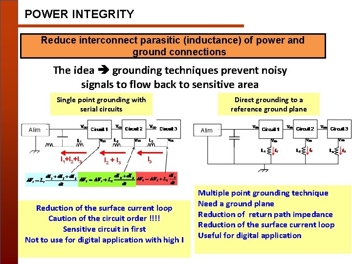
POWER INTEGRITY Reduce interconnect parasitic (inductance) of power and ground connections The idea grounding techniques prevent noisy signals to flow back to sensitive area Single point grounding with serial circuits Direct grounding to a reference ground plane Alim I 1+I 2+I 3 I 2 + I 3 Reduction of the surface current loop Caution of the circuit order !!!! Sensitive circuit in first Not to use for digital application with high I Multiple point grounding technique Need a ground plane Reduction of return path impedance Reduction of the surface current loop Useful for digital application 21

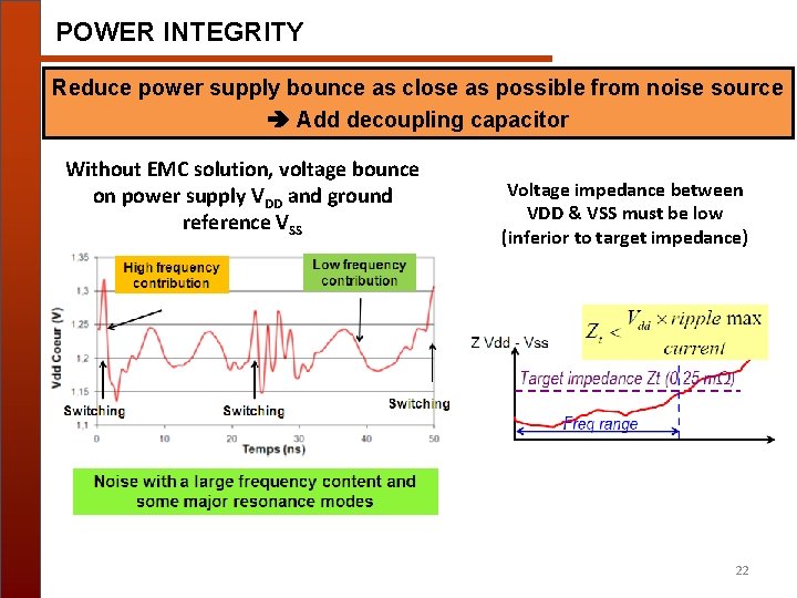
POWER INTEGRITY Reduce power supply bounce as close as possible from noise source Add decoupling capacitor Without EMC solution, voltage bounce on power supply VDD and ground reference VSS Voltage impedance between VDD & VSS must be low (inferior to target impedance) 22

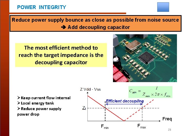
POWER INTEGRITY Reduce power supply bounce as close as possible from noise source Add decoupling capacitor The most efficient method to reach the target impedance is the decoupling capacitor ØKeep current flow internal ØLocal energy tank ØReduce power supply power drop Freq Fmin Fmax 23

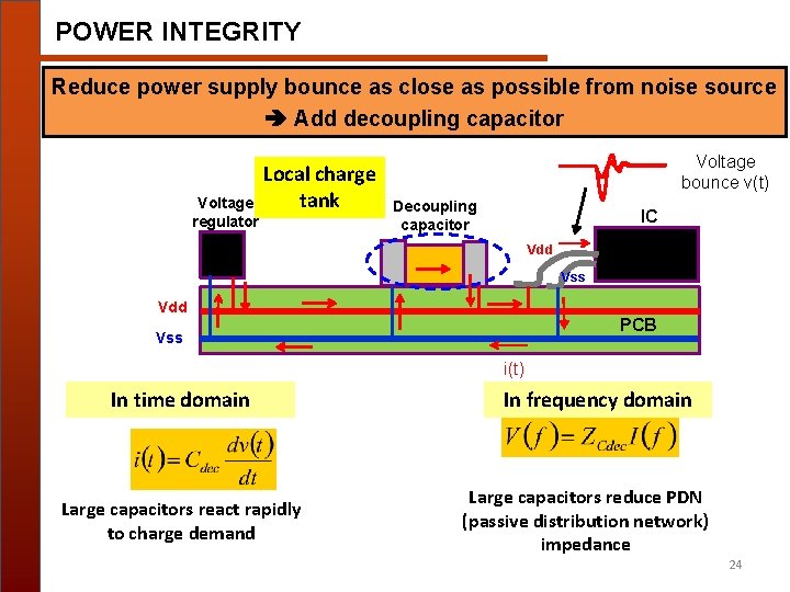
POWER INTEGRITY Reduce power supply bounce as close as possible from noise source Add decoupling capacitor Voltage regulator Local charge tank Voltage bounce v(t) Decoupling capacitor IC Vdd Vss Vdd PCB Vss i(t) In time domain Large capacitors react rapidly to charge demand In frequency domain Large capacitors reduce PDN (passive distribution network) impedance 24

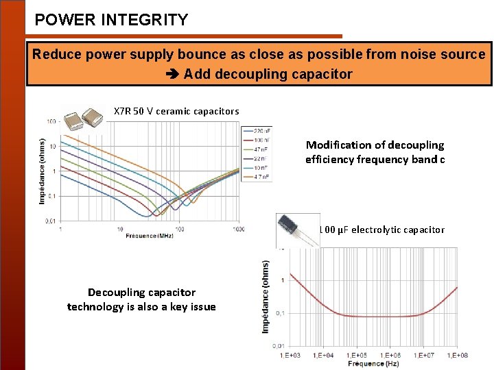
POWER INTEGRITY Reduce power supply bounce as close as possible from noise source Add decoupling capacitor X 7 R 50 V ceramic capacitors Modification of decoupling efficiency frequency band c 100 µF electrolytic capacitor Decoupling capacitor technology is also a key issue 25

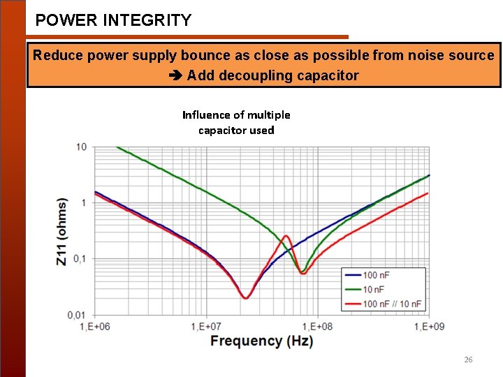
POWER INTEGRITY Reduce power supply bounce as close as possible from noise source Add decoupling capacitor Influence of multiple capacitor used 26

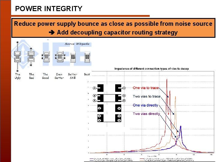
POWER INTEGRITY Reduce power supply bounce as close as possible from noise source Add decoupling capacitor routing strategy 27

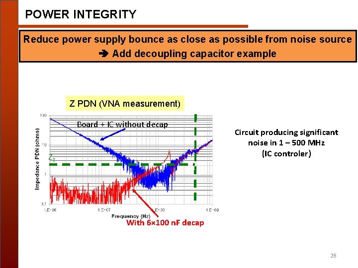
POWER INTEGRITY Reduce power supply bounce as close as possible from noise source Add decoupling capacitor example Z PDN (VNA measurement) Board + IC without decap ZT Circuit producing significant noise in 1 – 500 MHz (IC controler) With 6× 100 n. F decap 28

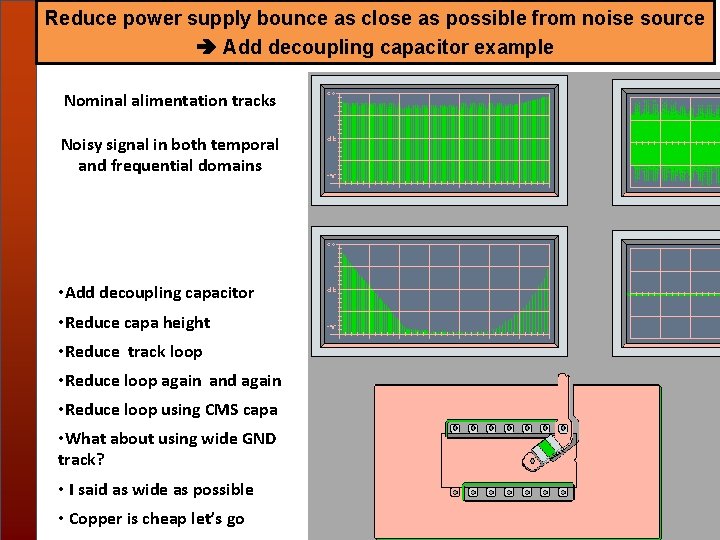
Reduce power supply bounce as close as possible from noise source POWER INTEGRITY Add decoupling capacitor example Nominal alimentation tracks Noisy signal in both temporal and frequential domains • Add decoupling capacitor • Reduce capa height • Reduce track loop • Reduce loop again and again • Reduce loop using CMS capa • What about using wide GND track? • I said as wide as possible • Copper is cheap let’s go 29

CONCLUSION Thanks to all And have fun with EMC 30

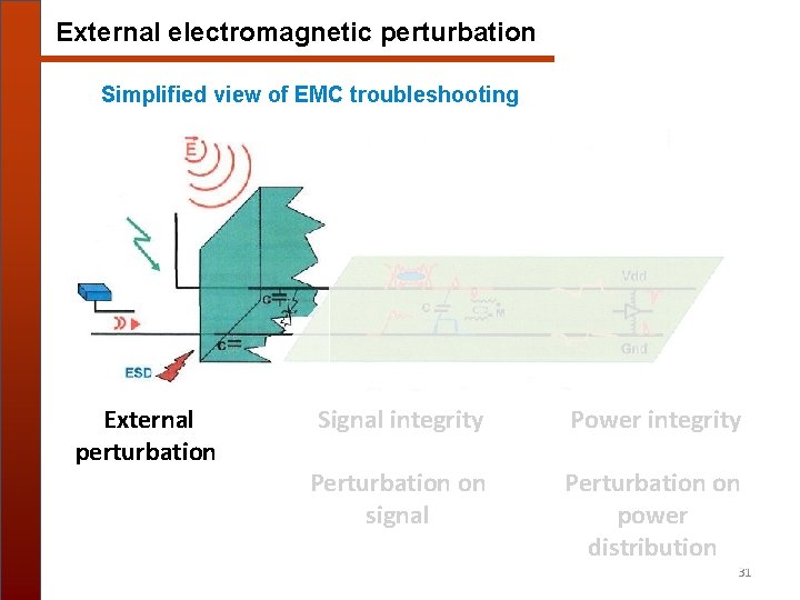
External electromagnetic perturbation Simplified view of EMC troubleshooting External perturbation Signal integrity Power integrity Perturbation on signal Perturbation on power distribution 31

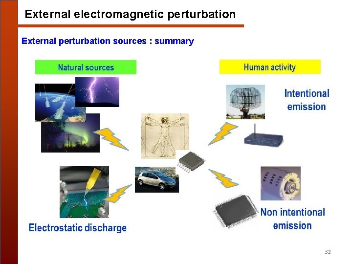
External electromagnetic perturbation External perturbation sources : summary 32

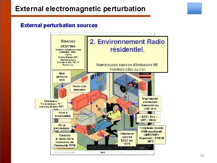
External electromagnetic perturbation External perturbation sources 33

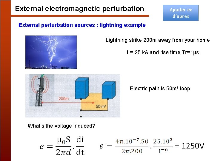
External electromagnetic perturbation Ajouter ex d’apres External perturbation sources : lightning example Lightning strike 200 m away from your home I = 25 k. A and rise time Tr=1µs Electric path is 50 m² loop What’s the voltage induced? 34

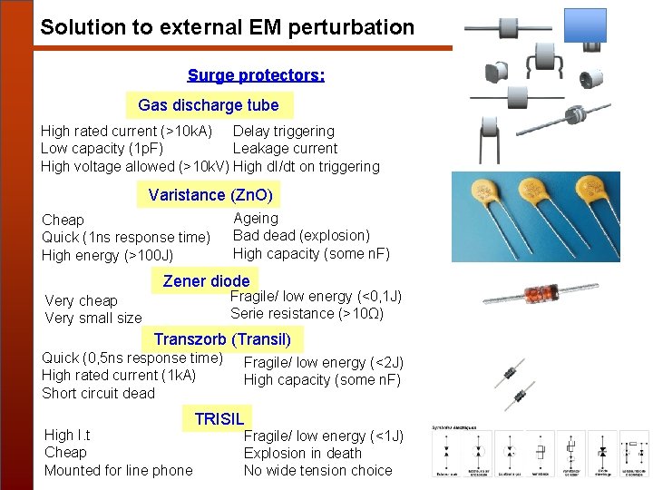
Solution to external EM perturbation Surge protectors: Gas discharge tube High rated current (>10 k. A) Delay triggering Low capacity (1 p. F) Leakage current High voltage allowed (>10 k. V) High d. I/dt on triggering Varistance (Zn. O) Cheap Quick (1 ns response time) High energy (>100 J) Ageing Bad dead (explosion) High capacity (some n. F) Zener diode Fragile/ low energy (<0, 1 J) Serie resistance (>10Ω) Very cheap Very small size Transzorb (Transil) Quick (0, 5 ns response time) High rated current (1 k. A) Short circuit dead High I. t Cheap Mounted for line phone Fragile/ low energy (<2 J) High capacity (some n. F) TRISIL Fragile/ low energy (<1 J) Explosion in death No wide tension choice 35

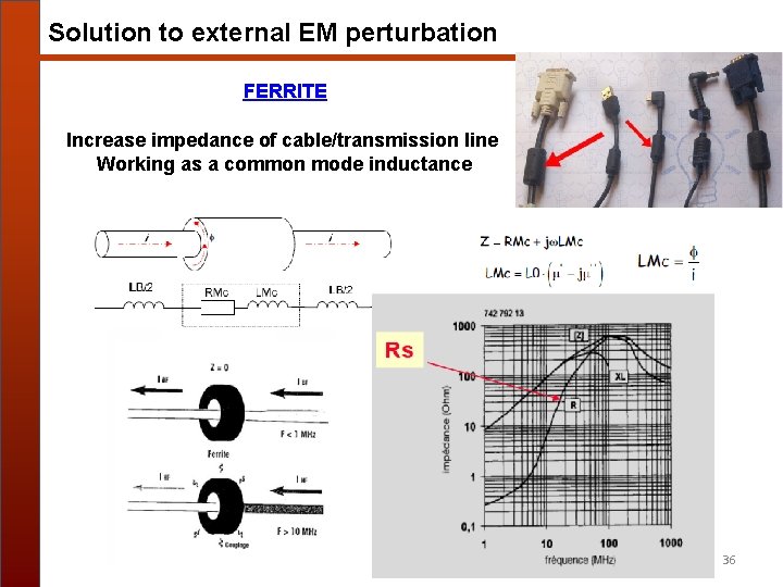
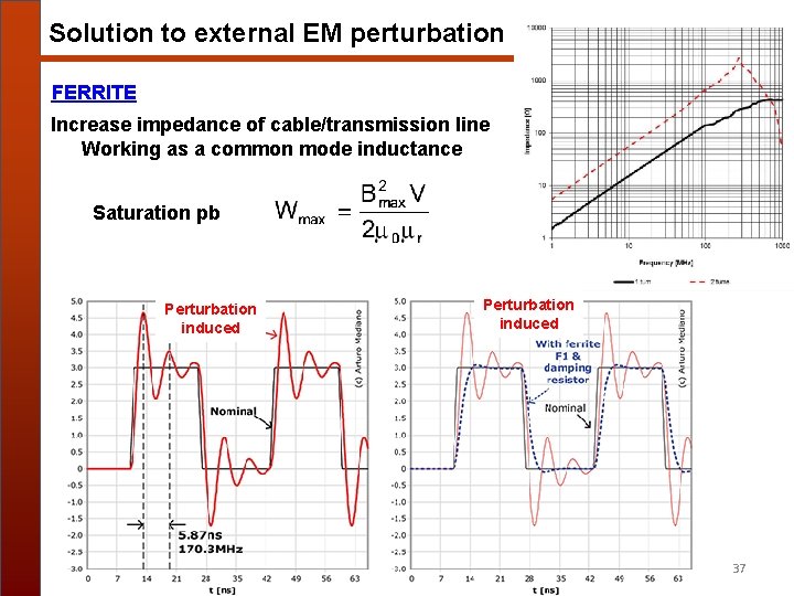
Solution to external EM perturbation FERRITE Increase impedance of cable/transmission line Working as a common mode inductance 36

Solution to external EM perturbation FERRITE Increase impedance of cable/transmission line Working as a common mode inductance Saturation pb Perturbation induced 37

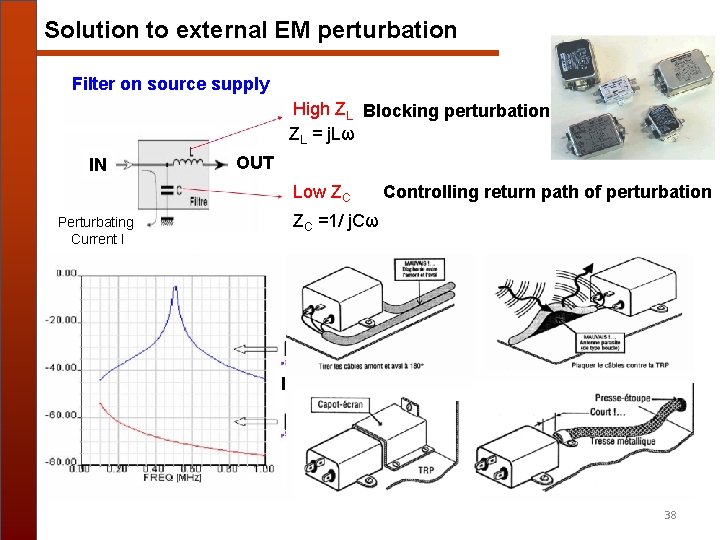
Solution to external EM perturbation Filter on source supply High ZL Blocking perturbation ZL = j. Lω IN OUT Low ZC Perturbating Current I Controlling return path of perturbation ZC =1/ j. Cω IN OUT 38

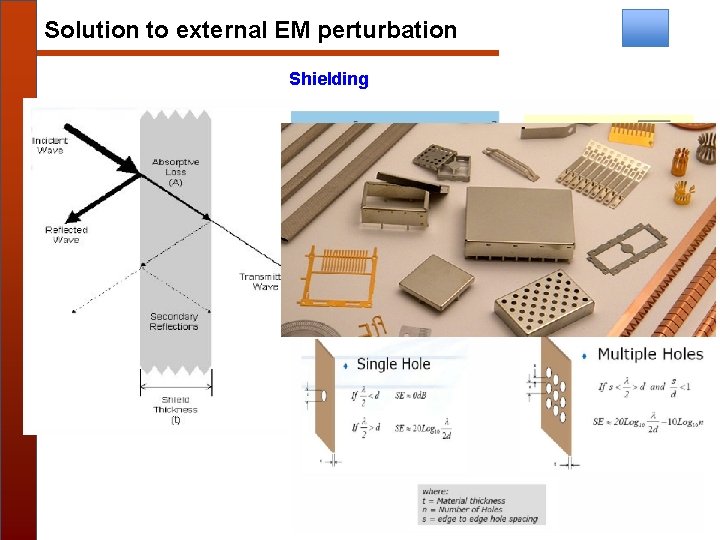
Solution to external EM perturbation Shielding 39

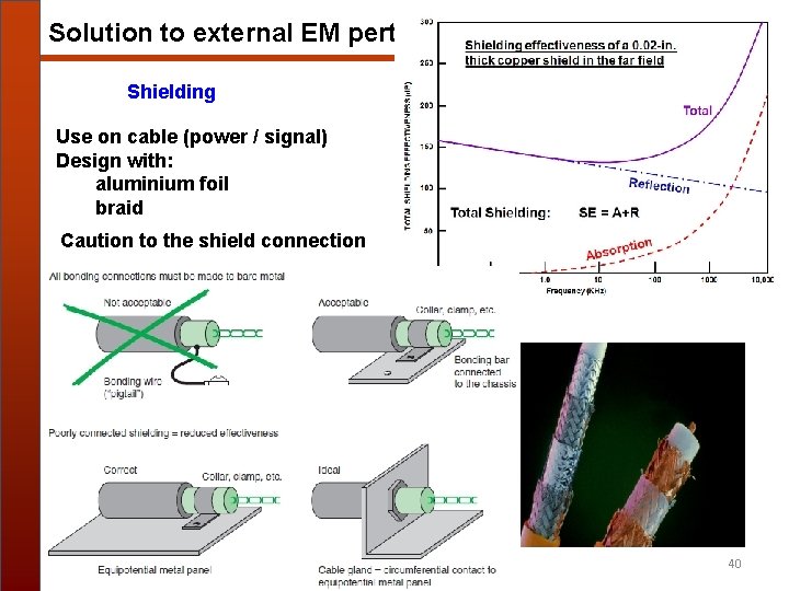
Solution to external EM perturbation Shielding Use on cable (power / signal) Design with: aluminium foil braid Caution to the shield connection 40