Embedded Systems Lab 1 Timers and PWM Dr

Embedded Systems Lab 1 Timers and PWM Dr. Yifeng Zhu Electrical and Computer Engineering University of Maine Fall 2019 1

Timer Free-run counter (independent of processor) � Functions � � � 2 Input capture Output compare Pulse-width modulation (PWM) generation One-pulse mode output

Timer: Clock Reload Value ARR Reload f. CL_PSC clock 3 PSC Prescaler f. CL_CNT Timer Counter ISR Interrupt

Timer: Output ARR Reload Value Reload f. CL_PSC clock PSC f. CL_CNT Timer Counter ISR Interrupt Prescaler = Compare & Capture Register (CCR) 4 Timer Output (OCREF)

Timer: Input Capture Reload Value ARR Reload f. CL_PSC clock PSC f. CL_CNT Timer Counter Prescaler Compare & Capture Register (CCR) 5 ISR Interrupt
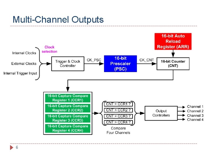
Multi-Channel Outputs 6

Output Compare Mode (OCM) 000 001 010 011 100 101 7 Timer Output (OCREF) Frozen High if CNT == CCR Low if CNT == CCR Toggle if CNT == CCR Forced low (always low) Forced high (always high)
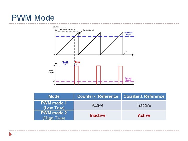
PWM Mode PWM mode 1 (Low True) PWM mode 2 (High True) 8 Counter < Reference Counter ≥ Reference Active Inactive Active
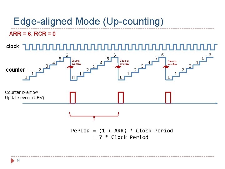
Edge-aligned Mode (Up-counting) ARR = 6, RCR = 0 clock counter 0 1 2 3 4 5 6 Counter overflow 0 Counter overflow Update event (UEV) Period = (1 + ARR) * Clock Period = 7 * Clock Period 9 1 2 3 4 5 6

Edge-aligned Mode (down-counting) ARR = 6, RCR = 0 Clock 6 5 6 4 Counter 3 2 1 0 5 Counter underflow 6 4 3 2 1 Counter underflow 0 Counter underflow Update event (UEV) Period = (1 + ARR) * Clock Period = 7 * Clock Period 10 5 4 3 2 1 0

Center-aligned Mode ARR = 6, RCR = 0 Clock Counter 0 1 2 3 4 5 6 5 4 Counter overflow 3 2 1 0 1 Counter underflow Update event (UEV) Period = 2 * ARR * Clock Period = 12 * Clock Period 11 2 3 4 5 6 5 4 Counter overflow 3 2 1 0 Counter underflow

Mode 1 Timer Output = PWM Mode 1 (Low. True) High if counter < CCR Low if counter ≥ CCR Upcounting mode, ARR = 6, CCR = 3, RCR = 0 Clock CCR = 3 Counter 0 1 2 4 3 5 6 0 1 2 3 4 5 6 OCREF Duty Cycle = = 12 CCR ARR + 1 3 7 Period = (1 + ARR) * Clock Period = 7 * Clock Period
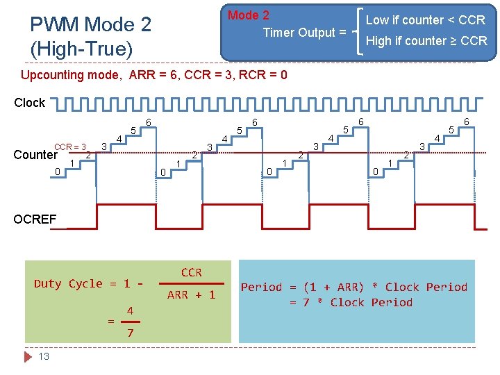
Mode 2 Timer Output = PWM Mode 2 (High-True) Low if counter < CCR High if counter ≥ CCR Upcounting mode, ARR = 6, CCR = 3, RCR = 0 Clock CCR = 3 Counter 0 1 2 4 3 5 6 0 1 2 3 4 5 6 OCREF Duty Cycle = 13 4 7 CCR ARR + 1 Period = (1 + ARR) * Clock Period = 7 * Clock Period
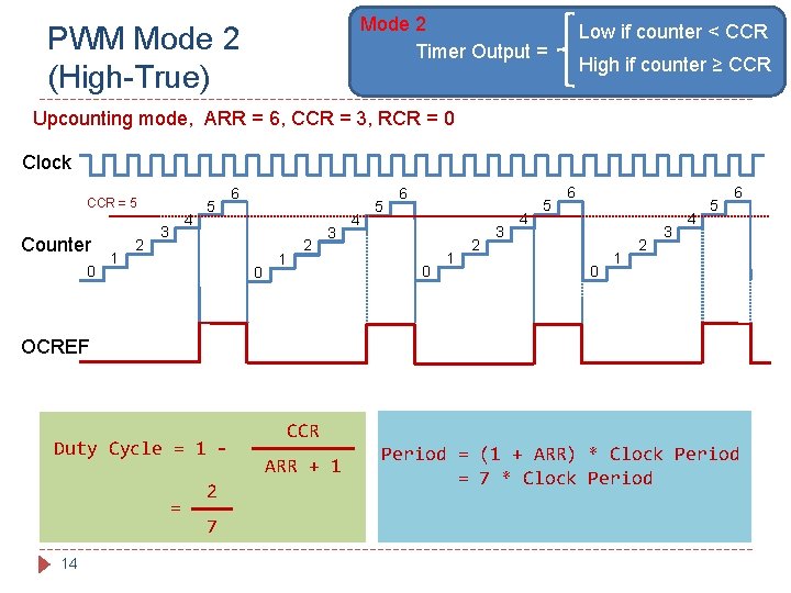
Mode 2 Timer Output = PWM Mode 2 (High-True) Low if counter < CCR High if counter ≥ CCR Upcounting mode, ARR = 6, CCR = 3, RCR = 0 Clock CCR = 5 Counter 0 1 2 4 3 5 6 0 1 2 3 4 5 6 OCREF Duty Cycle = 14 2 7 CCR ARR + 1 Period = (1 + ARR) * Clock Period = 7 * Clock Period
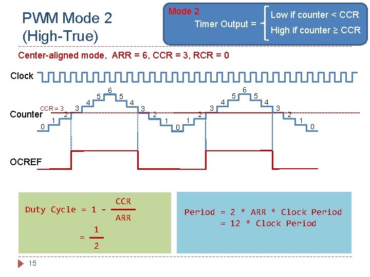
Mode 2 Timer Output = PWM Mode 2 (High-True) Low if counter < CCR High if counter ≥ CCR Center-aligned mode, ARR = 6, CCR = 3, RCR = 0 Clock CCR = 3 Counter 0 1 2 4 3 5 6 5 4 3 2 1 0 1 2 3 4 5 6 5 4 3 2 1 0 OCREF Duty Cycle = 15 1 2 CCR ARR Period = 2 * ARR * Clock Period = 12 * Clock Period
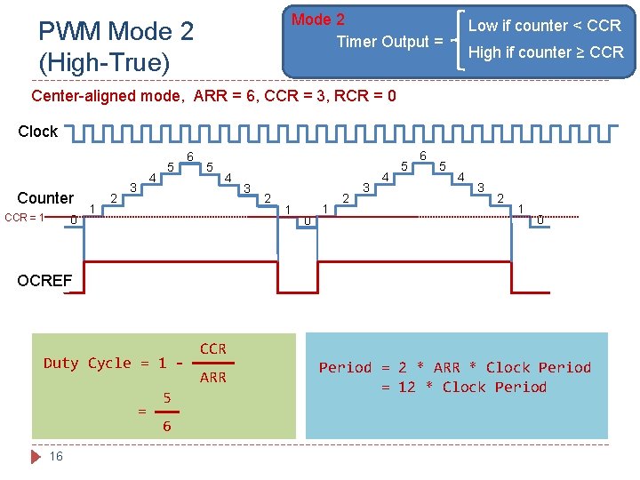
Mode 2 Timer Output = PWM Mode 2 (High-True) Low if counter < CCR High if counter ≥ CCR Center-aligned mode, ARR = 6, CCR = 3, RCR = 0 Clock Counter CCR = 1 0 1 2 4 3 5 6 5 4 3 2 1 0 1 2 3 4 5 6 5 4 3 2 1 0 OCREF Duty Cycle = 16 5 6 CCR ARR Period = 2 * ARR * Clock Period = 12 * Clock Period
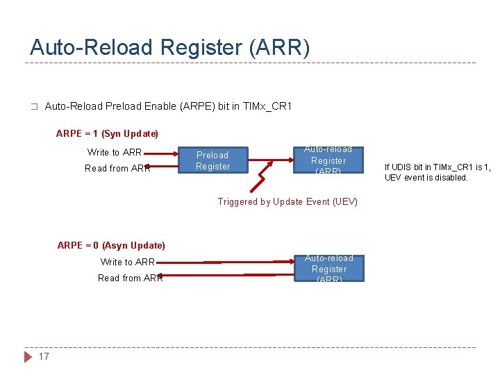
Auto-Reload Register (ARR) � Auto-Reload Preload Enable (ARPE) bit in TIMx_CR 1 ARPE = 1 (Syn Update) Write to ARR Read from ARR Preload Register Auto-reload Register (ARR) Triggered by Update Event (UEV) ARPE = 0 (Asyn Update) Write to ARR Read from ARR 17 Auto-reload Register (ARR) If UDIS bit in TIMx_CR 1 is 1, UEV event is disabled.
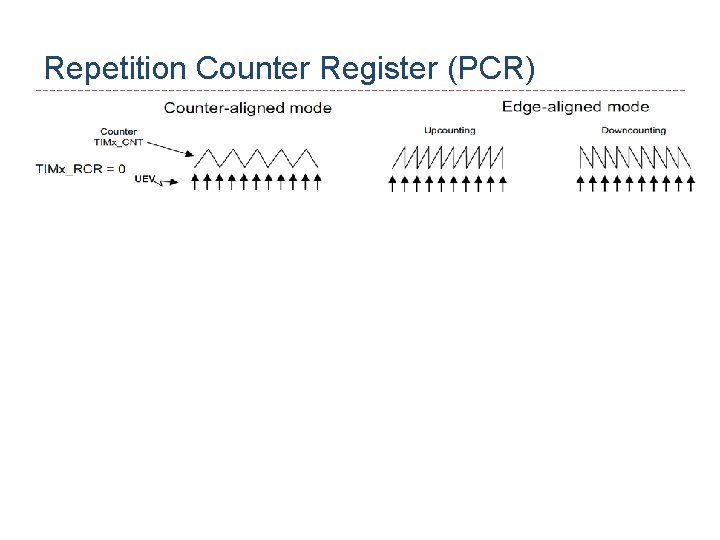
Repetition Counter Register (PCR) 18
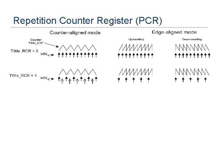
Repetition Counter Register (PCR) 19
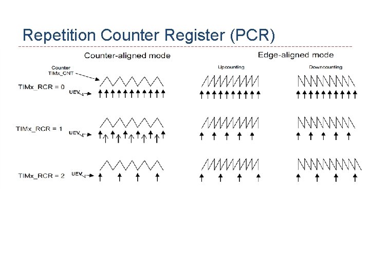
Repetition Counter Register (PCR) 20
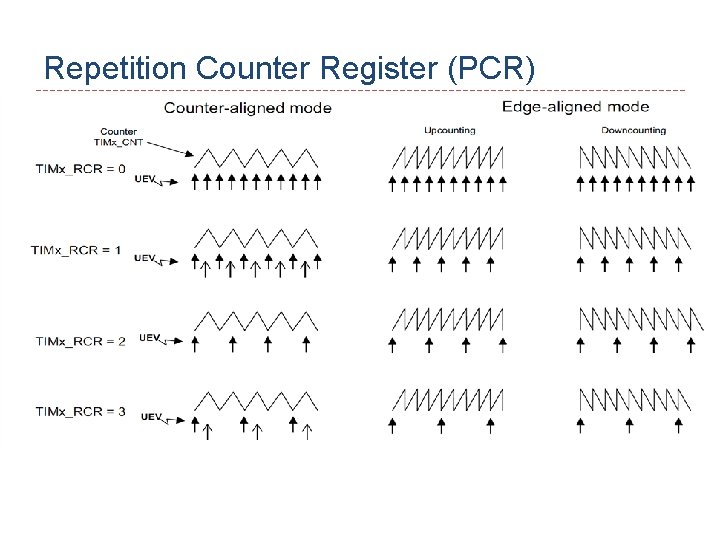
Repetition Counter Register (PCR) 21

Repetition Counter Register (PCR) 22
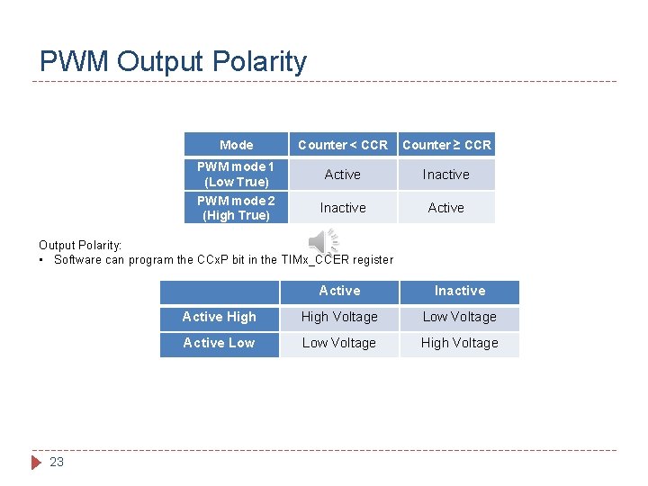
PWM Output Polarity Mode PWM mode 1 (Low True) PWM mode 2 (High True) Counter < CCR Counter ≥ CCR Active Inactive Active Output Polarity: • Software can program the CCx. P bit in the TIMx_CCER register 23 Active Inactive Active High Voltage Low Voltage Active Low Voltage High Voltage
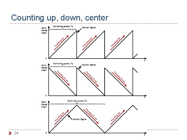
Counting up, down, center 24
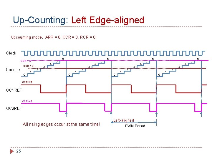
Up-Counting: Left Edge-aligned Upcounting mode, ARR = 6, CCR = 3, RCR = 0 Clock CCR = 6 CCR = 3 Counter 0 1 2 3 4 5 6 0 1 2 3 4 OC 1 REF CCR = 6 OC 2 REF 25 6 0 CCR = 3 All rising edges occur at the same time! 5 Left-aligned PWM Period 1 2 3 4 5 6
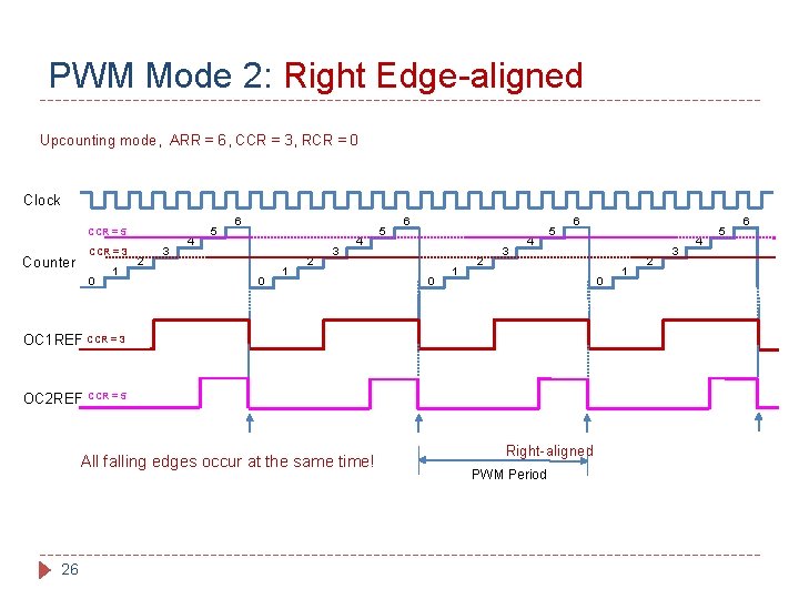
PWM Mode 2: Right Edge-aligned Upcounting mode, ARR = 6, CCR = 3, RCR = 0 Clock CCR = 5 Counter CCR = 3 0 1 2 3 4 5 6 0 OC 1 REF CCR = 3 OC 2 REF CCR = 5 All falling edges occur at the same time! 26 Right-aligned PWM Period 1 2 3 4 5 6
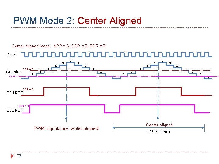
PWM Mode 2: Center Aligned Timer Output = Low if counter < CCR High if counter ≥ CCR Center-aligned mode, ARR = 6, CCR = 3, RCR = 0 Clock Counter CCR = 3 CCR = 1 0 1 2 3 4 5 6 5 4 3 2 1 0 1 2 3 4 5 6 5 CCR = 3 OC 1 REF CCR = 1 OC 2 REF PWM signals are center aligned! 27 Center-aligned PWM Period 4 3 2 1 0
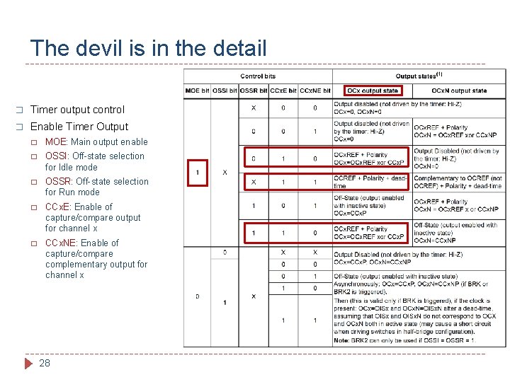
The devil is in the detail � Timer output control � Enable Timer Output � MOE: Main output enable � OSSI: Off-state selection for Idle mode � OSSR: Off-state selection for Run mode � CCx. E: Enable of capture/compare output for channel x � CCx. NE: Enable of capture/compare complementary output for channel x 28
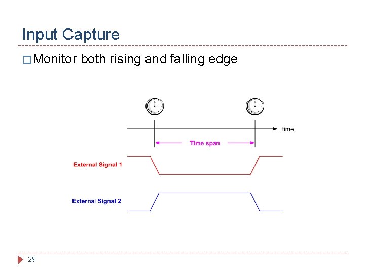
Input Capture � Monitor 29 both rising and falling edge
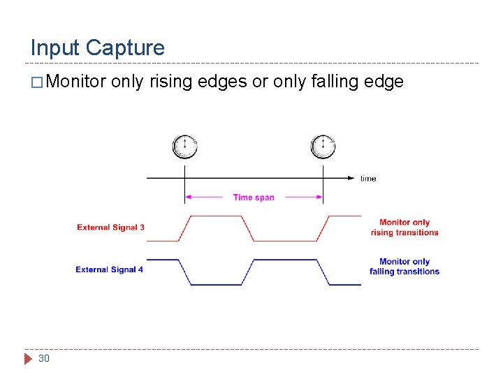
Input Capture � Monitor 30 only rising edges or only falling edge
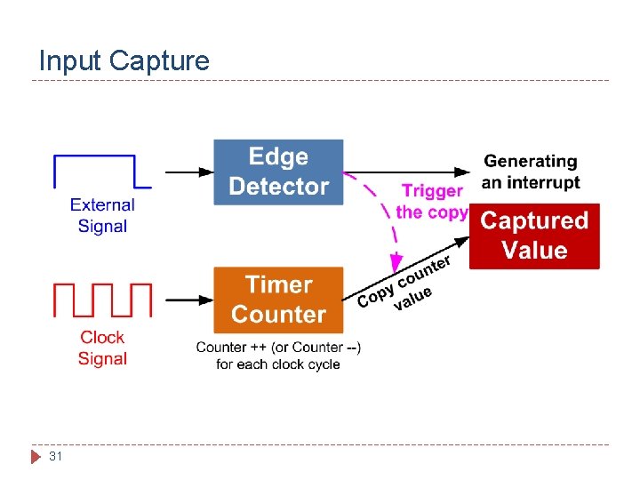
Input Capture 31
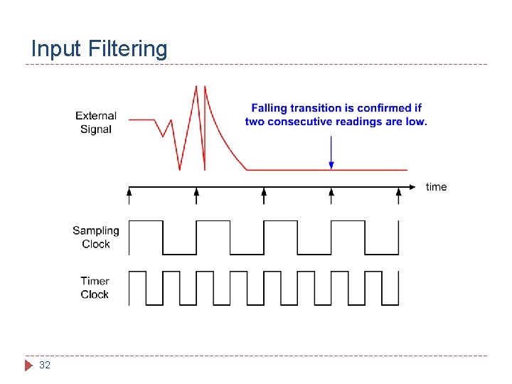
Input Filtering 32
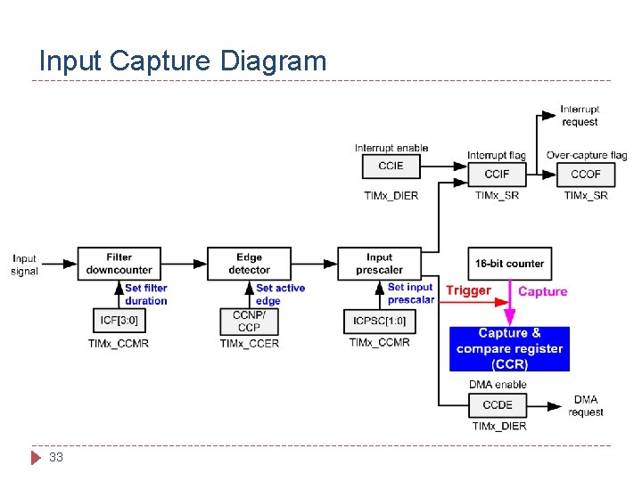
Input Capture Diagram 33

Intro to the STEVAL Drone Kit: � The STEVAL-DRONE 01 is a drone kit with fully functional open source code libraries 34
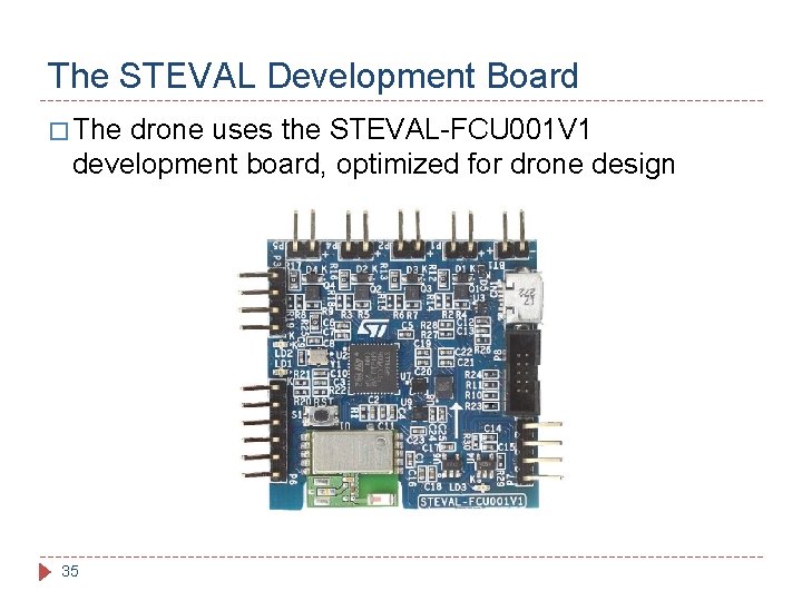
The STEVAL Development Board � The drone uses the STEVAL-FCU 001 V 1 development board, optimized for drone design 35
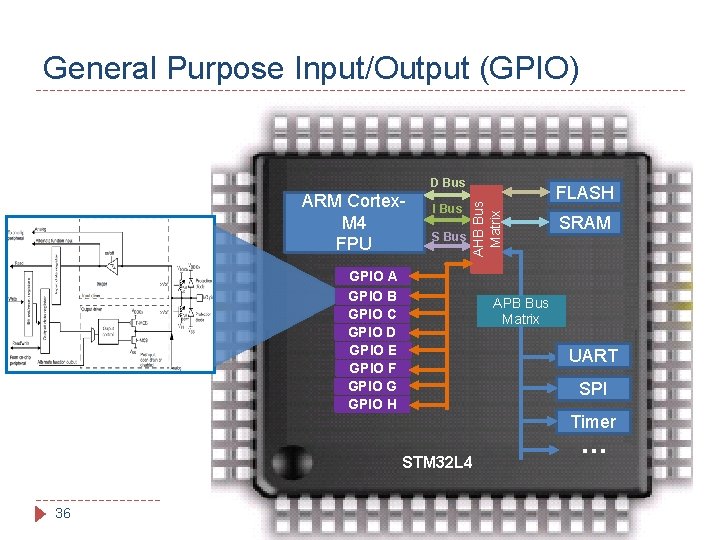
General Purpose Input/Output (GPIO) ARM Cortex. M 4 FPU I Bus S Bus AHB Bus Matrix D Bus GPIO A GPIO B GPIO C GPIO D GPIO E GPIO F GPIO G GPIO H SRAM APB Bus Matrix UART SPI Timer STM 32 L 4 36 FLASH …

General Purpose Input/Output (GPIO) ARM Cortex. M 4 FPU I Bus S Bus AHB Bus Matrix D Bus GPIO A GPIO B GPIO C GPIO D GPIO E GPIO F GPIO G GPIO H SRAM APB Bus Matrix UART SPI Timer STM 32 L 4 37 FLASH …
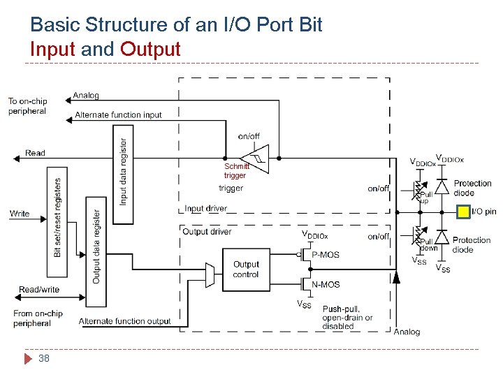
Basic Structure of an I/O Port Bit Input and Output Schmitt trigger 38
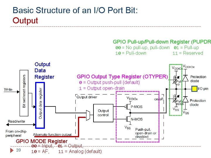
Basic Structure of an I/O Port Bit: Output GPIO Pull-up/Pull-down Register (PUPDR 00 = No pull-up, pull-down 01 = Pull-up 10 = Pull-down 11 = Reserved Output Data Register GPIO MODE Register 39 Schmitt trigger GPIO Output Type Register (OTYPER) 0 = Output push-pull (default) 1 = Output open-drain 00 = Input, 01 = Output, 10 = AF, 11 = Analog (default)

Enable Clock � AHB 2 peripheral clock enable register (RCC_AHB 2 ENR) SYSCLK 1 GPIOEN Clock for Port B AND Gate #define RCC_AHB 2 ENR_GPIOBEN ((uint 32_t)0 x 00000002 U) RCC->AHB 2 ENR |= RCC_AHB 2 ENR_GPIOBEN; 40
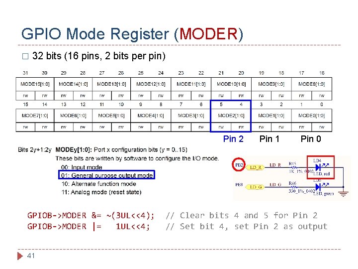
GPIO Mode Register (MODER) � 32 bits (16 pins, 2 bits per pin) Pin 2 GPIOB->MODER &= ~(3 UL<<4); GPIOB->MODER |= 1 UL<<4; 41 Pin 0 // Clear bits 4 and 5 for Pin 2 // Set bit 4, set Pin 2 as output

GPIO Output Type Register (OTYPE) � 16 bits reserved, 16 data bits, 1 bit for each pin GPIOB->OTYPE &= ~(1 UL<<2); 42 // Clear bit 2
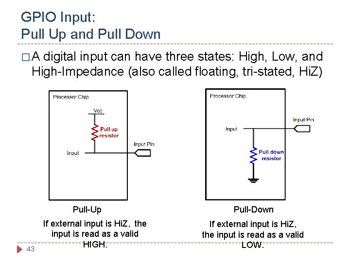
GPIO Input: Pull Up and Pull Down �A digital input can have three states: High, Low, and High-Impedance (also called floating, tri-stated, Hi. Z) Pull-Up 43 If external input is Hi. Z, the input is read as a valid HIGH. Pull-Down If external input is Hi. Z, the input is read as a valid LOW.
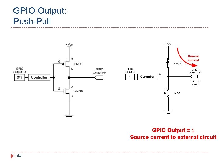
GPIO Output: Push-Pull GPIO Output = 1 Source current to external circuit 44
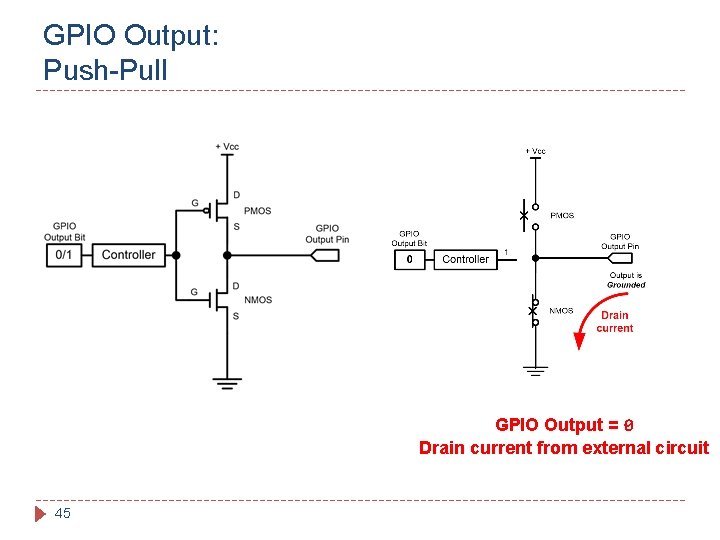
GPIO Output: Push-Pull GPIO Output = 0 Drain current from external circuit 45
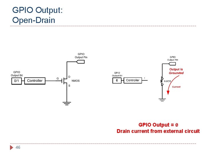
GPIO Output: Open-Drain GPIO Output = 0 Drain current from external circuit 46
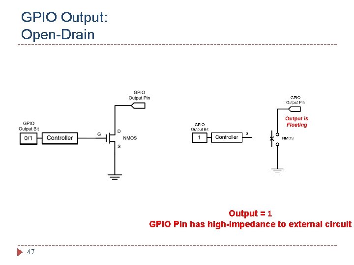
GPIO Output: Open-Drain Output = 1 GPIO Pin has high-impedance to external circuit 47
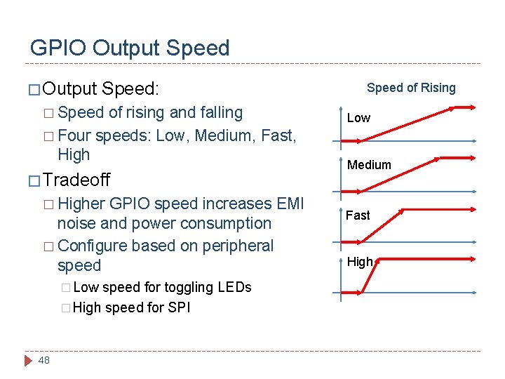
GPIO Output Speed � Output Speed: � Speed of rising and falling � Four speeds: Low, Medium, Fast, High � Tradeoff � Higher GPIO speed increases EMI noise and power consumption � Configure based on peripheral speed � Low speed for toggling LEDs � High speed for SPI 48 Speed of Rising Low Medium Fast High
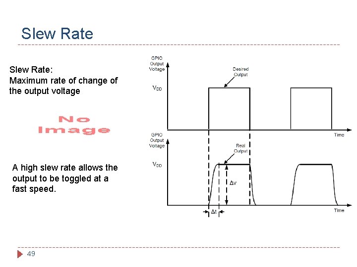
Slew Rate: Maximum rate of change of the output voltage A high slew rate allows the output to be toggled at a fast speed. 49
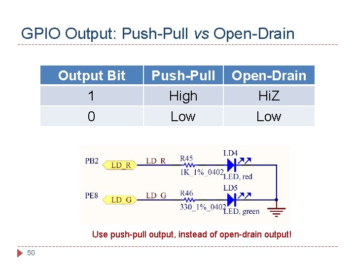
GPIO Output: Push-Pull vs Open-Drain Output Bit 1 Push-Pull High Open-Drain Hi. Z 0 Low Use push-pull output, instead of open-drain output! 50

GPIO Output Data Register (ODR) � 16 bits reserved, 16 data bits, 1 bit for each pin Pin 2 GPIOB->ODR |= 1 UL << 2; 51 // Set bit 2
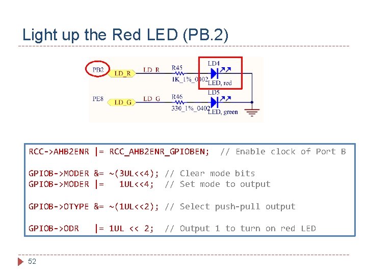
Light up the Red LED (PB. 2) RCC->AHB 2 ENR |= RCC_AHB 2 ENR_GPIOBEN; // Enable clock of Port B GPIOB->MODER &= ~(3 UL<<4); // Clear mode bits GPIOB->MODER |= 1 UL<<4; // Set mode to output GPIOB->OTYPE &= ~(1 UL<<2); // Select push-pull output GPIOB->ODR 52 |= 1 UL << 2; // Output 1 to turn on red LED

GPIO Initialization � Turn on the clock to the GPIO Port (e. g. Port B) RCC->AHBENR |= RCC_AHBENR_GPIOBEN; Reset and Clock Control (RCC) � Configure GPIO mode, output type, speed, pull-up/pull-down 53 typedef struct { __IO uint 32_t MODER; __IO uint 16_t OTYPER; uint 16_t RESERVED 0; __IO uint 32_t OSPEEDR; __IO uint 32_t PUPDR; __IO uint 16_t IDR; uint 16_t RESERVED 1; __IO uint 16_t ODR; uint 16_t RESERVED 2; __IO uint 16_t BSRRL; /* BSRR register is split to 2 * 16 -bit fields BSRRL */ __IO uint 16_t BSRRH; /* BSRR register is split to 2 * 16 -bit fields BSRRH */ __IO uint 32_t LCKR; __IO uint 32_t AFR[2]; } GPIO_Type. Def; #define PERIPH_BASE ((uint 32_t)0 x 40000000) #define AHBPERIPH_BASE (PERIPH_BASE + 0 x 20000) #define GPIOB_BASE (AHBPERIPH_BASE + 0 x 0400) #define GPIOB ((GPIO_Type. Def *) GPIOB_BASE)
GPIO AFR: � The GPIO alternate function mode allows for each pin to perform a specialized task. � The tasks that can be performed vary from pin to pin, and include specific functions for various peripherals � The Alternate Function Register (AFR) is used to choose which Alternate Function each pin performs 54
STEVAL Board Features: � The STEVAL features an STM 32 F 4 32 -bit MCU with a variety of sensors and other peripherals � The sensors include a 3 D accelerometer and gyroscope, a 3 D magnetometer, and a MEMS pressure sensor � The STEVAL libraries use these sensors to allow for flight by adjusting the PWM output to the drone’s motors 55
The Lab: � Lab 1 will have you configure a timer on the STEVAL � Timer � The 4 will be configured to produce a PWM output drone uses this output to drive its rotors lab’s objective is to configure the timer and PWM output, then measure that output 56
The Lab: GPIOs � To complete this and future labs, you will need to configure GPIO (General Purpose Input/Output) pins � These pins are used by the STM 32 F 4 to communicate with its peripherals and sensors � The GPIO registers, containing various settings, must be configured before the GPIOs can be used 57
Configuring Registers � The various registers used to configure the GPIOs, timers, and other components, can be difficult to correctly configure � The STM 32 F 4’s reference manual should be used for the labs in this course, as it contains useful tables that show the mapping of every register � This 58 document can be found in the course Drive
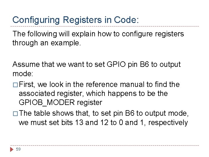
Configuring Registers in Code: The following will explain how to configure registers through an example. Assume that we want to set GPIO pin B 6 to output mode: � First, we look in the reference manual to find the associated register, which happens to be the GPIOB_MODER register � The table shows that, to set pin B 6 to output mode, we must set bits 13 and 12 to 0 and 1, respectively 59
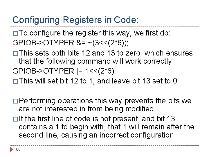
Configuring Registers in Code: � To configure the register this way, we first do: GPIOB->OTYPER &= ~(3<<(2*6)); � This sets both bits 12 and 13 to zero, which ensures that the following command will work correctly GPIOB->OTYPER |= 1<<(2*6); � This will set bit 12 to 1, and leave bit 13 set to 0 � Performing operations this way prevents the bits we are not interested in from being modified � If the first line of code is not present, and bit 13 contains a 1 to begin with, that 1 will remain after the second line, causing an incorrect configuration 60

Things to do before Lab 1: � Before � The True. Studio IDE will be used in all future labs � Also, please download the STEVAL project code � These 61 working on Lab 1, please install True. Studio resources can be found in the course Drive
- Slides: 61