Embedded Systems Design with Qsys and Altera Monitor
Embedded Systems Design with Qsys and Altera Monitor Program Tutorial #2
Embedded Systems Material for teaching embedded systems Tutorials on Altera’s embedded processors - Nios II - ARM Cortex A 9 Lab exercises that use these processors 2
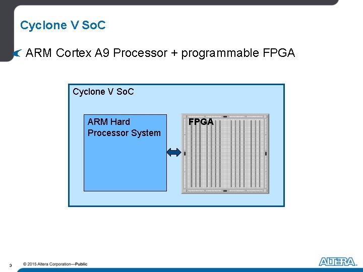
Cyclone V So. C ARM Cortex A 9 Processor + programmable FPGA Cyclone V So. C ARM Hard Processor System 3 FPGA
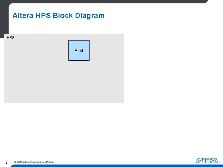
Altera HPS Block Diagram HPS ARM 4

Altera HPS Block Diagram 4 GB HPS ARM 3 GB L 2 Cache 2 GB 1 GB 0 GB 5
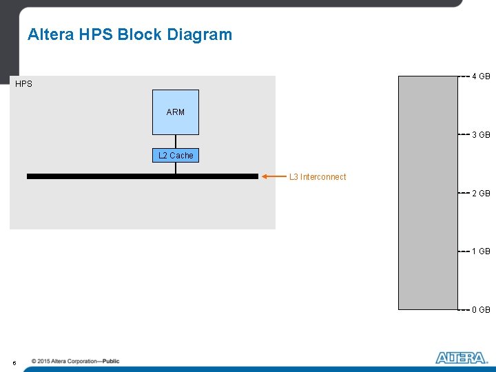
Altera HPS Block Diagram 4 GB HPS ARM 3 GB L 2 Cache L 3 Interconnect 2 GB 1 GB 0 GB 6
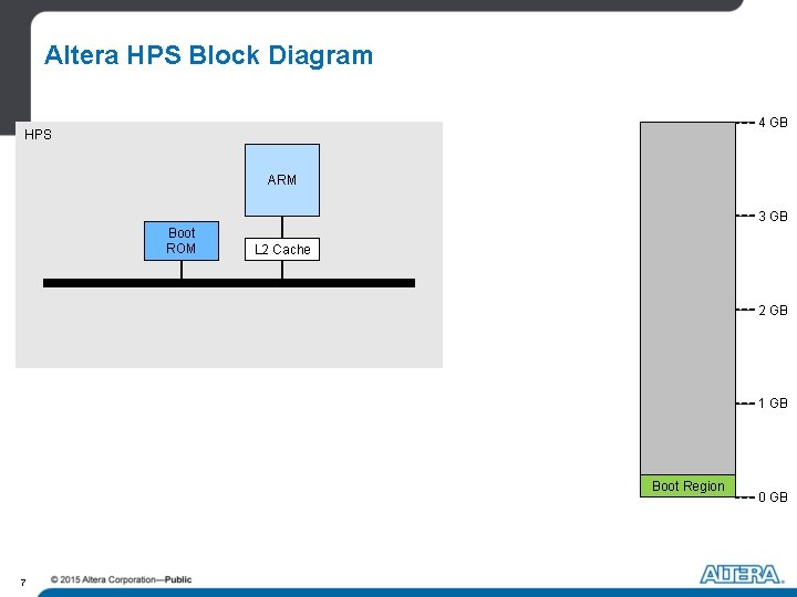
Altera HPS Block Diagram 4 GB HPS ARM 3 GB Boot ROM L 2 Cache 2 GB 1 GB Boot Region 7 0 GB
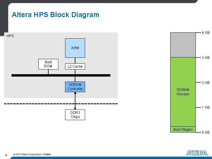
Altera HPS Block Diagram 4 GB HPS ARM 3 GB Boot ROM L 2 Cache SDRAM Controller 2 GB SDRAM Window 1 GB DDR 3 Chips Boot Region 8 0 GB
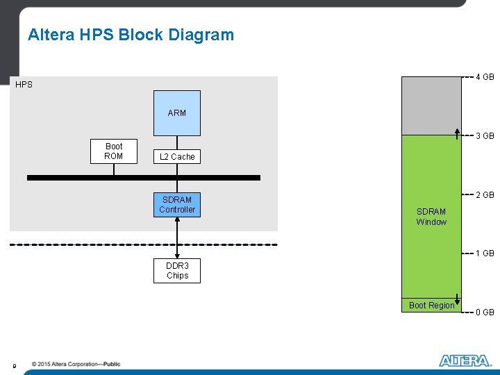
Altera HPS Block Diagram 4 GB HPS ARM 3 GB Boot ROM L 2 Cache SDRAM Controller 2 GB SDRAM Window 1 GB DDR 3 Chips Boot Region 9 0 GB
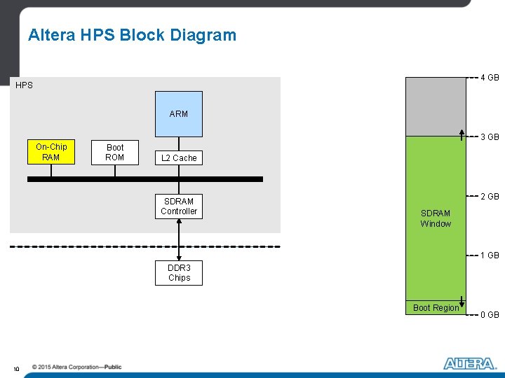
Altera HPS Block Diagram 4 GB HPS ARM 3 GB On-Chip RAM Boot ROM L 2 Cache SDRAM Controller 2 GB SDRAM Window 1 GB DDR 3 Chips Boot Region 10 0 GB
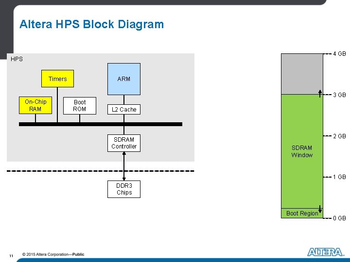
Altera HPS Block Diagram 4 GB HPS Timers ARM 3 GB On-Chip RAM Boot ROM L 2 Cache SDRAM Controller 2 GB SDRAM Window 1 GB DDR 3 Chips Boot Region 11 0 GB
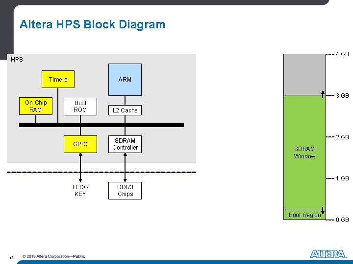
Altera HPS Block Diagram 4 GB HPS Timers ARM 3 GB On-Chip RAM Boot ROM GPIO L 2 Cache SDRAM Controller 2 GB SDRAM Window 1 GB LEDG KEY DDR 3 Chips Boot Region 12 0 GB
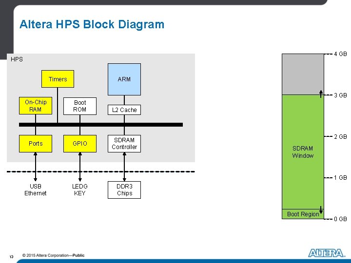
Altera HPS Block Diagram 4 GB HPS Timers ARM 3 GB On-Chip RAM Boot ROM Ports GPIO L 2 Cache SDRAM Controller 2 GB SDRAM Window 1 GB USB Ethernet LEDG KEY DDR 3 Chips Boot Region 13 0 GB
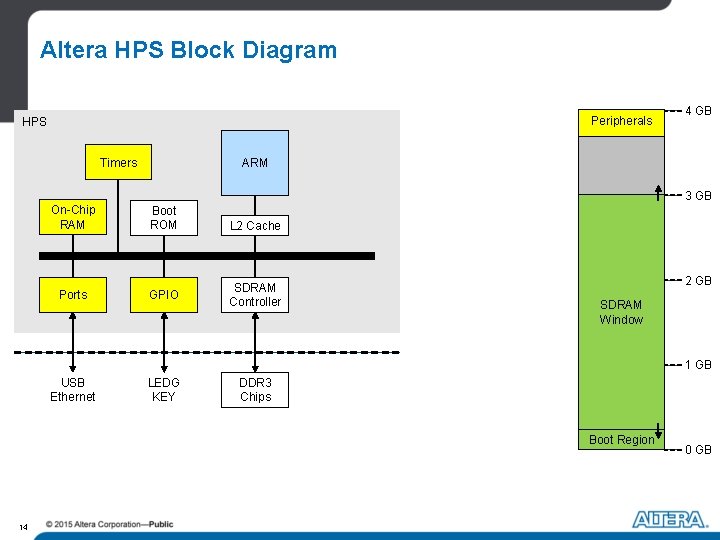
Altera HPS Block Diagram Peripherals HPS Timers 4 GB ARM 3 GB On-Chip RAM Boot ROM Ports GPIO L 2 Cache SDRAM Controller 2 GB SDRAM Window 1 GB USB Ethernet LEDG KEY DDR 3 Chips Boot Region 14 0 GB
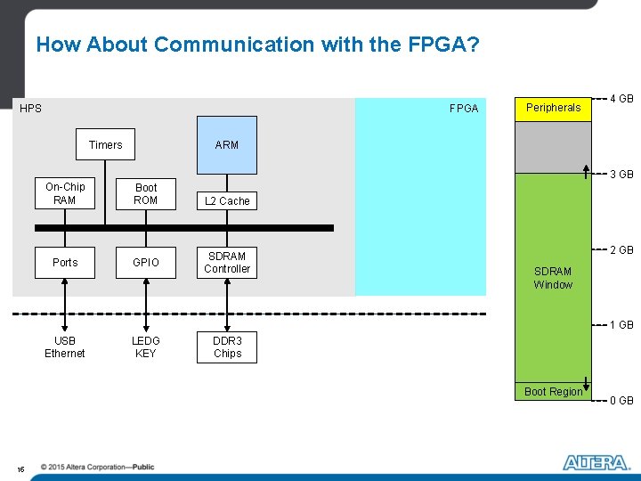
How About Communication with the FPGA? FPGA HPS Timers Peripherals 4 GB ARM 3 GB On-Chip RAM Boot ROM Ports GPIO L 2 Cache SDRAM Controller 2 GB SDRAM Window 1 GB USB Ethernet LEDG KEY DDR 3 Chips Boot Region 15 0 GB

There are Several Bridges Between the HPS and FPGA HPS Timers Peripherals 4 GB ARM 3 GB On-Chip RAM Boot ROM L 2 Cache Bridges Ports GPIO SDRAM Controller 2 GB SDRAM Window 1 GB USB Ethernet LEDG KEY DDR 3 Chips Boot Region 16 0 GB
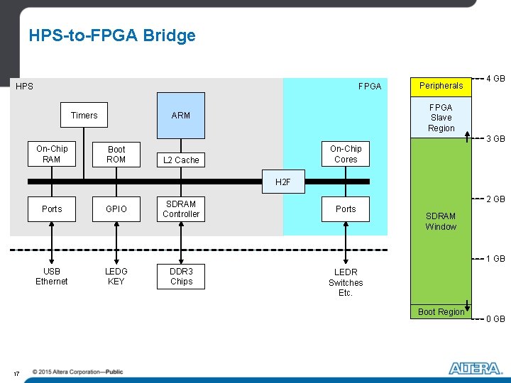
HPS-to-FPGA Bridge FPGA HPS Timers Peripherals 4 GB FPGA Slave Region ARM 3 GB On-Chip RAM Boot ROM On-Chip Cores L 2 Cache H 2 F Ports GPIO SDRAM Controller 2 GB Ports SDRAM Window 1 GB USB Ethernet LEDG KEY DDR 3 Chips LEDR Switches Etc. Boot Region 17 0 GB
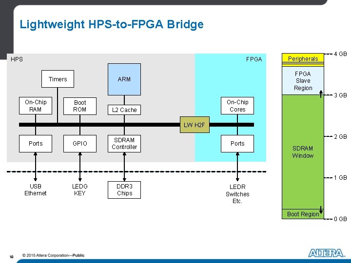
Lightweight HPS-to-FPGA Bridge FPGA HPS Timers Peripherals 4 GB FPGA Slave Region ARM 3 GB On-Chip RAM Boot ROM On-Chip Cores L 2 Cache LW H 2 F Ports GPIO SDRAM Controller 2 GB Ports SDRAM Window 1 GB USB Ethernet LEDG KEY DDR 3 Chips LEDR Switches Etc. Boot Region 18 0 GB
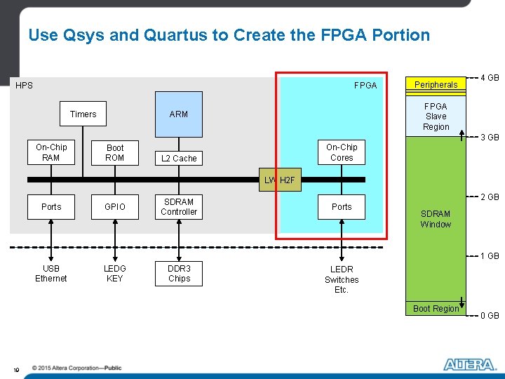
Use Qsys and Quartus to Create the FPGA Portion 1 HPS Timers FPGA Peripherals 4 GB FPGA Slave Region ARM 3 GB On-Chip RAM Boot ROM On-Chip Cores L 2 Cache LW H 2 F Ports GPIO SDRAM Controller 2 GB Ports SDRAM Window 1 GB USB Ethernet LEDG KEY DDR 3 Chips LEDR Switches Etc. Boot Region 19 0 GB
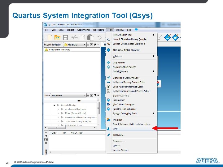
Quartus System Integration Tool (Qsys) 20
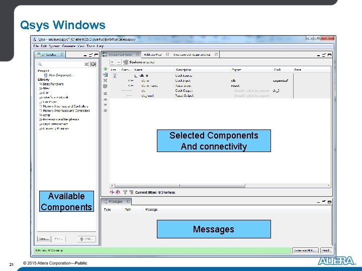
Qsys Windows Selected Components And connectivity Available Components Messages 21
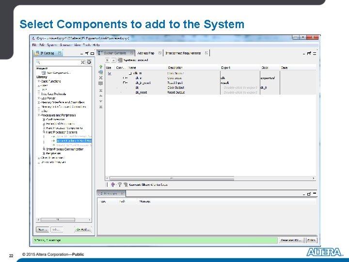
Select Components to add to the System 22
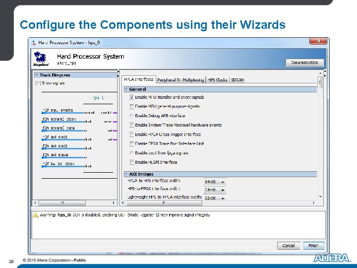
Configure the Components using their Wizards 23
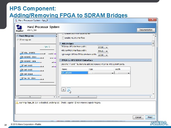
HPS Component: Adding/Removing FPGA to SDRAM Bridges 24
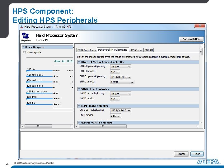
HPS Component: Editing HPS Peripherals 25
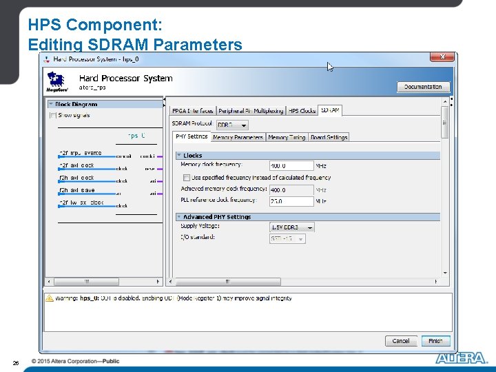
HPS Component: Editing SDRAM Parameters 26
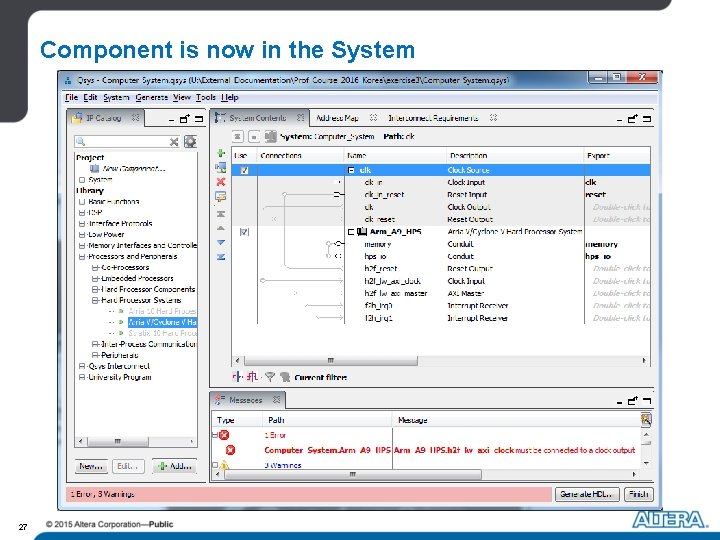
Component is now in the System 27
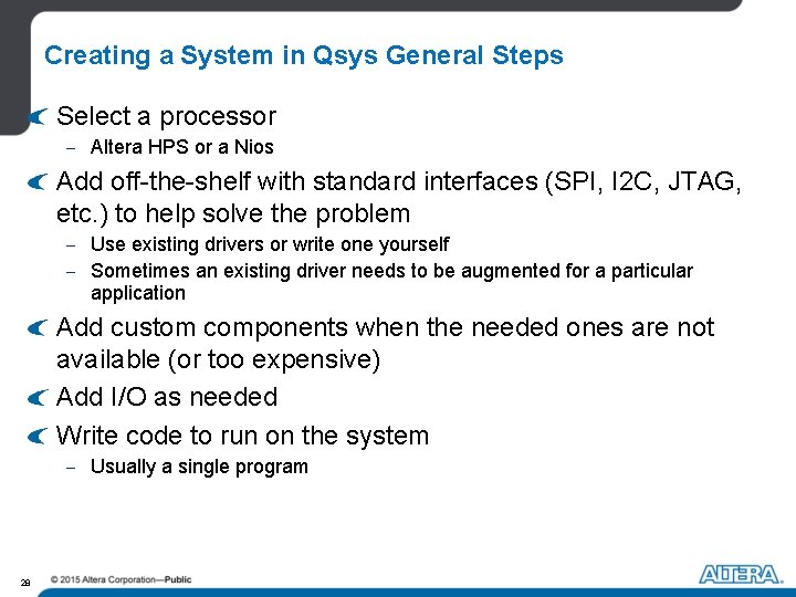
Creating a System in Qsys General Steps Select a processor - Altera HPS or a Nios Add off-the-shelf with standard interfaces (SPI, I 2 C, JTAG, etc. ) to help solve the problem - Use existing drivers or write one yourself - Sometimes an existing driver needs to be augmented for a particular application Add custom components when the needed ones are not available (or too expensive) Add I/O as needed Write code to run on the system - Usually a single program 28
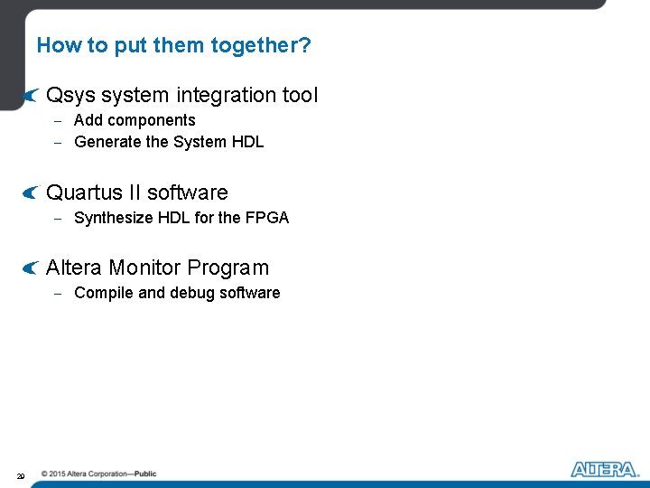
How to put them together? Qsys system integration tool - Add components - Generate the System HDL Quartus II software - Synthesize HDL for the FPGA Altera Monitor Program - Compile and debug software 29
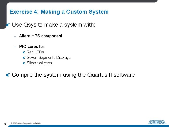
Exercise 4: Making a Custom System Use Qsys to make a system with: - Altera HPS component - PIO cores for: Red LEDs Seven Segments Displays Slider switches Compile the system using the Quartus II software 30
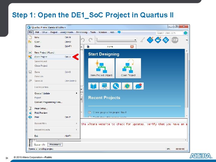
Step 1: Open the DE 1_So. C Project in Quartus II 31
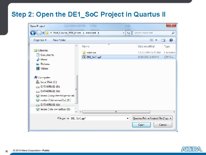
Step 2: Open the DE 1_So. C Project in Quartus II 32
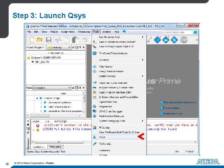
Step 3: Launch Qsys 33
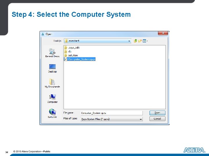
Step 4: Select the Computer System 34
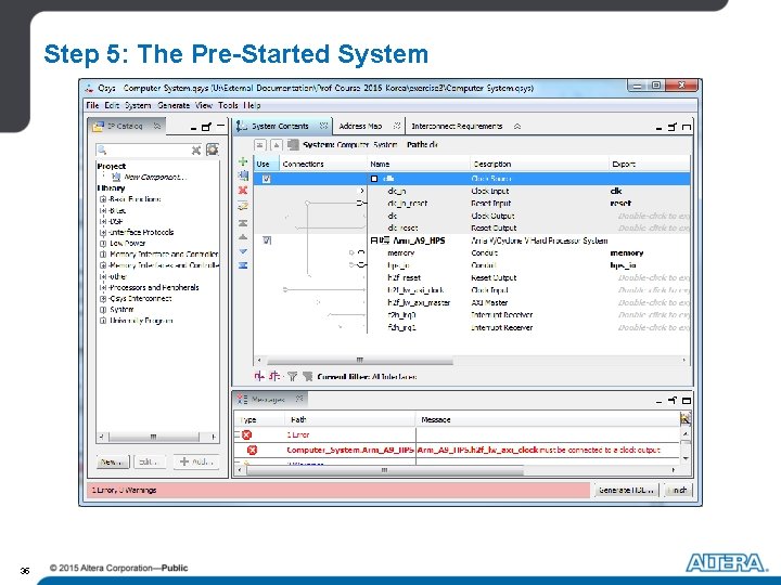
Step 5: The Pre-Started System 35
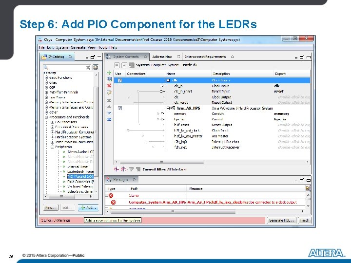
Step 6: Add PIO Component for the LEDRs 36

Step 7: Configure the PIO for the LEDRs 37
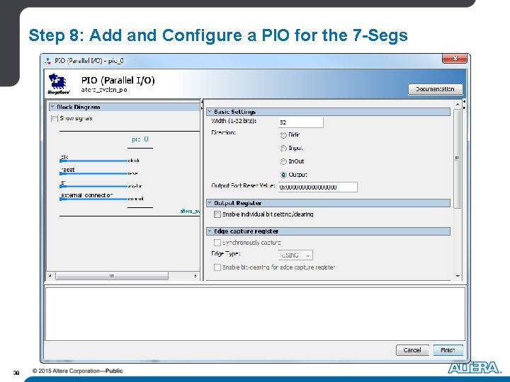
Step 8: Add and Configure a PIO for the 7 -Segs 38
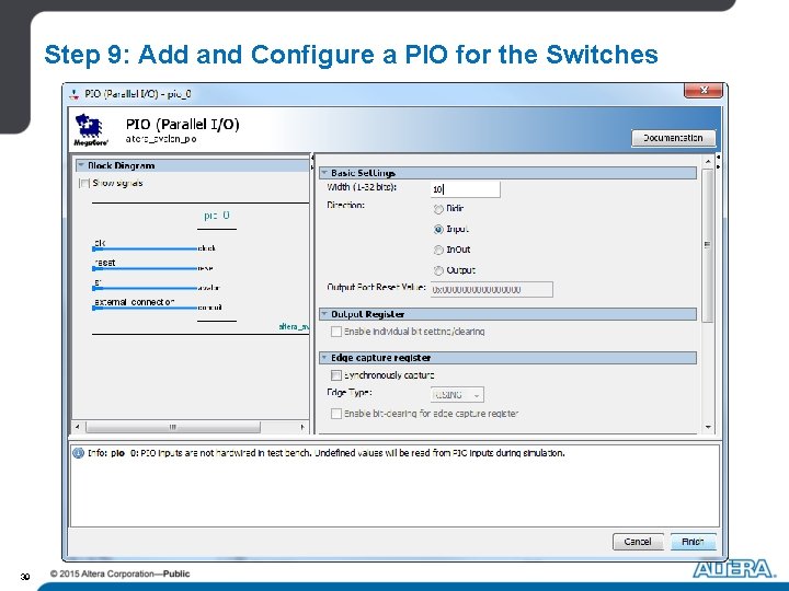
Step 9: Add and Configure a PIO for the Switches 39
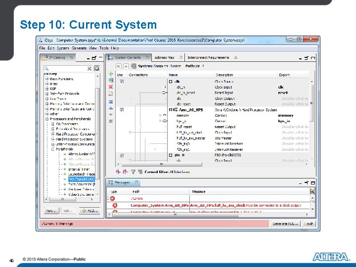
Step 10: Current System 40
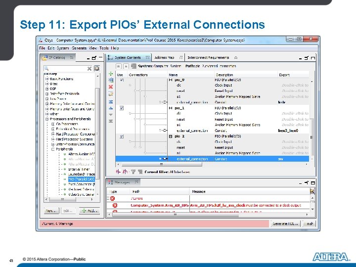
Step 11: Export PIOs’ External Connections 41
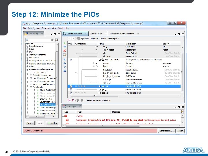
Step 12: Minimize the PIOs 42
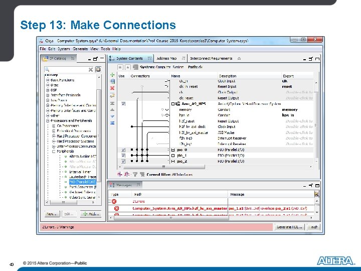
Step 13: Make Connections 43
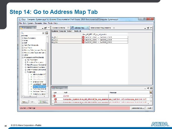
Step 14: Go to Address Map Tab 44
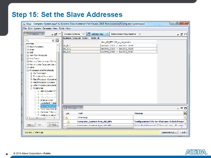
Step 15: Set the Slave Addresses 45
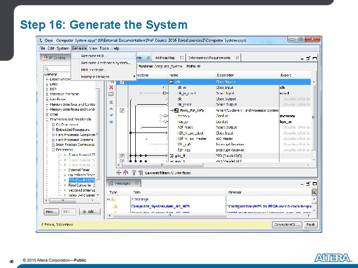
Step 16: Generate the System 46
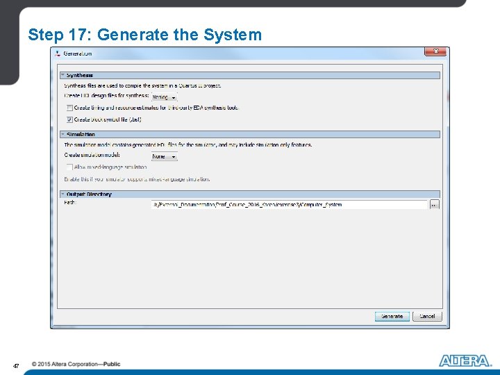
Step 17: Generate the System 47
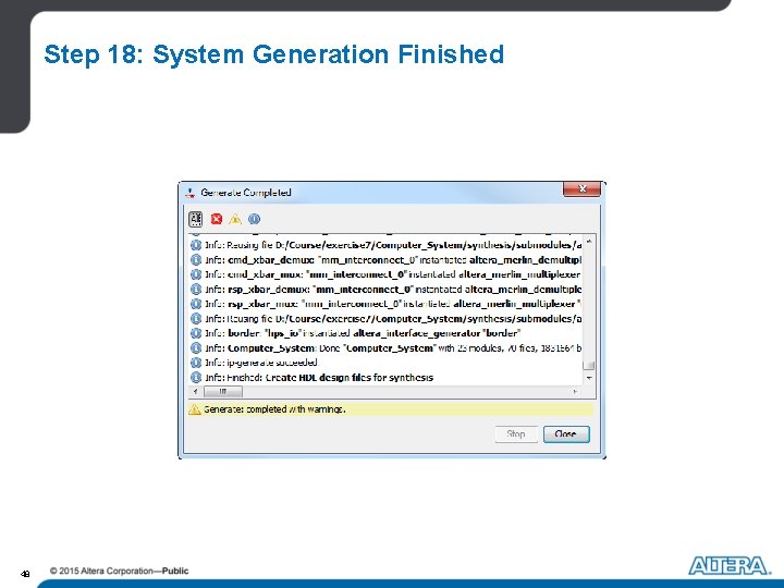
Step 18: System Generation Finished 48
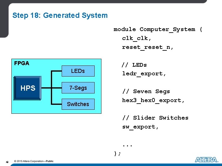
Step 18: Generated System module Computer_System ( clk_clk, reset_n, FPGA // LEDs ledr_export, LEDs HPS 7 -Segs // Seven Segs hex 3_hex 0_export, Switches // Slider Switches sw_export, . . . ); 49
Step 19: Create Top Level File for project System must be instantiated in your design - Must connect system ports to the I/O ports In this demo the top level file has been created for you - Compile your project. - Open the DE 1_So. C. v to examine the system connectivity while Quartus II compiles the project. 50
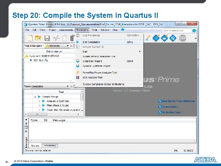
Step 20: Compile the System in Quartus II 51
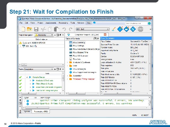
Step 21: Wait for Compilation to Finish 52
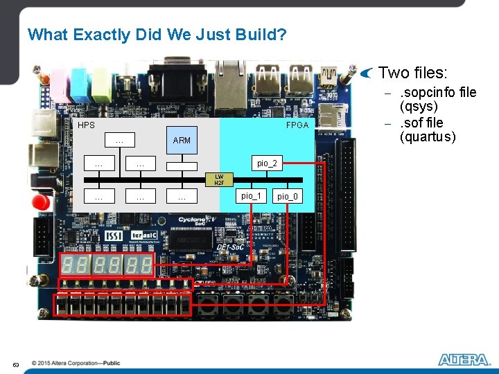
What Exactly Did We Just Build? Two files: -. sopcinfo file FPGA HPS … … … 53 ARM … … . … pio_2 LW H 2 F pio_1 pio_0 (qsys) -. sof file (quartus)
Hands-On Session Please read the instructions at - “/exercise 4/instructions. pdf” Use provided Quartus project “DE 1_So. C. qpf” Use pre-started Qsys system “”Computer_System. qsys” We will be walking around to help with any issues 54
Exercise 5: Developing an Embedded Application Write a software application to run on the system that we built in the previous exercise Compile the code using Altera Monitor Program Run the program and examine some debugging features of the Altera Monitor Program 55
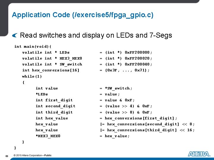
Application Code (/exercise 5/fpga_gpio. c) Read switches and display on LEDs and 7 -Segs int main(void)( volatile int * LEDs volatile int * HEX 3_HEX 0 volatile int * SW_switch int hex_conversions[16] while(1) { int value *LEDs int first_digit int second_digit int third_digit int hex_value *HEX 3_HEX 0 } } 56 = = (int *) 0 x. FF 200000; (int *) 0 x. FF 200020; (int *) 0 x. FF 200040; {0 x 3 F, . . . , 0 x 71}; = *SW_switch; = value & 0 x. F; = (value >> 4) & 0 x. F; = (value >> 8) & 0 x. F; = hex_conversions[first_digit]; |= hex_conversions[second_digit] << 8; |= hex_conversions[third_digit] << 16; = hex_value;
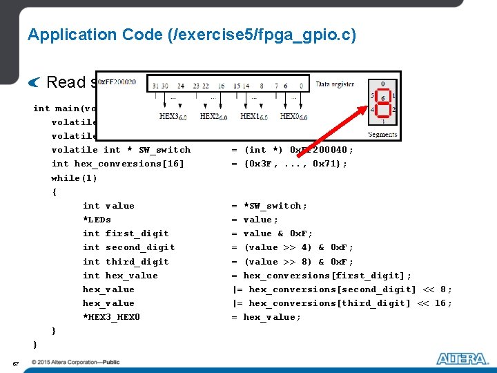
Application Code (/exercise 5/fpga_gpio. c) Read switches and display on LEDs and 7 -Segs int main(void)( volatile int * LEDs volatile int * HEX 3_HEX 0 volatile int * SW_switch int hex_conversions[16] while(1) { int value *LEDs int first_digit int second_digit int third_digit int hex_value *HEX 3_HEX 0 } } 57 = = (int *) 0 x. FF 200000; (int *) 0 x. FF 200020; (int *) 0 x. FF 200040; {0 x 3 F, . . . , 0 x 71}; = *SW_switch; = value & 0 x. F; = (value >> 4) & 0 x. F; = (value >> 8) & 0 x. F; = hex_conversions[first_digit]; |= hex_conversions[second_digit] << 8; |= hex_conversions[third_digit] << 16; = hex_value;

Application Code (/exercise 5/fpga_gpio. c) Read switches and display on LEDs and 7 -Segs int main(void)( volatile int * LEDs volatile int * HEX 3_HEX 0 volatile int * SW_switch int hex_conversions[16] while(1) { int value *LEDs int first_digit int second_digit int third_digit int hex_value *HEX 3_HEX 0 } } 58 = = (int *) 0 x. FF 200000; (int *) 0 x. FF 200020; (int *) 0 x. FF 200040; {0 x 3 F, . . . , 0 x 71}; = *SW_switch; = value & 0 x. F; = (value >> 4) & 0 x. F; = (value >> 8) & 0 x. F; = hex_conversions[first_digit]; |= hex_conversions[second_digit] << 8; |= hex_conversions[third_digit] << 16; = hex_value;
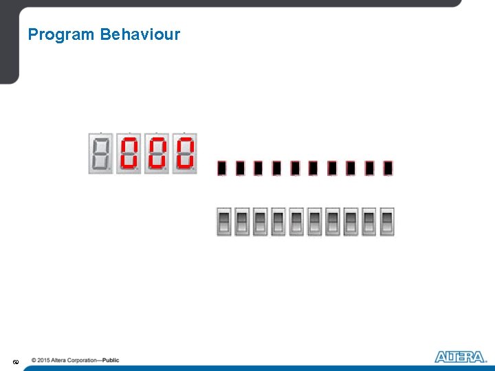
Program Behaviour 59
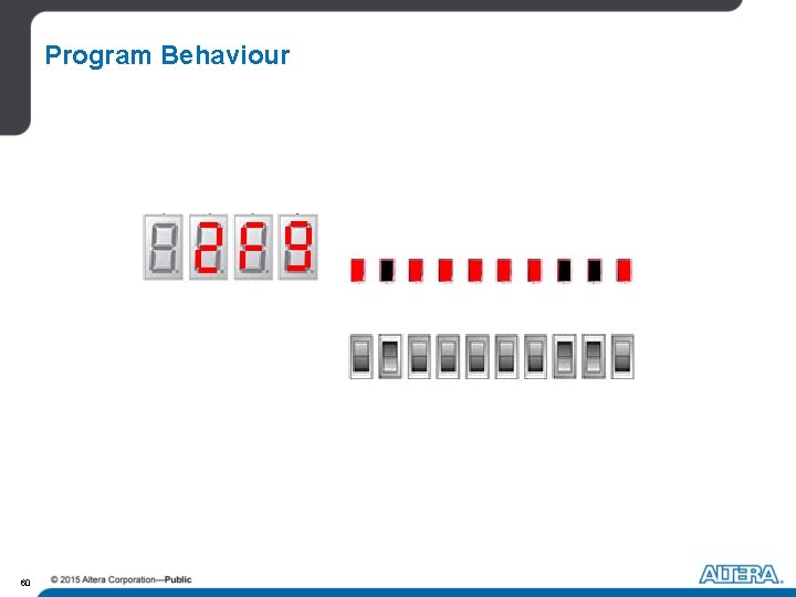
Program Behaviour 60
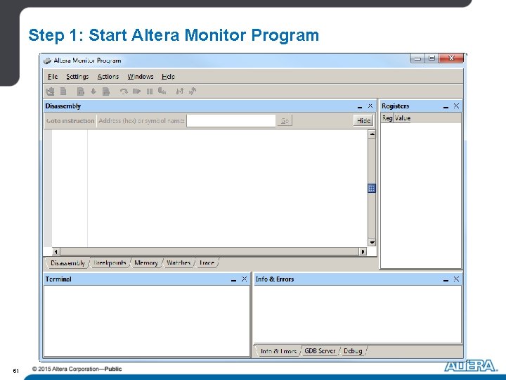
Step 1: Start Altera Monitor Program 61
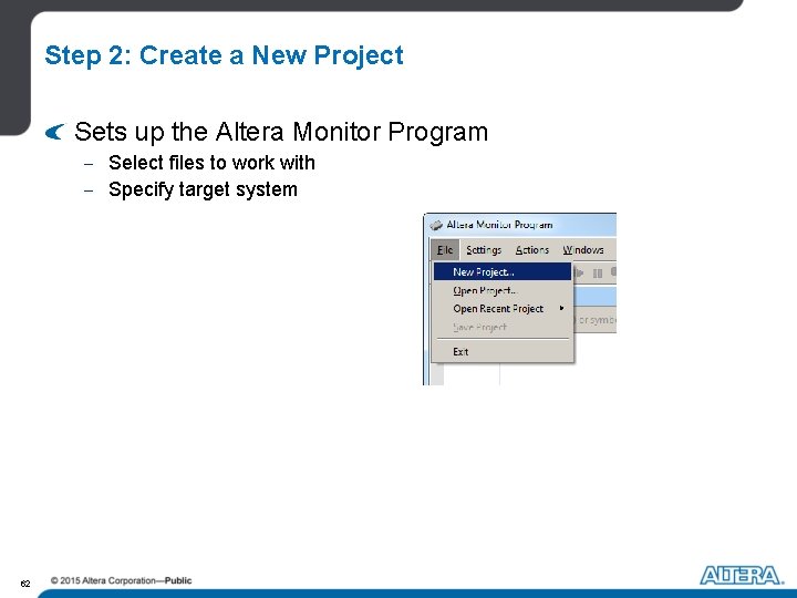
Step 2: Create a New Project Sets up the Altera Monitor Program - Select files to work with - Specify target system 62
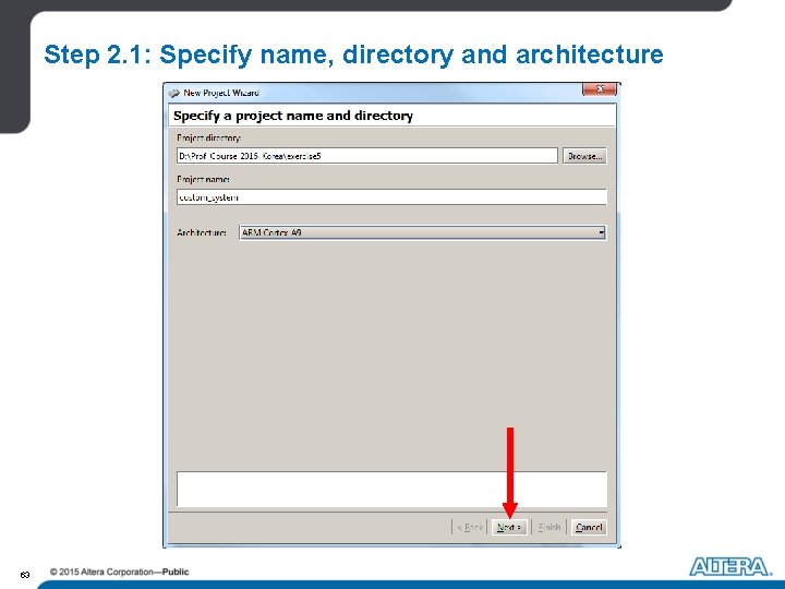
Step 2. 1: Specify name, directory and architecture 63
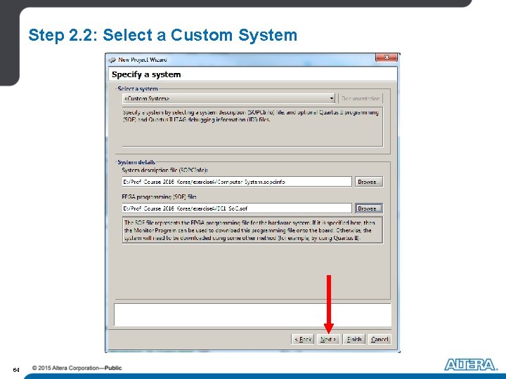
Step 2. 2: Select a Custom System 64
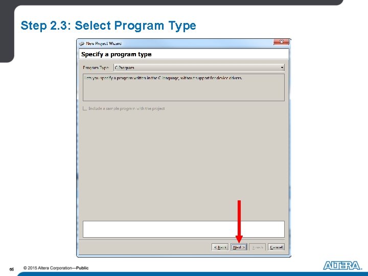
Step 2. 3: Select Program Type 65
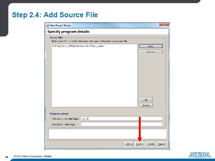
Step 2. 4: Add Source File 66
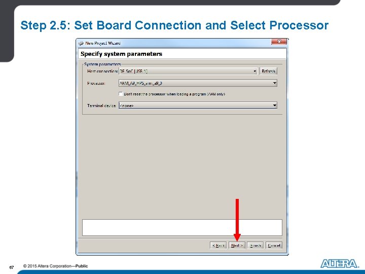
Step 2. 5: Set Board Connection and Select Processor 67
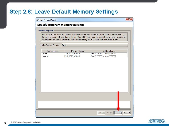
Step 2. 6: Leave Default Memory Settings 68
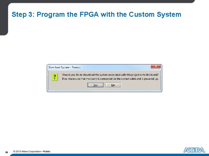
Step 3: Program the FPGA with the Custom System 69
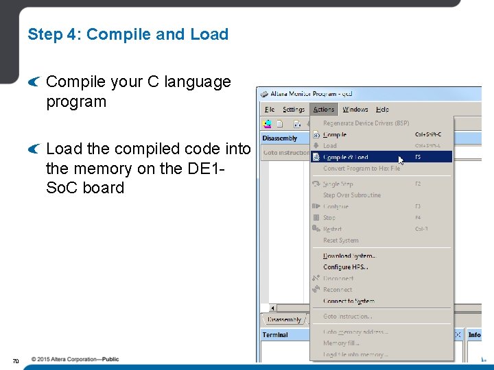
Step 4: Compile and Load Compile your C language program Load the compiled code into the memory on the DE 1 So. C board 70
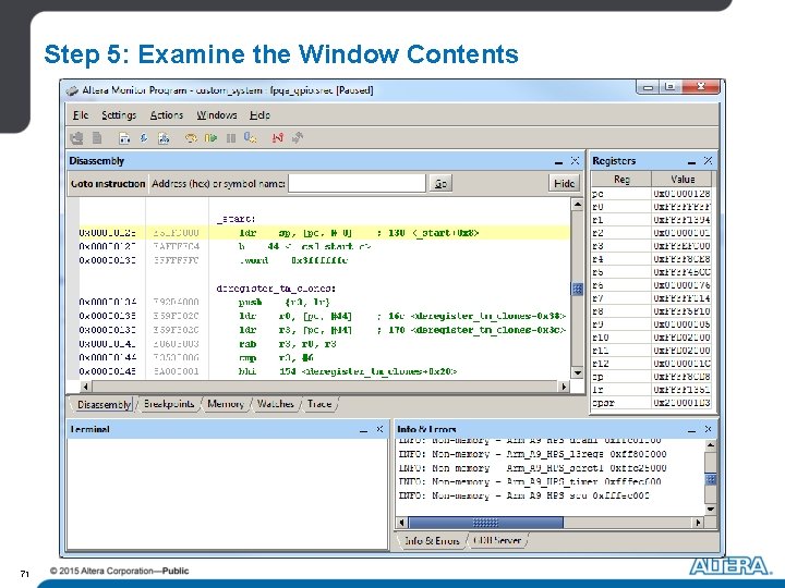
Step 5: Examine the Window Contents 71
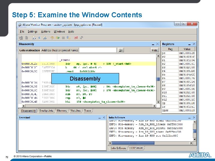
Step 5: Examine the Window Contents Disassembly 72
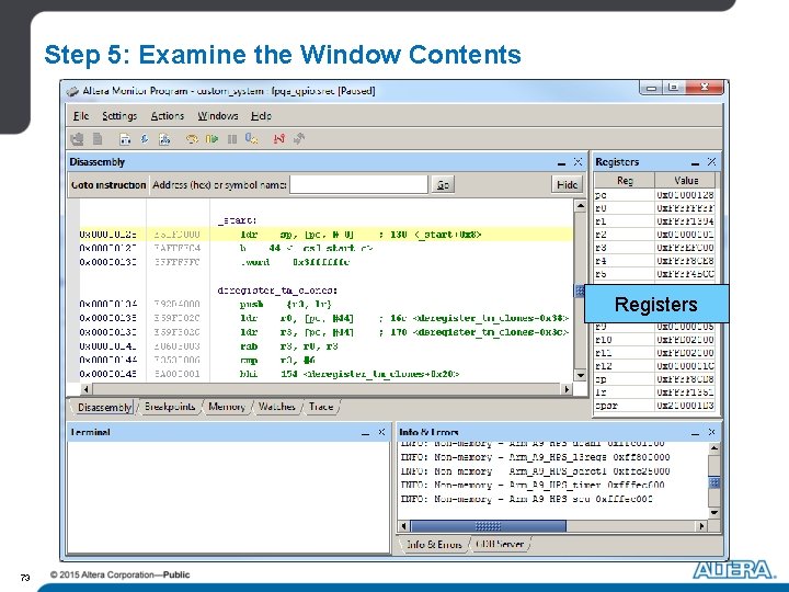
Step 5: Examine the Window Contents Registers 73
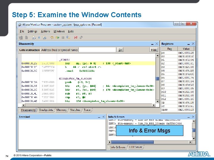
Step 5: Examine the Window Contents Info & Error Msgs 74
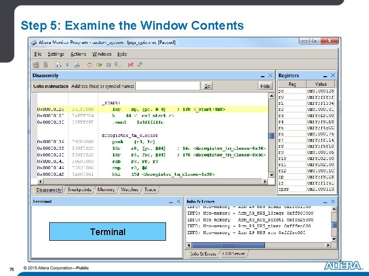
Step 5: Examine the Window Contents Terminal 75
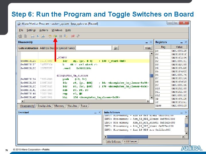
Step 6: Run the Program and Toggle Switches on Board 76
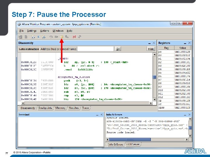
Step 7: Pause the Processor 77
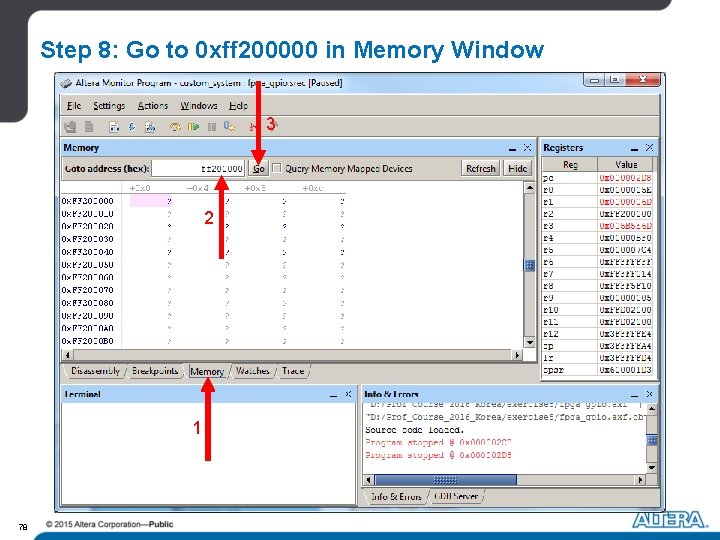
Step 8: Go to 0 xff 200000 in Memory Window 3 2 1 78
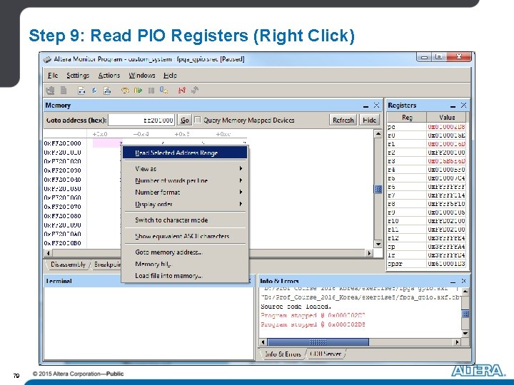
Step 9: Read PIO Registers (Right Click) 79
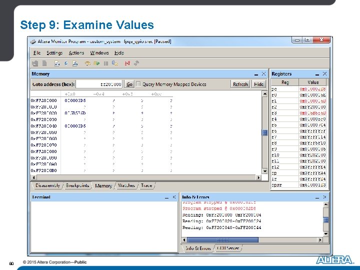
Step 9: Examine Values 80
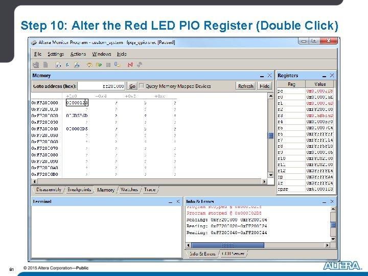
Step 10: Alter the Red LED PIO Register (Double Click) 81
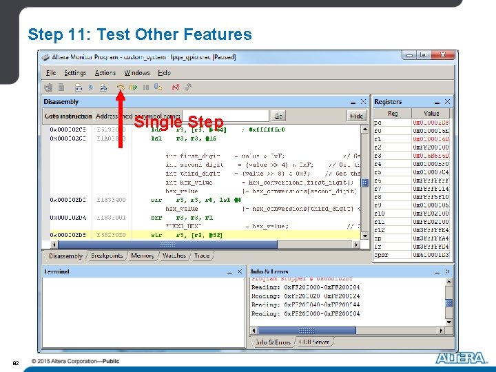
Step 11: Test Other Features Single Step 82
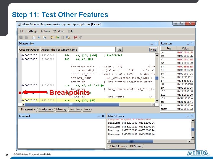
Step 11: Test Other Features Breakpoints 83
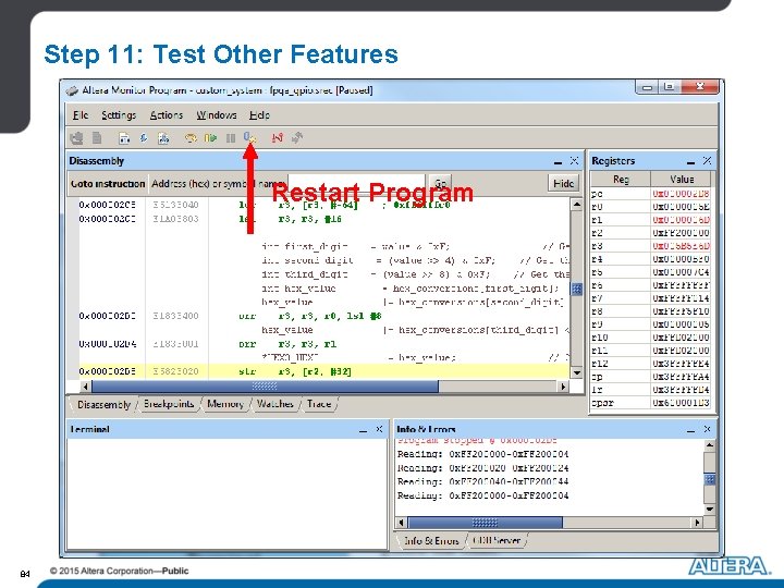
Step 11: Test Other Features Restart Program 84
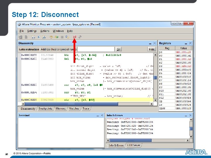
Step 12: Disconnect 85
Hands-On Session Please read the instructions at - “/exercise 5/instructions. pdf” If you did not finish exercise 4, use the solutions in /exercise 5/exercise 4_solutions/ We will be walking around to help with any issues 86
Summary of Tutorial #2 Learned how to - Use Qsys to build a system - Compile a Qsys system in Quartus - Write and compile applications for an ARM-based embedded system using Altera Monitor Program Where did we go from here? - Tutorials: Introduction to the Altera Qsys System Integration Tool Making Qsys Components Altera Monitor Program Tutorial for ARM - Embedded systems laboratory exercises - http: //university. altera. com 87
- Slides: 87