Embedded Systems A 3424 Unit V MEMORY MANAGEMENT

Embedded Systems (A 3424) Unit – V MEMORY MANAGEMENT Department of Electronics and Communication Engineering VARDHAMAN COLLEGE OF ENGINEERING Shamshabad, Hyderabad – 501218, India.
Embedded Systems (A 3424) Contents: CACHES Cache Architecture Cache Polices Flushing and Cleaning Caches Memory Management Unit (MMU) Details of the ARM MMU Page Tables Translation Lookaside Buffer Memory Access Permissions The Fast Context Switch Extension 2
Embedded Systems (A 3424) CACHES A cache is a small, fast array of memory placed between the processor core and main memory that stores portions of recently referenced main memory. The processor uses cache memory instead of main memory whenever possible to increase system performance. A cache is a write buffer—a very small first-in-first-out (FIFO) memory placed between the processor core and main memory. The main drawback is the difficulty of determining the execution time of a program. 3 Because data may or may not be present in cache at
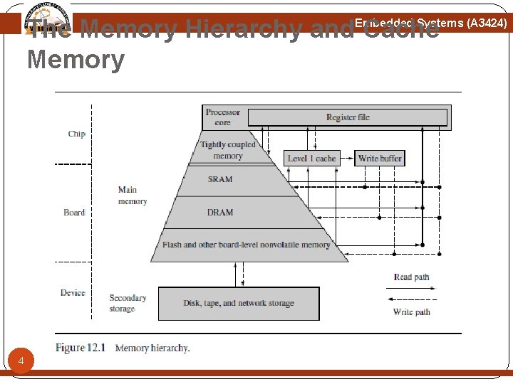
The Memory Hierarchy and Cache Memory Embedded Systems (A 3424) 4
The Memory Hierarchy and Cache Memory Embedded Systems (A 3424) The innermost level of the hierarchy is at the processor core. This memory is so tightly coupled to the processor that in many ways it is difficult to think of it as separate from the processor. This memory is known as a register file. These registers are integral to the processor core and provide the fastest possible memory access in the system. At the primary level, memory components are connected to the processor core through dedicated on-chip interfaces. It is at this level we find tightly coupled memory 5 (TCM) and level 1 cache.
The Memory Hierarchy and Cache Memory Embedded Systems (A 3424) The primary level is main memory. It includes volatile components like SRAM and DRAM, and nonvolatile components like flash memory. The purpose of main memory is to hold programs while they are running on a system. The next level is secondary storage—large, slow, relatively inexpensive mass storage devices such as disk drives or removable memory. Secondary memory is used to store unused portions of very large programs that do not fit in main memory and programs that are not currently executing. 6
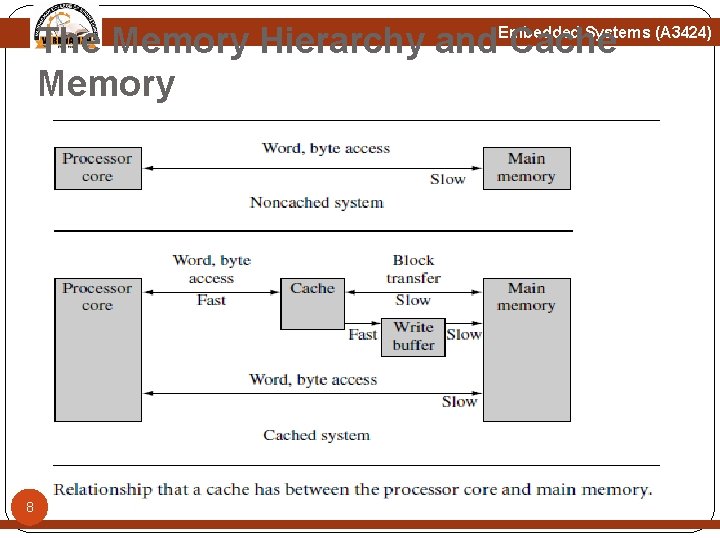
The Memory Hierarchy and Cache Memory Embedded Systems (A 3424) A memory hierarchy depends as much on architectural design as on the technology surrounding it. For example, TCM and SRAM are of the same technology yet differ in architectural placement: TCM is located on the chip, while SRAM is located on a board. In figure Level 1 (L 1) cache and write buffer. The L 1 cache is an array of high-speed, on-chip memory that temporarily holds code and data from a slower level. A cache holds this information to decrease the time required to access both instructions and data. The write buffer is a very small FIFO buffer that 7 supports writes to main memory from the cache.
The Memory Hierarchy and Cache Memory Embedded Systems (A 3424) 8
Embedded Systems (A 3424) Cache Architecture ARM uses two bus architectures in its cached cores, the Von Neumann and the Harvard. The Von Neumann and Harvard bus architectures differ in the separation of the instruction and data paths between the core and memory. A different cache design is used to support the two architectures. In processor cores using the Von Neumann architecture, there is a single cache used for instruction and data. This type of cache is known as a unified cache. In processor cores using the Harvard architecture, 9 there are two caches: an instruction cache (I-cache)
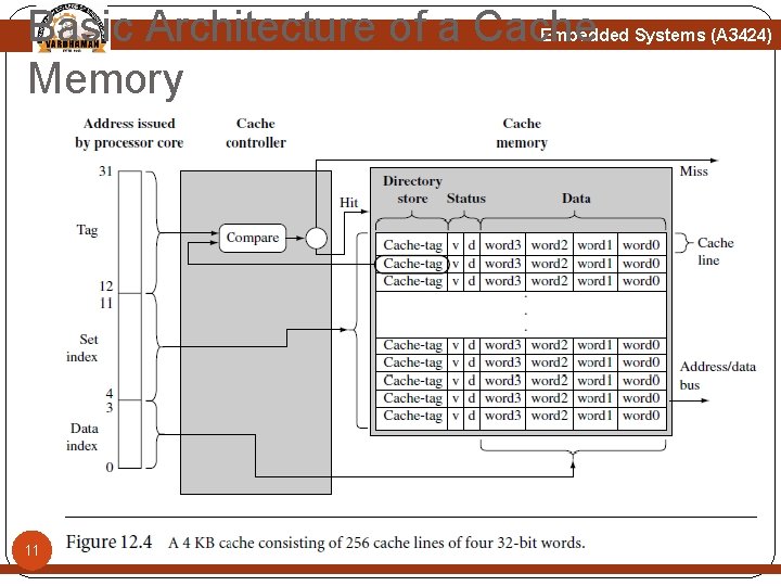
Embedded Systems (A 3424) Cache Architecture The two main elements of a cache are the cache controller and the cache memory. The cache memory is a dedicated memory array accessed in units called cache lines. The cache controller uses different portions of the address issued by the processor during a memory request to select parts of cache memory. 10
Basic Architecture of a Cache Memory Embedded Systems (A 3424) 11
Basic Architecture of a Cache Memory Embedded Systems (A 3424) A simple cache memory is shown above Figure. It has three main parts: A directory store, a data section, and status information. All three parts of the cache memory are present for each cache line. The cache must know where the information stored in a cache line originates from in main memory. It uses a directory store to hold the address identifying where the cache line was copied from main memory. 12 The directory entry is known as a cache-tag.
Basic Architecture of a Cache Memory Embedded Systems (A 3424) A cache memory must also store the data read from main memory. This information is held in the data section. There also status bits in cache memory to maintain state information. Two common status bits are the valid bit and dirty bit. A valid bit marks a cache line as active, meaning it contains live data originally taken from main memory and is currently available to the processor core on demand. A dirty bit defines whether or not a cache line contains data that is different from the value it 13 represents in main memory.
Basic Operation of a Cache Controller Embedded Systems (A 3424) The cache controller is hardware that copies code or data from main memory to cache memory automatically. It processes a request by dividing the address of the request into three fields, the tag field, the set index field, and the data index field. First, the controller uses the set index portion of the address to locate the cache line within the cache memory that might hold the requested code or data. The controller then checks the valid bit to determine if the cache line is active, and compares the cache-tag to the tag field of the requested address. If both the status check and comparison succeed, it is a 14 cache hit.
Basic Operation of a Cache Controller Embedded Systems (A 3424) On a cache miss, the controller copies an entire cache line from main memory to cache memory and provides the requested code or data to the processor. The copying of a cache from main memory to cache memory is known as a cache line fill. On a cache hit, the controller supplies the code or data directly from cache memory to the processor. To do this it moves to the next step, which is to use the data index field of the address request to select the actual code or data in the cache line and provide it to the processor. 15
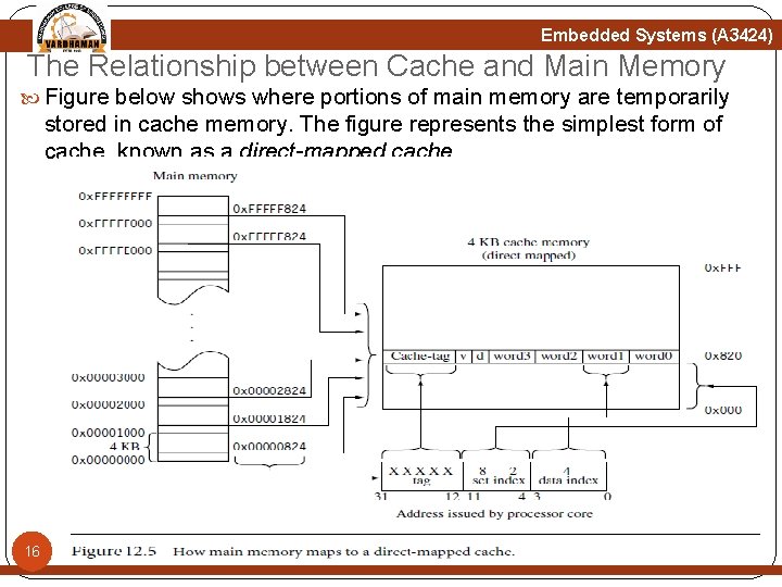
Embedded Systems (A 3424) The Relationship between Cache and Main Memory Figure below shows where portions of main memory are temporarily stored in cache memory. The figure represents the simplest form of cache, known as a direct-mapped cache. 16
Embedded Systems (A 3424) The Relationship between Cache and Main Memory In a direct-mapped cache each addressed location in main memory maps to a single location in cache memory. Since main memory is much larger than cache memory, there are many addresses in main memory that map to the same single location in cache memory. The figure shows this relationship for the class of addresses ending in 0 x 824. The set index selects the one location in cache where all values in memory with an ending address of 0 x 824 are stored. The data index selects the word/halfword/byte in the cache line, in this case the second word in the cache line. The tag field is the portion of the address that is compared to the cache-tag value found in the directory store. During a cache line fill the cache controller may forward the loading data to the core at the same time it is copying it to cache; 17 this is known as data streaming.
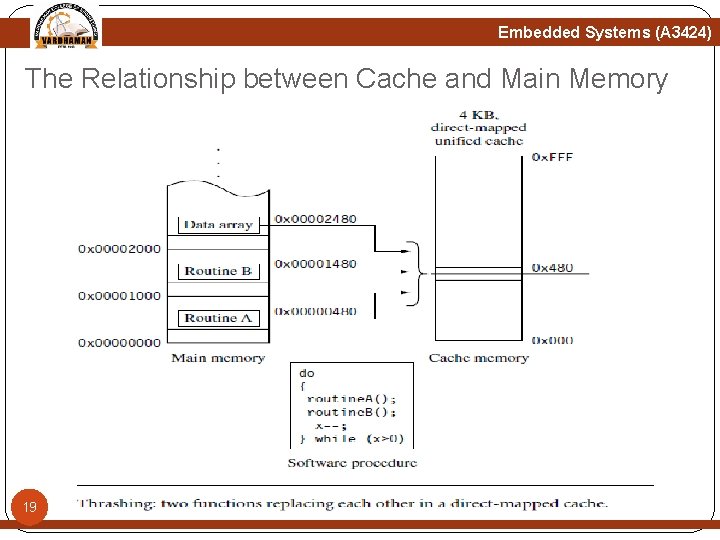
Embedded Systems (A 3424) The Relationship between Cache and Main Memory If valid data exists in this cache line but represents another address block in main memory, the entire cache line is evicted and replaced by the cache line containing the requested address. This process of removing an existing cache line as part of servicing a cache miss is known as eviction—returning the contents of a cache line to main memory from the cache to make room for new data that needs to be loaded in cache. A direct-mapped cache is a simple solution, but there is a design cost inherent in having a single location available to store a value from main memory. Direct-mapped caches are subject to high levels of thrashing—a software battle for the same location in cache memory. The result of thrashing is the repeated loading and eviction of a cache line. 18 Figure 12. 6 takes Figure 12. 5 and overlays a simple, contrived
Embedded Systems (A 3424) The Relationship between Cache and Main Memory 19
Embedded Systems (A 3424) The Relationship between Cache and Main Memory The procedure calls two routines repeatedly in a do while loop. Each routine has the same set index address; that is, the routines are found at addresses in physical memory that map to the same location in cache memory. The first time through the loop, routine A is placed in the cache as it executes. When the procedure calls routine B, it evicts routine A a cache line at a time as it is loaded into cache and executed. On the second time through the loop, routine A replaces routine B, and then routine B replaces routine A. Repeated cache misses result in continuous eviction of the routine that not running. This is cache thrashing. 20
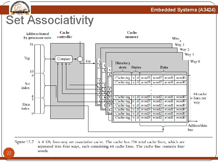
Embedded Systems (A 3424) Set Associativity Some caches include an additional design feature to 21 reduce the frequency of thrashing. This structural design feature is a change that divides the cache memory into smaller equal units, called ways. Figure below is still a four KB cache; however, the set index now addresses more than one cache line— it points to one cache line in each way. Instead of one way of 256 lines, the cache has four ways of 64 lines. The four cache lines with the same set index are said to be in the same set, which is the origin of the name “set index. ”
Embedded Systems (A 3424) Set Associativity 22
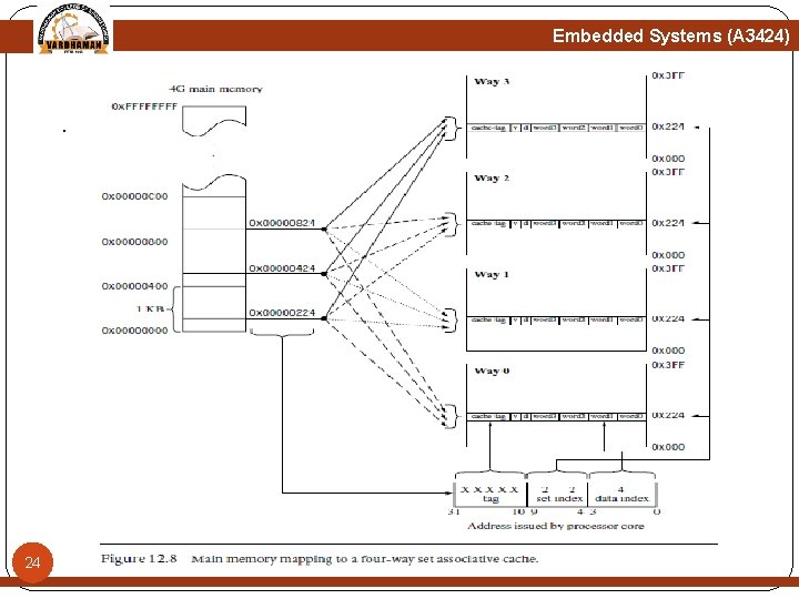
Embedded Systems (A 3424) Set Associativity A data or code block from main memory can be allocated to any of the four ways in a set Two sequential blocks from main memory can be stored as cache lines in the same way or two different ways. The important thing to note is that the data or code blocks from a specific location in main memory can be stored in any cache line that is a member of a set. The placement of values within a set is exclusive to prevent the same code or data block from simultaneously occupying two cache lines in a set. The mapping of main memory to a cache changes in a fourway set associative cache. Figure 12. 8 shows the differences. Any single location in main memory now maps to four different locations in the cache. 23
Embedded Systems (A 3424) . 24
Embedded Systems (A 3424) Set Associativity Any single location in main memory now maps to four different locations in the cache. The bit field for the tag is now two bits larger, and the set index bit field is two bits smaller. The size of the area of main memory that maps to cache is now 1 KB instead of 4 KB. This means that the likelihood of mapping cache line data blocks to the same set is now four times higher. 25
Embedded Systems (A 3424) Increasing Set Associativity As the associativity of a cache controller goes up, the probability of thrashing goes down. The ideal goal would be to maximize the set associativity of a cache by designing it so any main memory location maps to any cache line. A cache that does this is known as a fully associative cache. As the associativity increases, so does the complexity of the hardware that supports it. One method used by hardware designers to increase the set associativity of a cache includes a content addressable memory (CAM). A CAM uses a set of comparators to compare the input tag address with a cache-tag stored in each valid cache line. Using a CAM allows many more cache-tags to be compared simultaneously, thereby increasing the number of cache lines that can be included in a set. 26
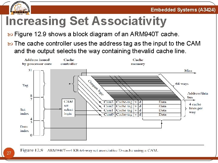
Embedded Systems (A 3424) Increasing Set Associativity Figure 12. 9 shows a block diagram of an ARM 940 T cache. The cache controller uses the address tag as the input to the CAM and the output selects the way containing thevalid cache line. 27
Embedded Systems (A 3424) Increasing Set Associativity The tag portion of the requested address is used as an input to the four CAMs that simultaneously compare the input tag with all cache-tags stored in the 64 ways. If there is a match, cache data is provided by the cache memory. If no match occurs, a miss signal is generated by the memory controller. The controller enables one of four CAMs using the set index bits. The indexed CAM then selects a cache line in cache memory and the data index portion of the core address selects the requested word, halfword, or byte within the cache line. 28
Write Buffers Embedded Systems (A 3424) A write buffer is a very small, fast FIFO memory buffer that temporarily holds data that the processor would normally write to main memory. In a system without a write buffer, the processor writes directly to main memory. In a system with a write buffer, data is written at high speed to the FIFO and then emptied to slower main memory. The write buffer reduces the processor time taken to write small blocks of sequential data to main memory. The FIFO memory of the write buffer is at the same level in the memory hierarchy as the L 1 cache. Data written to the write buffer is not available for reading until it has exited the write buffer to main memory. The same holds true for an evicted cache line: it too cannot be read while it is in the write buffer. 29 This is one of the reasons that the FIFO depth of a write buffer is
Embedded Systems (A 3424) Write Buffers Some write buffers are not strictly FIFO buffers. The ARM 10 family, for example, supports coalescing —the merging of write operations into a single cache line. The write buffer will merge the new value into an existing cache line in the write buffer if they represent the same data block in main memory. Coalescing is also known as write merging, write collapsing, or write combining. 30
Embedded Systems (A 3424) Measuring Cache Efficiency There are two terms used to characterize the cache efficiency of a program: The cache hit rate The cache miss rate The hit rate is the number of cache hits divided by the total number of memory requests over a given time interval. The value is expressed as a percentage: Hitrate = ( cache hits/memory requests) x 100; The miss rate is similar in form: the total cache misses divided by the total number of memory requests expressed as a percentage over a time interval. The miss rate also equals 100 minus the hit rate. Two other terms used in cache performance measurement are The hit time—the time it takes to access a memory location in the cache 31 The miss penalty—the time it takes to load a cache line from main memory into cache.
Embedded Systems (A 3424) Cache Policy There are three policies that determine the operation of a cache: The write policy The replacement policy The allocation policy The cache write policy determines where data is stored during processor write operations. The replacement policy selects the cache line in a set that is used for the next line fill during a cache miss. The allocation policy determines when the cache controller allocates a cache line. Write Policy—Writeback or Writethrough When the processor core writes to memory, the cache controller has two alternatives for its write policy. The controller can write to both the cache and main memory, updating the values in both locations; this approach is known as 32 writethrough.
Embedded Systems (A 3424) Cache Policy Writethrough: When the cache controller uses a writethrough policy, it writes to both cache and main memory when there is a cache hit on write, ensuring that the cache and main memor stay coherent at all times. Because of the write to main memory, a writethrough policy is slower than a writeback policy. Writeback: When a cache controller uses a writeback policy, it writes to valid cache data memory and not to main memory. Caches configured as writeback caches must use one or more of the dirty bits in the cache line status information block. When a cache controller in writeback writes a value to cache memory, it sets the dirty bit true. 33
Embedded Systems (A 3424) Cache Policy Cache Line Replacement Policies On a cache miss, the cache controller must select a cache line from the available set in cache memory to store the new information from main memory. The cache line selected for replacement is known as a victim. The process of selecting and replacing a victim cache line is known as eviction. The strategy implemented in a cache controller to select the next victim is called its replacement policy. ARM cached cores support two replacement policies, either pseudorandom or round-robin. 34
Embedded Systems (A 3424) Cache Policy Cache Line Replacement Policies Round-robin or cyclic replacement simply selects the next cache line in a set to replace. The selection algorithm uses a sequential, incrementing victim counter that increments each time the cache controller allocates a cache line. When the victim counter reaches a maximum value, it is reset to a defined base value. Pseudorandom replacement randomly selects the next cache line in a set to replace. The selection algorithm uses a nonsequential incrementing victim counter. When the victim counter reaches a maximum value, it is reset to 35 a defined base value.
Embedded Systems (A 3424) Cache Policy Allocation Policy on a Cache Miss There are two strategies ARM caches may use to allocate a cache line after a the occurrence of a cache miss. The first strategy is known as read-allocate, and the second strategy is known as read-write-allocate. A read allocate on cache miss policy allocates a cache line only during a read from main memory. If the victim cache line contains valid data, then it is written to main memory before the cache line is filled with new data. A read-write allocate on cache miss policy allocates a cache line for either a read or write to memory. Any load or store operation made to main memory, which is not in cache memory, allocates a cache line. 36
Flushing and Cleaning Cache Memory Embedded Systems (A 3424) ARM uses the terms flush and clean to describe two basic operations performed on a cache. To “flush a cache” is to clear it of any stored data. Flushing simply clears the valid bit in the affected cache line. The term invalidate is sometimes used in place of the term flush. To “clean a cache” is to force a write of dirty cache lines from the cache out to main memory and clear the dirty bits in the cache line. Cleaning a cache reestablishes coherence between cached memory and main memory. 37
- Slides: 37