Elimination of the Crossover Distortion of Class AB

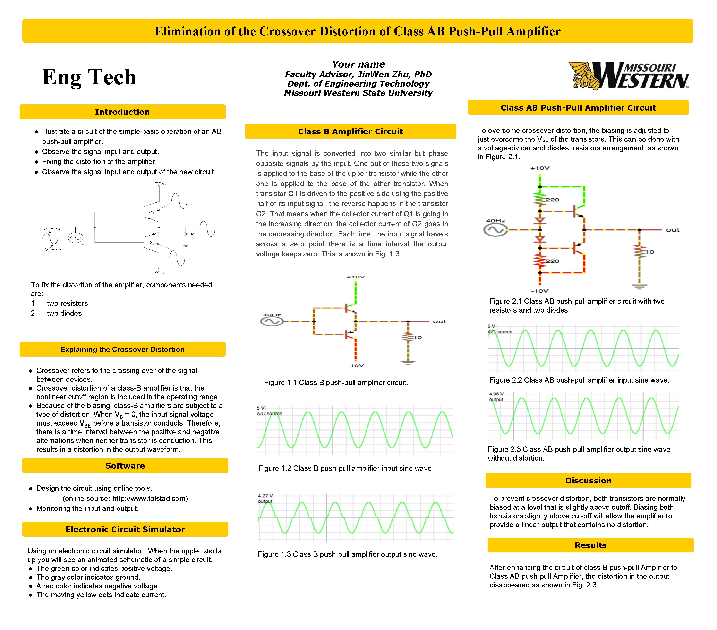
Elimination of the Crossover Distortion of Class AB Push-Pull Amplifier Eng Tech Your name Faculty Advisor, Jin. Wen Zhu, Ph. D Dept. of Engineering Technology Missouri Western State University Class AB Push-Pull Amplifier Circuit Introduction ● Illustrate a circuit of the simple basic operation of an AB push-pull amplifier. ● Observe the signal input and output. ● Fixing the distortion of the amplifier. ● Observe the signal input and output of the new circuit. Class B Amplifier Circuit The input signal is converted into two similar but phase opposite signals by the input. One out of these two signals is applied to the base of the upper transistor while the other one is applied to the base of the other transistor. When transistor Q 1 is driven to the positive side using the positive half of its input signal, the reverse happens in the transistor Q 2. That means when the collector current of Q 1 is going in the increasing direction, the collector current of Q 2 goes in the decreasing direction. Each time, the input signal travels across a zero point there is a time interval the output voltage keeps zero. This is shown in Fig. 1. 3. To fix the distortion of the amplifier, components needed are: 1. two resistors. 2. two diodes. To overcome crossover distortion, the biasing is adjusted to just overcome the VBE of the transistors. This can be done with a voltage-divider and diodes, resistors arrangement, as shown in Figure 2. 1 Class AB push-pull amplifier circuit with two resistors and two diodes. Explaining the Crossover Distortion ● Crossover refers to the crossing over of the signal between devices. ● Crossover distortion of a class-B amplifier is that the nonlinear cutoff region is included in the operating range. ● Because of the biasing, class-B amplifiers are subject to a type of distortion. When VB = 0, the input signal voltage must exceed VBE before a transistor conducts. Therefore, there is a time interval between the positive and negative alternations when neither transistor is conduction. This results in a distortion in the output waveform. Software Figure 1. 1 Class B push-pull amplifier circuit. Figure 2. 3 Class AB push-pull amplifier output sine wave without distortion. Figure 1. 2 Class B push-pull amplifier input sine wave. Discussion ● Design the circuit using online tools. (online source: http: //www. falstad. com) ● Monitoring the input and output. To prevent crossover distortion, both transistors are normally biased at a level that is slightly above cutoff. Biasing both transistors slightly above cut-off will allow the amplifier to provide a linear output that contains no distortion. Electronic Circuit Simulator Using an electronic circuit simulator. When the applet starts up you will see an animated schematic of a simple circuit. ● The green color indicates positive voltage. ● The gray color indicates ground. ● A red color indicates negative voltage. ● The moving yellow dots indicate current. Figure 2. 2 Class AB push-pull amplifier input sine wave. Results Figure 1. 3 Class B push-pull amplifier output sine wave. After enhancing the circuit of class B push-pull Amplifier to Class AB push-pull Amplifier, the distortion in the output disappeared as shown in Fig. 2. 3.
- Slides: 1