Electrostatic Discharge ESD TIPL 1401 TI Precision Labs
Electrostatic Discharge (ESD) TIPL 1401 TI Precision Labs – Op Amps Presented by Marek Lis
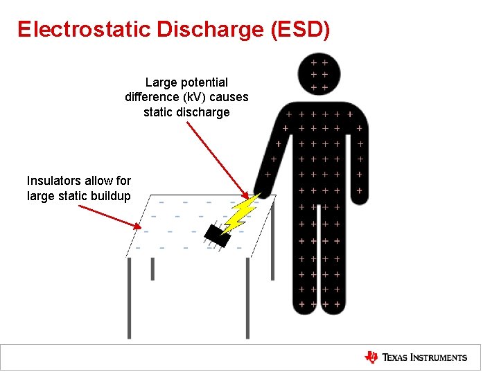
Electrostatic Discharge (ESD) Large potential difference (k. V) causes static discharge Insulators allow for large static buildup
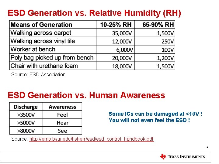
ESD Generation vs. Relative Humidity (RH) Source: ESD Association ESD Generation vs. Human Awareness Some ICs can be damaged at <10 V ! You will not even feel the ESD ! Source: http: //emp. byui. edu/fisherr/esd_control_handbook. pdf 3
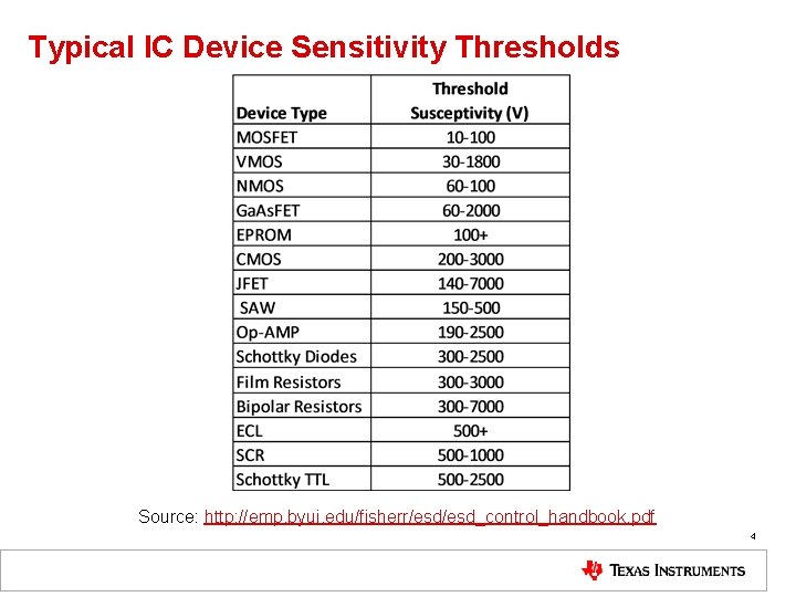
Typical IC Device Sensitivity Thresholds Source: http: //emp. byui. edu/fisherr/esd_control_handbook. pdf 4
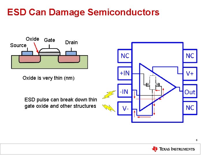
ESD Can Damage Semiconductors Oxide Gate Source Drain Oxide is very thin (nm) ESD pulse can break down thin gate oxide and other structures 5
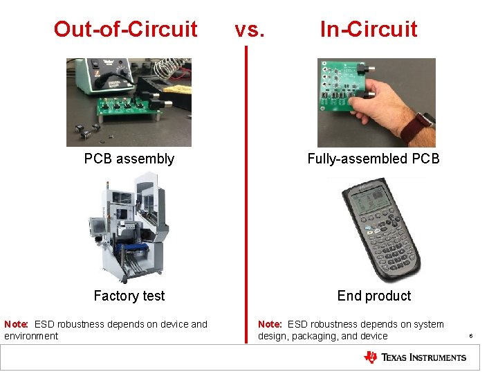
Out-of-Circuit vs. In-Circuit PCB assembly Fully-assembled PCB Factory test End product Note: ESD robustness depends on device and environment Note: ESD robustness depends on system design, packaging, and device 6
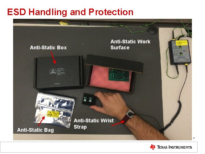
ESD Handling and Protection Anti-Static Box Anti-Static Bag Anti-Static Work Surface Anti-Static Wrist Strap 7
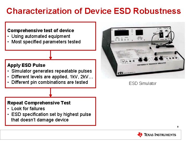
Characterization of Device ESD Robustness Comprehensive test of device • Using automated equipment • Most specified parameters tested Apply ESD Pulse • Simulator generates repeatable pulses • Different levels are applied, 1 k. V, 2 k. V… • Different pin combinations are tested ESD Simulator Repeat Comprehensive Test • Look for failures • ESD specification set by highest pulse that doesn’t damage device 8
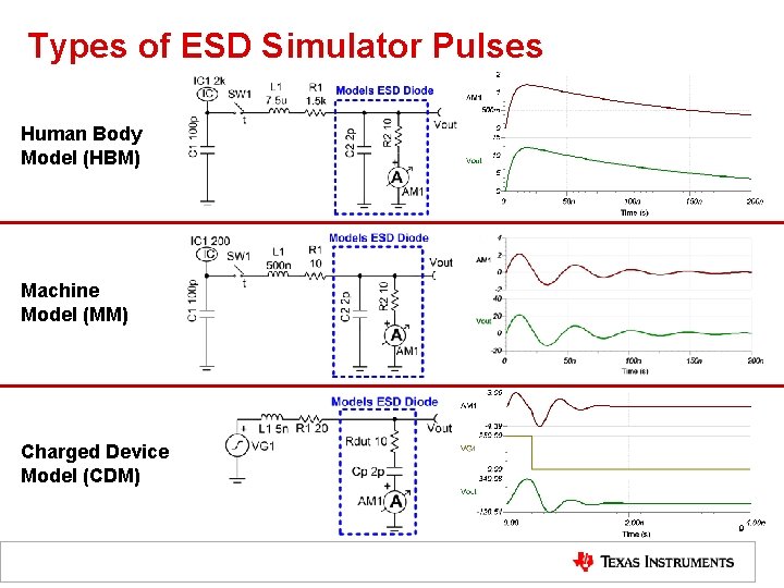
Types of ESD Simulator Pulses Human Body Model (HBM) Machine Model (MM) Charged Device Model (CDM) 9
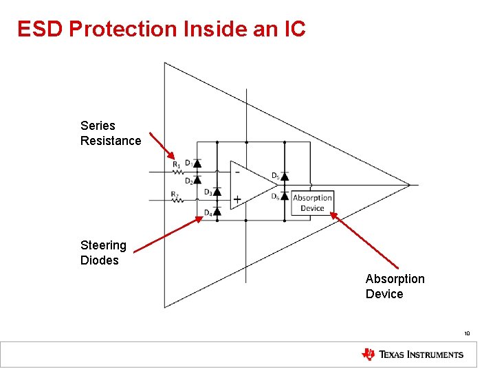
ESD Protection Inside an IC Series Resistance Steering Diodes Absorption Device 10
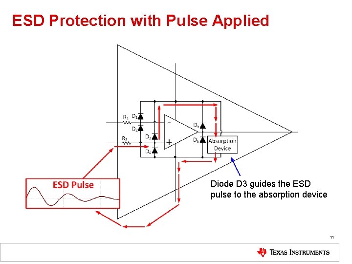
ESD Protection with Pulse Applied Diode D 3 guides the ESD pulse to the absorption device 11
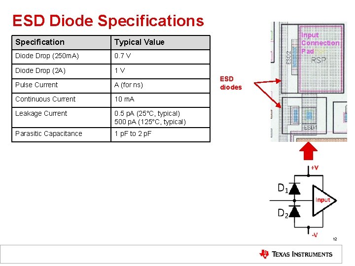
ESD Diode Specifications Specification Typical Value Diode Drop (250 m. A) 0. 7 V Diode Drop (2 A) 1 V Pulse Current A (for ns) Continuous Current 10 m. A Leakage Current 0. 5 p. A (25°C, typical) 500 p. A (125°C, typical) Parasitic Capacitance 1 p. F to 2 p. F Input Connection Pad ESD diodes 12
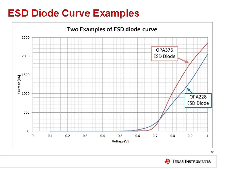
ESD Diode Curve Examples 13
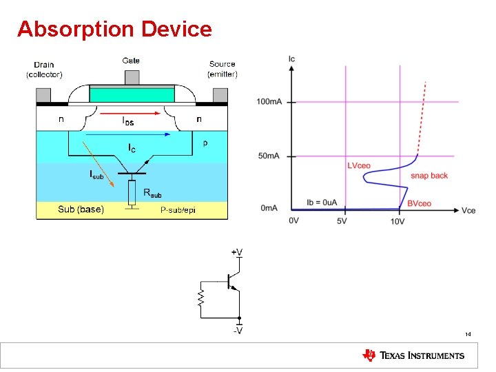
Absorption Device 14
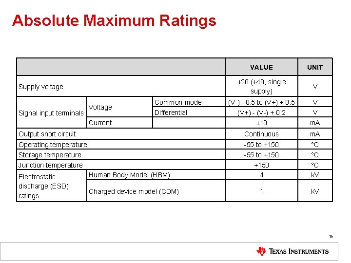
Absolute Maximum Ratings VALUE UNIT ± 20 (+40, single supply) V (V-) - 0. 5 to (V+) + 0. 5 (V+) - (V-) + 0. 2 V V ± 10 m. A Output short circuit Continuous m. A Operating temperature Storage temperature Junction temperature -55 to +150 4 °C °C °C k. V 1 k. V Supply voltage Signal input terminals Voltage Common-mode Differential Current Electrostatic discharge (ESD) ratings Human Body Model (HBM) Charged device model (CDM) 15
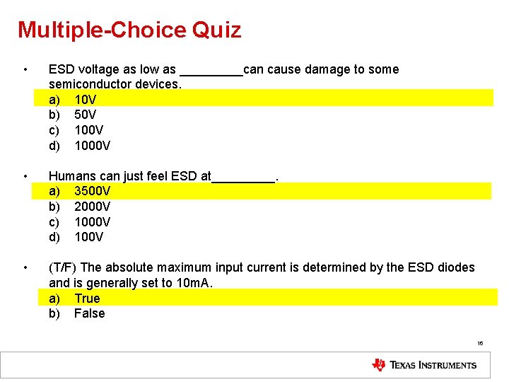
Multiple-Choice Quiz • ESD voltage as low as _____can cause damage to some semiconductor devices. a) 10 V b) 50 V c) 100 V d) 1000 V • Humans can just feel ESD at_____. a) 3500 V b) 2000 V c) 1000 V d) 100 V • (T/F) The absolute maximum input current is determined by the ESD diodes and is generally set to 10 m. A. a) True b) False 16
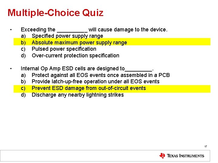
Multiple-Choice Quiz • Exceeding the _____ will cause damage to the device. a) Specified power supply range b) Absolute maximum power supply range c) Pulsed power specification d) Over-current protection specification • Internal Op Amp ESD cells are designed to_____. a) Protect against all EOS events once assembled in a PCB b) Provide latch-up-free operation under all EOS events c) Prevent ESD damage from out-of-circuit events d) Discharge any nearby lightning strikes 17
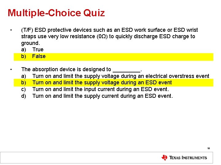
Multiple-Choice Quiz • (T/F) ESD protective devices such as an ESD work surface or ESD wrist straps use very low resistance (0Ω) to quickly discharge ESD charge to ground. a) True b) False • The absorption device is designed to _____. a) Turn on and limit the supply voltage during an electrical overstress event b) Turn on and limit the supply voltage during an ESD event c) Turn on and limit the input current during an ESD event. d) Turn on and limit the supply current during an ESD event. 18
Electrical Overstress – 1 TIPL 1411 TI Precision Labs – Op Amps Presented by Marek Lis
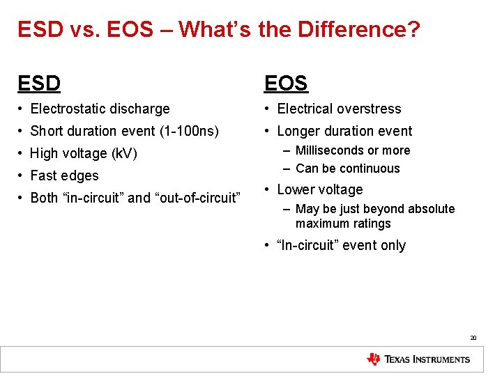
ESD vs. EOS – What’s the Difference? ESD EOS • Electrostatic discharge • Electrical overstress • Short duration event (1 -100 ns) • Longer duration event • High voltage (k. V) • Fast edges • Both “in-circuit” and “out-of-circuit” – Milliseconds or more – Can be continuous • Lower voltage – May be just beyond absolute maximum ratings • “In-circuit” event only 20
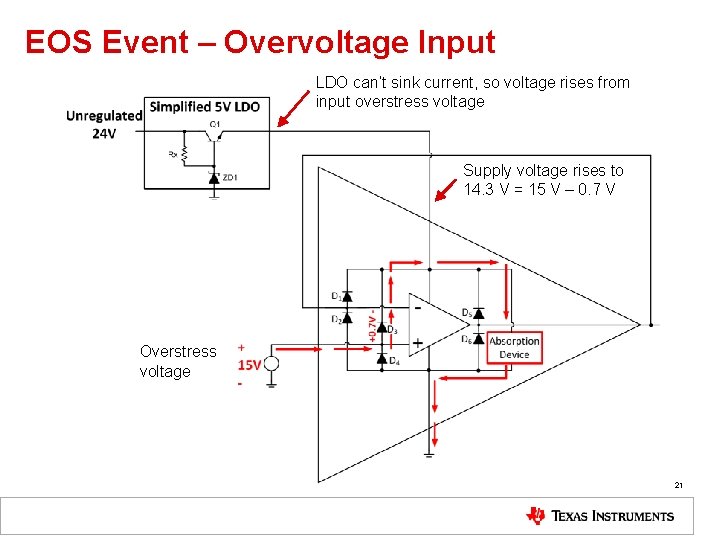
EOS Event – Overvoltage Input LDO can’t sink current, so voltage rises from input overstress voltage Supply voltage rises to 14. 3 V = 15 V – 0. 7 V Overstress voltage 21
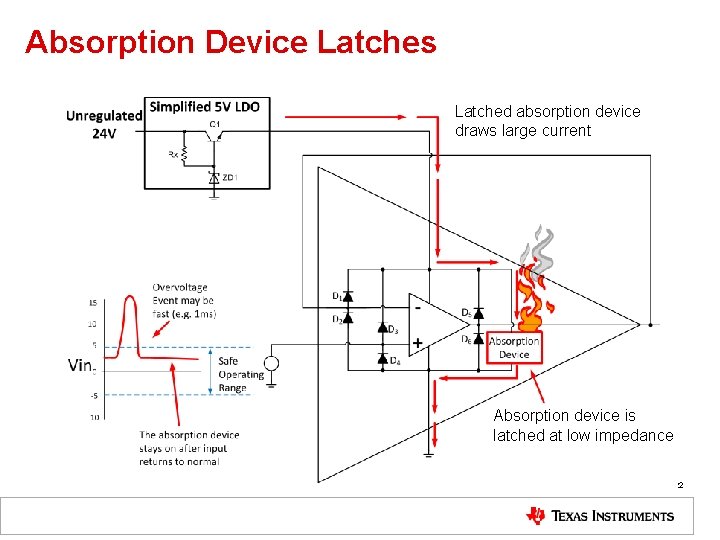
Absorption Device Latches Latched absorption device draws large current Absorption device is latched at low impedance 22
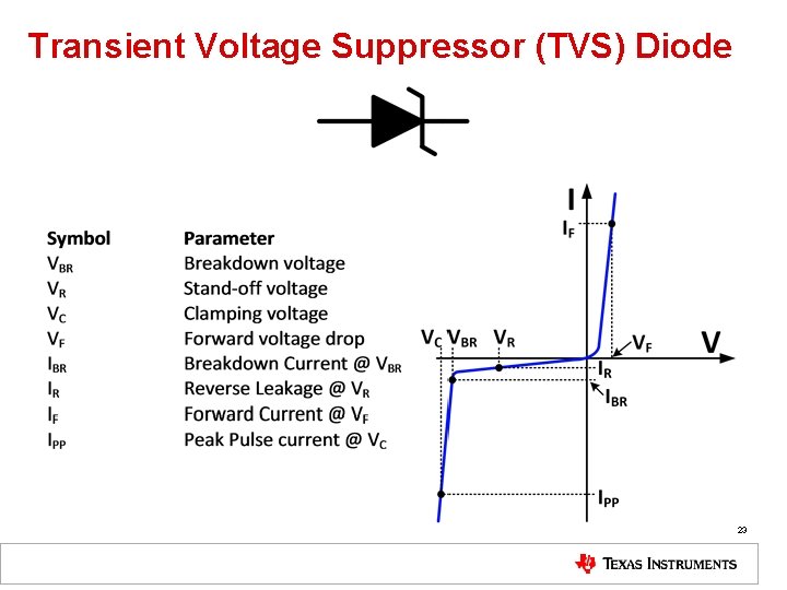
Transient Voltage Suppressor (TVS) Diode 23
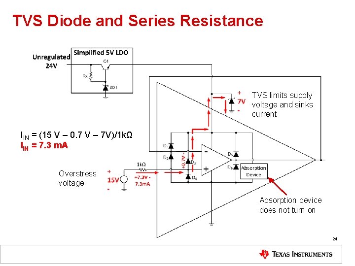
TVS Diode and Series Resistance TVS limits supply voltage and sinks current IIN = (15 V – 0. 7 V – 7 V)/1 kΩ IIN = 7. 3 m. A Overstress voltage Absorption device does not turn on 24
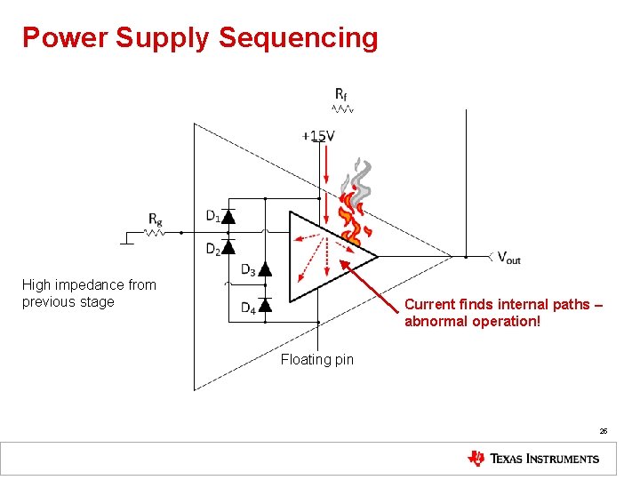
Power Supply Sequencing High impedance from previous stage Current finds internal paths – abnormal operation! Floating pin 25
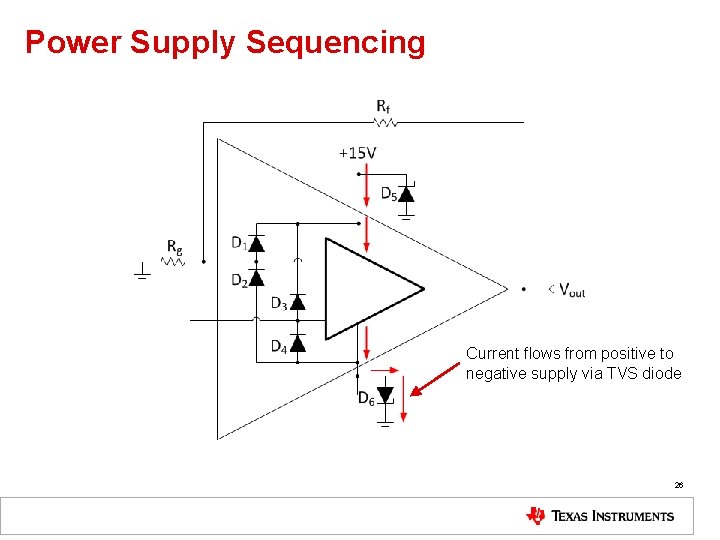
Power Supply Sequencing Current flows from positive to negative supply via TVS diode 26
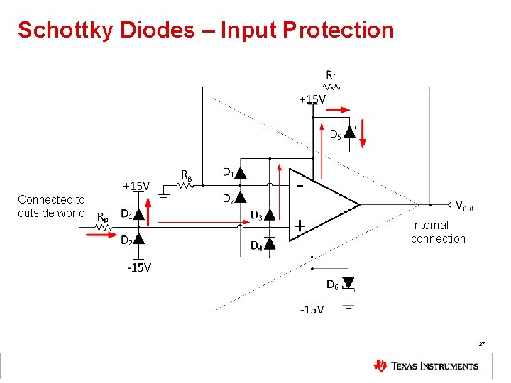
Schottky Diodes – Input Protection Connected to outside world Internal connection 27
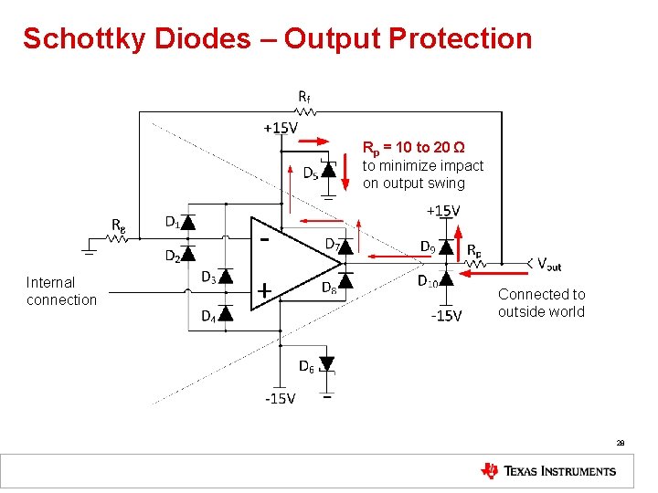
Schottky Diodes – Output Protection Rp = 10 to 20 Ω to minimize impact on output swing Internal connection Connected to outside world 28
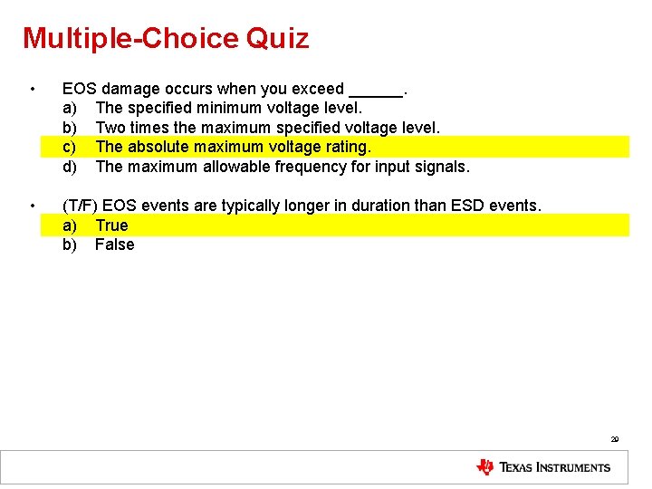
Multiple-Choice Quiz • EOS damage occurs when you exceed ______. a) The specified minimum voltage level. b) Two times the maximum specified voltage level. c) The absolute maximum voltage rating. d) The maximum allowable frequency for input signals. • (T/F) EOS events are typically longer in duration than ESD events. a) True b) False 29
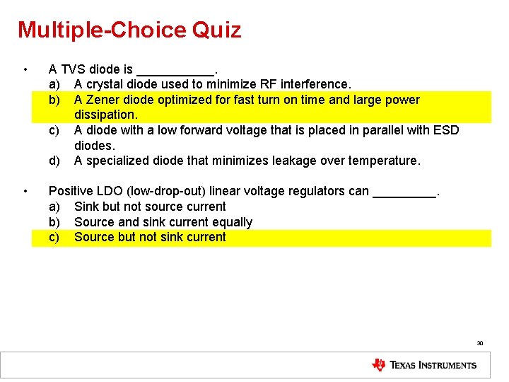
Multiple-Choice Quiz • A TVS diode is ______. a) A crystal diode used to minimize RF interference. b) A Zener diode optimized for fast turn on time and large power dissipation. c) A diode with a low forward voltage that is placed in parallel with ESD diodes. d) A specialized diode that minimizes leakage over temperature. • Positive LDO (low-drop-out) linear voltage regulators can _____. a) Sink but not source current b) Source and sink current equally c) Source but not sink current 30
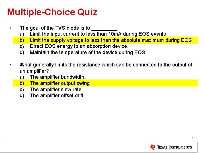
Multiple-Choice Quiz • The goal of the TVS diode is to _____. a) Limit the input current to less than 10 m. A during EOS events b) Limit the supply voltage to less than the absolute maximum during EOS c) Direct EOS energy to an absorption device. d) Maintain the temperature of the device during EOS • What generally limits the resistance which can be connected to the output of an amplifier? a) The amplifier bandwidth. b) The amplifier output swing c) The amplifier slew rate d) The amplifier offset drift. 31
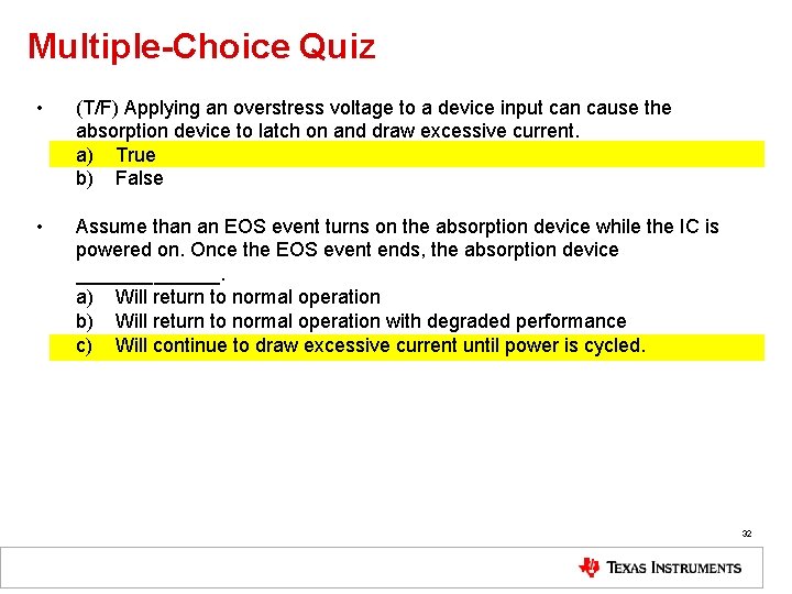
Multiple-Choice Quiz • (T/F) Applying an overstress voltage to a device input can cause the absorption device to latch on and draw excessive current. a) True b) False • Assume than an EOS event turns on the absorption device while the IC is powered on. Once the EOS event ends, the absorption device _______. a) Will return to normal operation b) Will return to normal operation with degraded performance c) Will continue to draw excessive current until power is cycled. 32

Thanks for your time! 33
- Slides: 33