Electronics Principles Applications Sixth Edition Charles A Schuler
- Slides: 62

Electronics Principles & Applications Sixth Edition Charles A. Schuler Chapter 9 Operational Amplifiers © 2003 Glencoe/Mc. Graw-Hill

INTRODUCTION • The Differential Amplifier • The Operational Amplifier • Determining Gain • Frequency Effects • Applications • Comparators

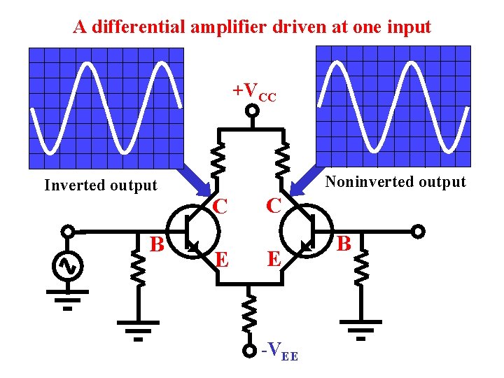
A differential amplifier driven at one input +VCC Inverted output B Noninverted output C E -VEE B

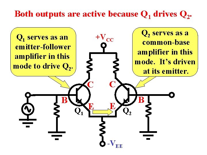
Both outputs are active because Q 1 drives Q 2. Q 1 serves as an emitter-follower amplifier in this mode to drive Q 2. +VCC C B Q 1 E Q 2 serves as a common-base amplifier in this mode. It’s driven at its emitter. C E Q 2 -VEE B

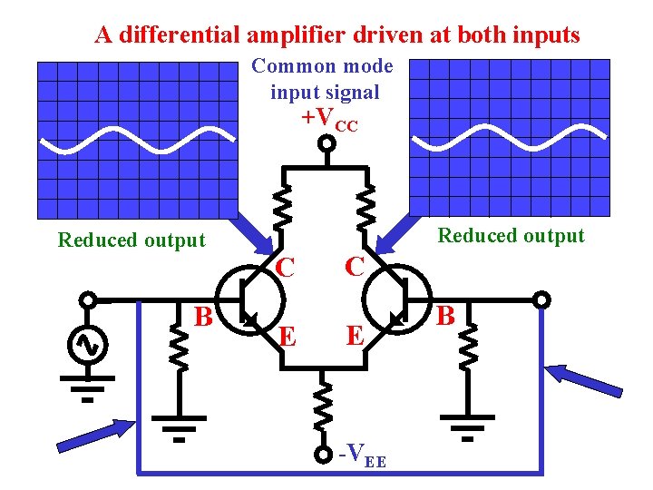
A differential amplifier driven at both inputs Common mode input signal +VCC Reduced output B Reduced output C E -VEE B

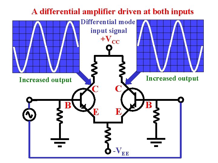
A differential amplifier driven at both inputs Differential mode input signal +VCC Increased output B Increased output C E -VEE B

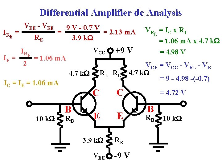
Differential Amplifier dc Analysis IR = VEE - VBE RE E IE = IR 2 E 9 V - 0. 7 V = 2. 13 m. A = 3. 9 k. W VCC = 1. 06 m. A 4. 7 k. W IC = IE = 1. 06 m. A 10 k. W B RB +9 V RL RL C E 3. 9 k. W VEE VR = I C x RL L = 1. 06 m. A x 4. 7 k. W = 4. 98 V VCE = VCC - VRL - VE 4. 7 k. W = 9 - 4. 98 -(-0. 7) C E RE -9 V = 4. 72 V B RB 10 k. W

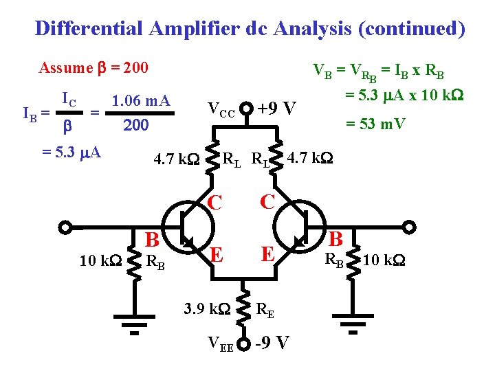
Differential Amplifier dc Analysis (continued) Assume b = 200 IB = IC b VB = V R = I B x RB B 1. 06 m. A = 200 = 5. 3 m. A VCC 4. 7 k. W 10 k. W RB +9 V = 53 m. V RL RL 4. 7 k. W C B = 5. 3 m. A x 10 k. W E 3. 9 k. W VEE C E RE -9 V B RB 10 k. W

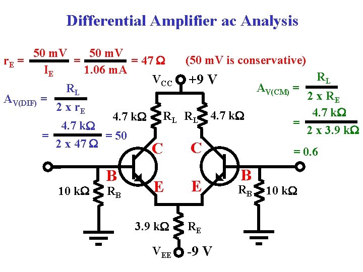
Differential Amplifier ac Analysis 50 m. V (50 m. V is conservative) = 47 W = r. E = IE 1. 06 m. A RL VCC +9 V AV(CM) = RL 2 x RE AV(DIF) = 2 x r. E 4. 7 k. W RL RL 4. 7 k. W = 4. 7 k. W 2 x 3. 9 k. W = = 50 2 x 47 W C C = 0. 6 10 k. W B RB E 3. 9 k. W VEE E RE -9 V B RB 10 k. W

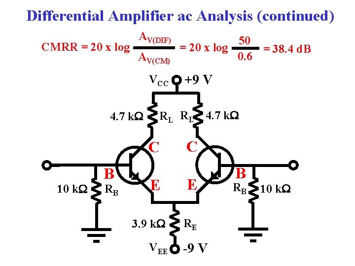
Differential Amplifier ac Analysis (continued) CMRR = 20 x log AV(DIF) AV(CM) VCC 4. 7 k. W 10 k. W RB +9 V RL RL 4. 7 k. W C B 50 = 20 x log = 38. 4 d. B 0. 6 E 3. 9 k. W VEE C E RE -9 V B RB 10 k. W

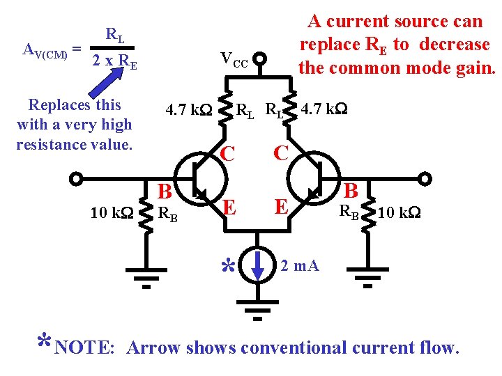
AV(CM) = A current source can replace RE to decrease the common mode gain. RL VCC 2 x RE Replaces this with a very high resistance value. 10 k. W 4. 7 k. W RL RL 4. 7 k. W C B RB E * C E B RB 10 k. W 2 m. A *NOTE: Arrow shows conventional current flow.

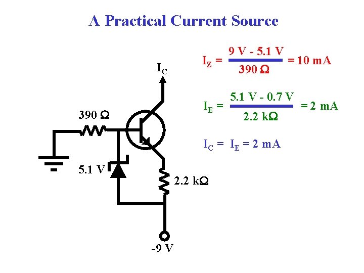
A Practical Current Source IC 9 V - 5. 1 V IZ = = 10 m. A 390 W IE = 390 W 5. 1 V - 0. 7 V 2. 2 k. W IC = IE = 2 m. A 5. 1 V 2. 2 k. W -9 V = 2 m. A

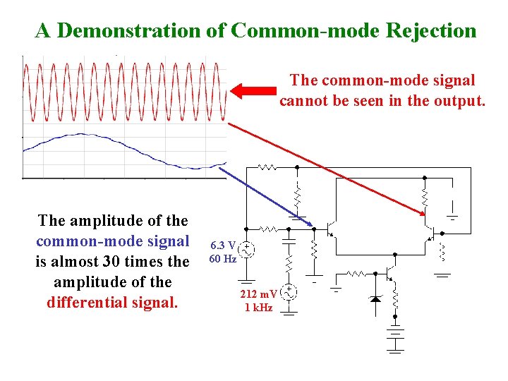
A Demonstration of Common-mode Rejection The common-mode signal cannot be seen in the output. The amplitude of the common-mode signal is almost 30 times the amplitude of the differential signal. 6. 3 V 60 Hz 212 m. V 1 k. Hz

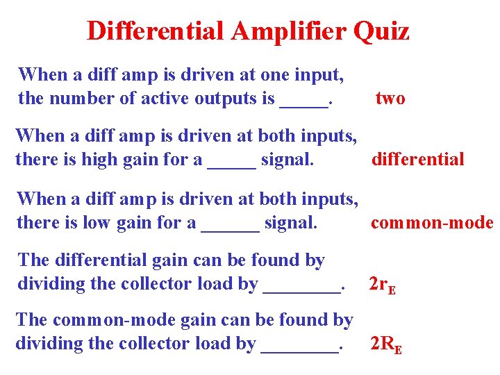
Differential Amplifier Quiz When a diff amp is driven at one input, the number of active outputs is _____. two When a diff amp is driven at both inputs, there is high gain for a _____ signal. differential When a diff amp is driven at both inputs, there is low gain for a ______ signal. common-mode The differential gain can be found by dividing the collector load by ____. 2 r. E The common-mode gain can be found by dividing the collector load by ____. 2 RE

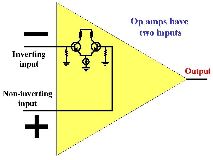
Op amps have two inputs Inverting input Non-inverting input Output

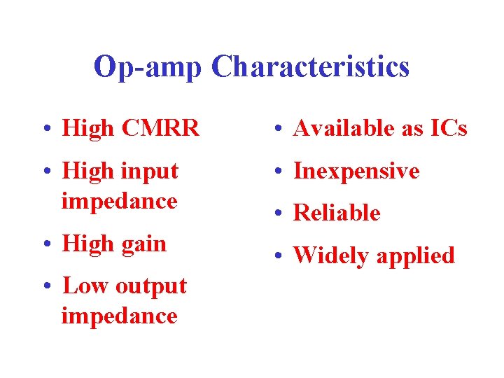
Op-amp Characteristics • High CMRR • Available as ICs • High input impedance • Inexpensive • High gain • Widely applied • Low output impedance • Reliable

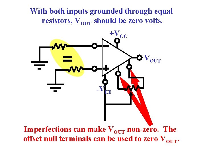
With both inputs grounded through equal resistors, VOUT should be zero volts. +VCC VOUT -VEE Imperfections can make VOUT non-zero. The offset null terminals can be used to zero VOUT.

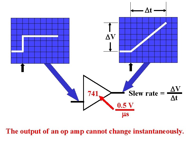
Dt DV 741 DV Slew rate = Dt 0. 5 V ms The output of an op amp cannot change instantaneously.

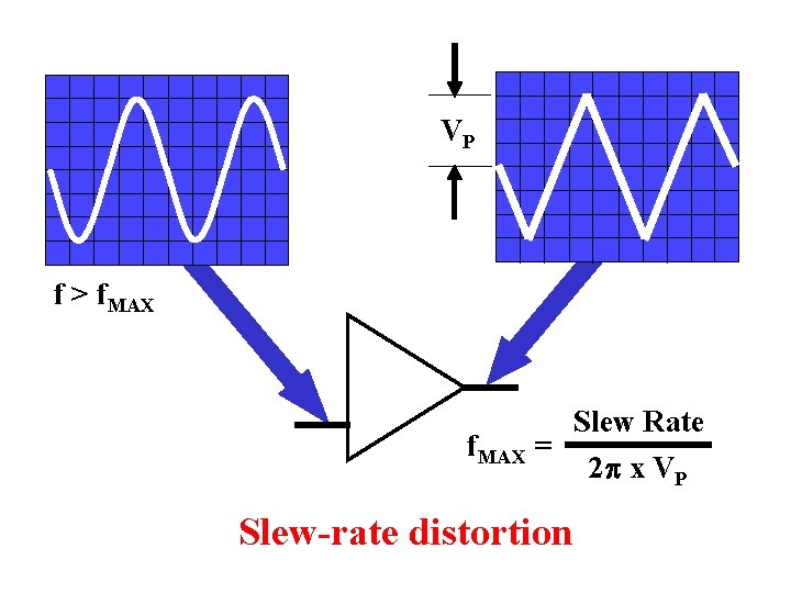
VP f > f. MAX = Slew-rate distortion Slew Rate 2 p x VP

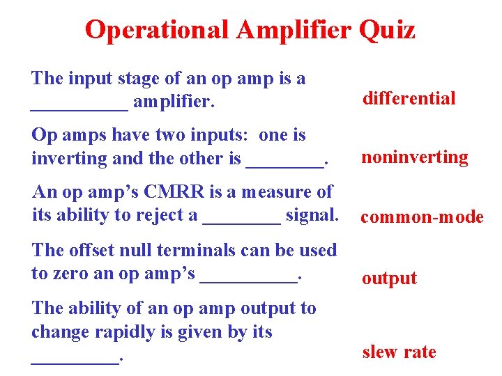
Operational Amplifier Quiz The input stage of an op amp is a _____ amplifier. differential Op amps have two inputs: one is inverting and the other is ____. noninverting An op amp’s CMRR is a measure of its ability to reject a ____ signal. common-mode The offset null terminals can be used to zero an op amp’s _____. output The ability of an op amp output to change rapidly is given by its _____. slew rate

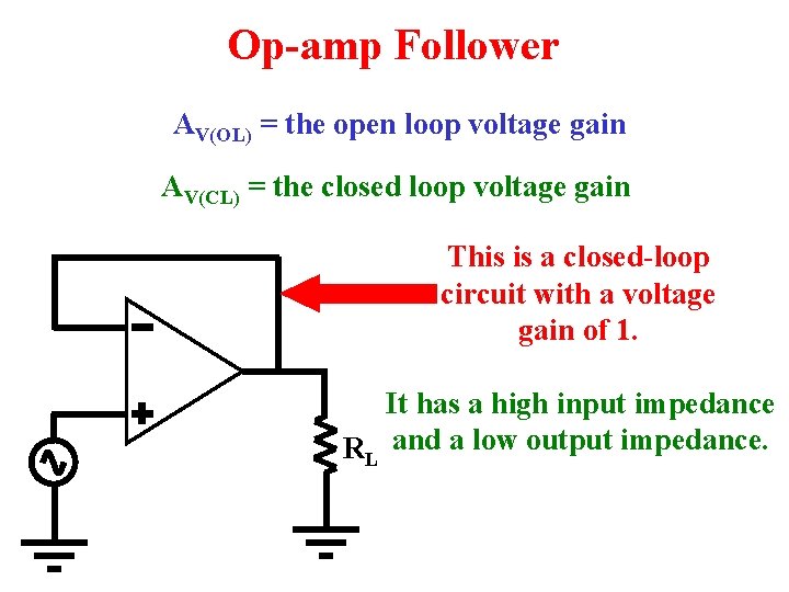
Op-amp Follower AV(OL) = the open loop voltage gain AV(CL) = the closed loop voltage gain This is a closed-loop circuit with a voltage gain of 1. It has a high input impedance RL and a low output impedance.

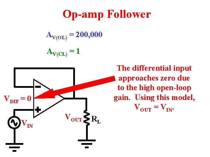
Op-amp Follower AV(OL) = 200, 000 AV(CL) = 1 The differential input approaches zero due to the high open-loop gain. Using this model, VOUT = VIN. VDIF = 0 VIN VOUT RL

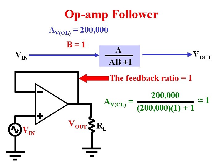
Op-amp Follower AV(OL) = 200, 000 B=1 A AB +1 VIN VOUT The feedback ratio = 1 200, 000 @1 AV(CL) = (200, 000)(1) + 1 VIN VOUT RL

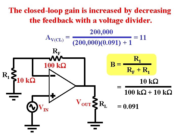
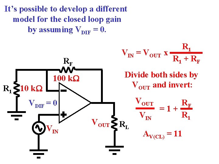
The closed-loop gain is increased by decreasing the feedback with a voltage divider. R 1 200, 000 AV(CL) = = 11 (200, 000)(0. 091) + 1 RF R 1 B= 100 k. W RF + R 1 10 k. W = VIN VOUT RL 10 k. W 100 k. W + 10 k. W = 0. 091

It’s possible to develop a different model for the closed loop gain by assuming VDIF = 0. R 1 VIN = VOUT x R 1 + R F RF Divide both sides by VOUT and invert: 100 k. W R 1 10 k. W VOUT VDIF = 0 VIN VOUT RL VIN RF =1+ R 1 AV(CL) = 11

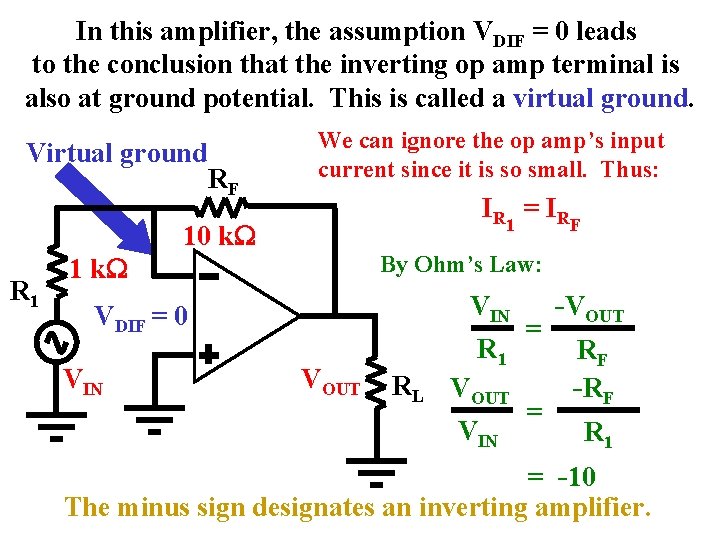
In this amplifier, the assumption VDIF = 0 leads to the conclusion that the inverting op amp terminal is also at ground potential. This is called a virtual ground. Virtual ground RF We can ignore the op amp’s input current since it is so small. Thus: IR = I R 1 10 k. W R 1 By Ohm’s Law: 1 k. W VIN VDIF = 0 VIN F VOUT R 1 RL VOUT VIN = = -VOUT RF -R F R 1 = -10 The minus sign designates an inverting amplifier.

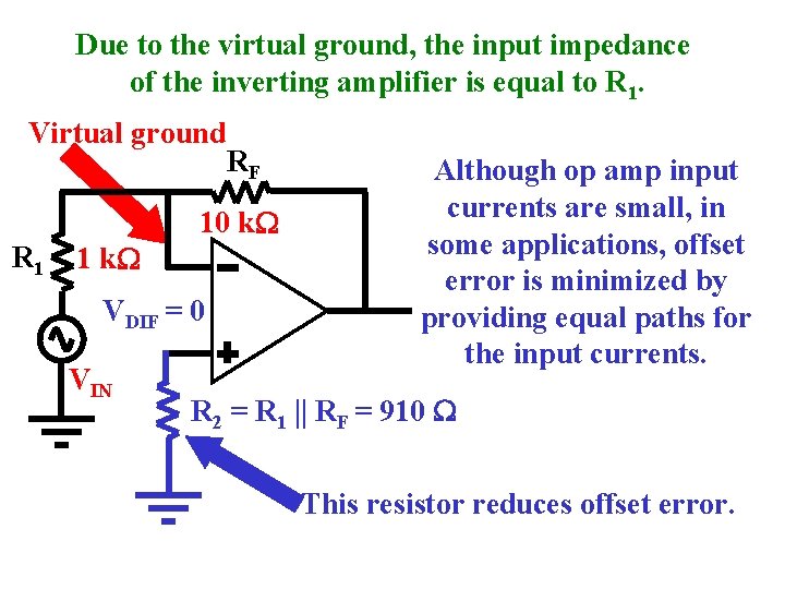
Due to the virtual ground, the input impedance of the inverting amplifier is equal to R 1. Virtual ground RF 10 k. W R 1 1 k. W VDIF = 0 VIN Although op amp input currents are small, in some applications, offset error is minimized by providing equal paths for the input currents. R 2 = R 1 || RF = 910 W This resistor reduces offset error.

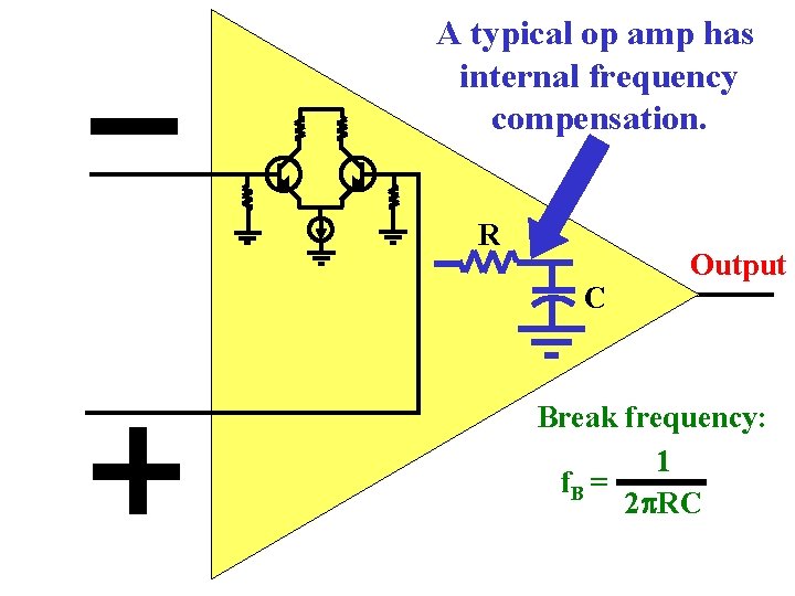
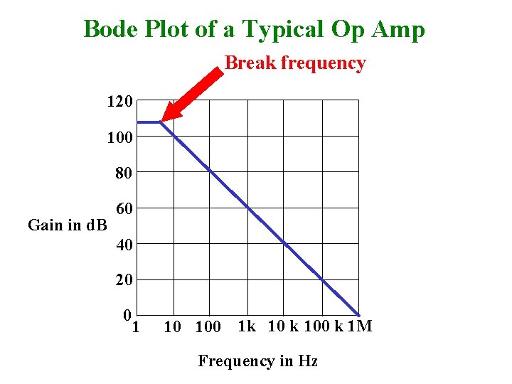
A typical op amp has internal frequency compensation. R C Output Break frequency: 1 f. B = 2 p. RC

Bode Plot of a Typical Op Amp Break frequency 120 100 80 Gain in d. B 60 40 20 0 1 10 100 1 k 100 k 1 M Frequency in Hz

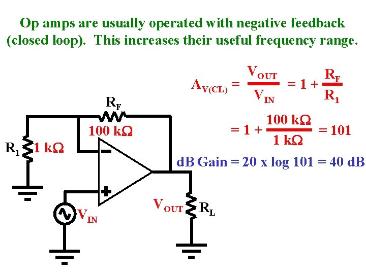
Op amps are usually operated with negative feedback (closed loop). This increases their useful frequency range. AV(CL) = RF VIN RF =1+ R 1 100 k. W =1+ = 101 1 k. W 100 k. W R 1 1 k. W VOUT d. B Gain = 20 x log 101 = 40 d. B VIN VOUT RL

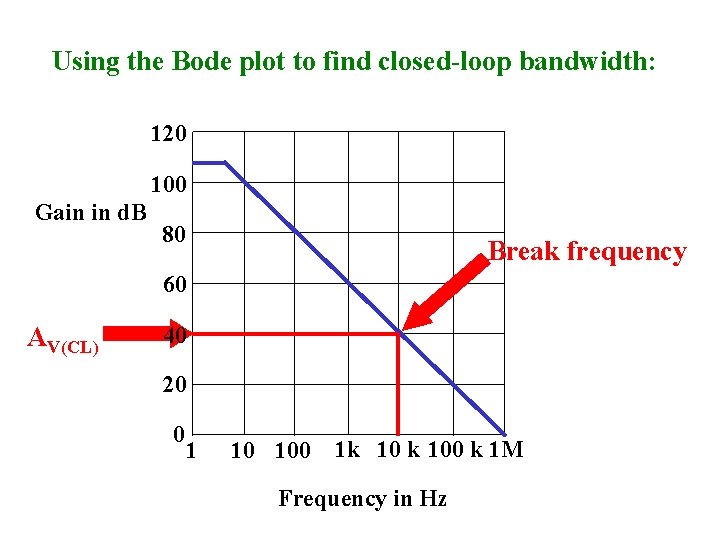
Using the Bode plot to find closed-loop bandwidth: 120 100 Gain in d. B 80 Break frequency 60 AV(CL) 40 20 0 1 10 100 1 k 100 k 1 M Frequency in Hz

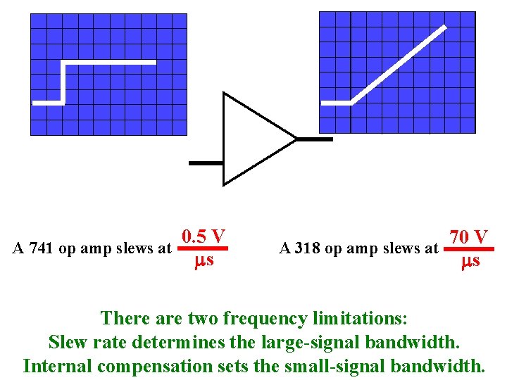
A 741 op amp slews at 0. 5 V ms 70 V A 318 op amp slews at ms There are two frequency limitations: Slew rate determines the large-signal bandwidth. Internal compensation sets the small-signal bandwidth.

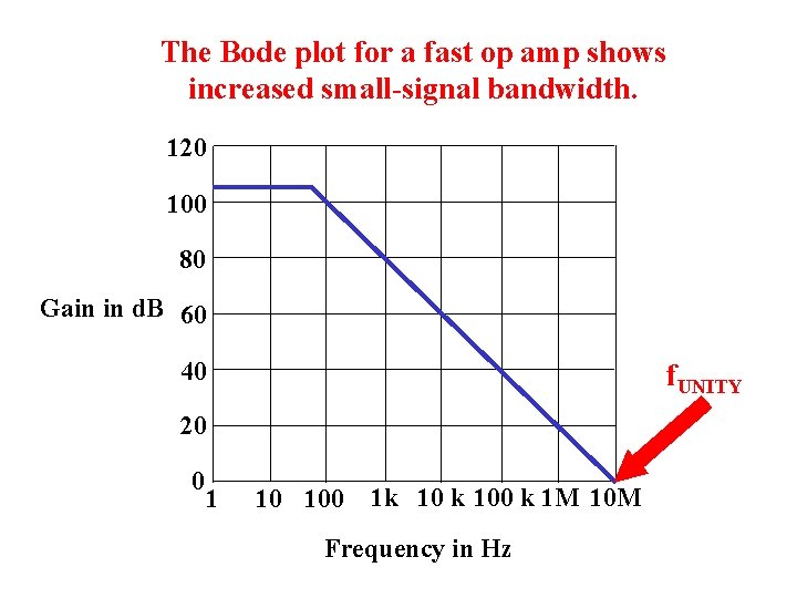
The Bode plot for a fast op amp shows increased small-signal bandwidth. 120 100 80 Gain in d. B 60 40 f. UNITY 20 0 1 10 100 1 k 100 k 1 M 10 M Frequency in Hz

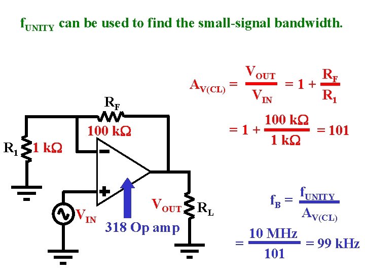
f. UNITY can be used to find the small-signal bandwidth. AV(CL) = RF VIN RF =1+ R 1 100 k. W =1+ = 101 1 k. W 100 k. W R 1 1 k. W VIN VOUT 318 Op amp RL f. UNITY f. B = AV(CL) 10 MHz = = 99 k. Hz 101

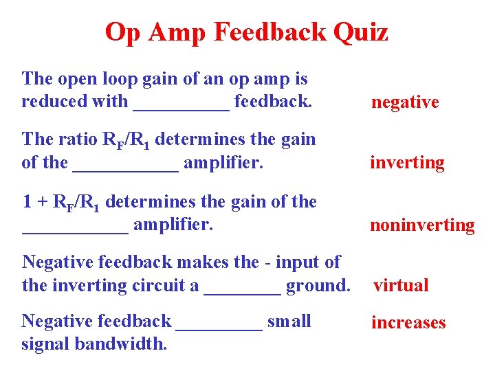
Op Amp Feedback Quiz The open loop gain of an op amp is reduced with _____ feedback. negative The ratio RF/R 1 determines the gain of the ______ amplifier. inverting 1 + RF/R 1 determines the gain of the ______ amplifier. noninverting Negative feedback makes the - input of the inverting circuit a ____ ground. virtual Negative feedback _____ small signal bandwidth. increases

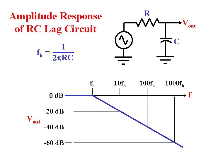
R Amplitude Response of RC Lag Circuit Vout C 1 fb = 2 p. RC fb 0 d. B Vout -20 d. B -40 d. B -60 d. B 10 fb 1000 fb f

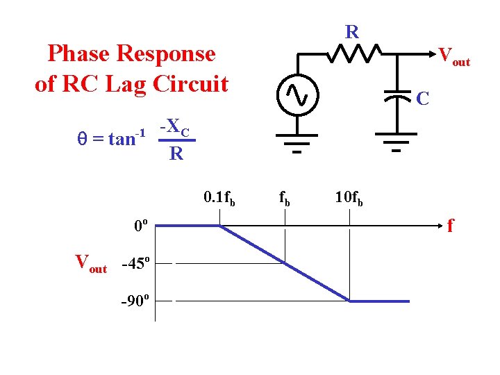
R Phase Response of RC Lag Circuit = tan -1 Vout -45 o -90 o C -XC R 0. 1 fb 0 o Vout fb 10 fb f

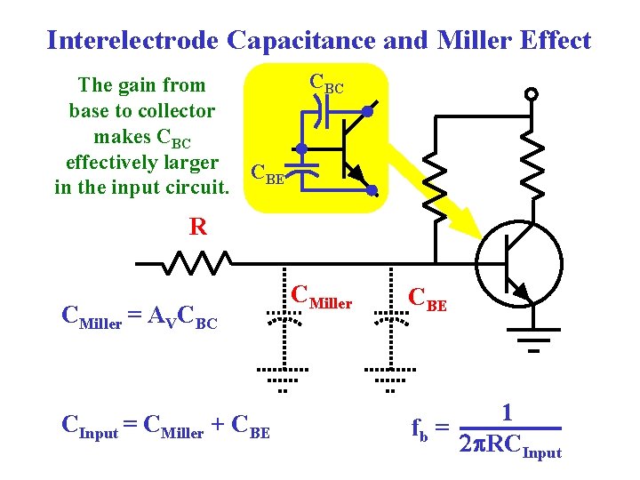
Interelectrode Capacitance and Miller Effect The gain from base to collector makes CBC effectively larger C BE in the input circuit. CBC R CMiller = AVCBC CInput = CMiller + CBE CMiller CBE 1 fb = 2 p. RCInput

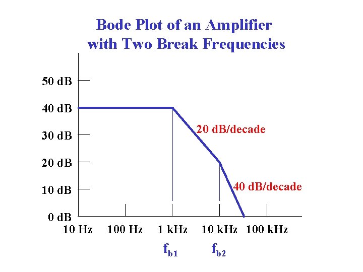
Bode Plot of an Amplifier with Two Break Frequencies 50 d. B 40 d. B 20 d. B/decade 30 d. B 20 d. B 40 d. B/decade 10 d. B 10 Hz 100 Hz 1 k. Hz fb 1 10 k. Hz 100 k. Hz fb 2

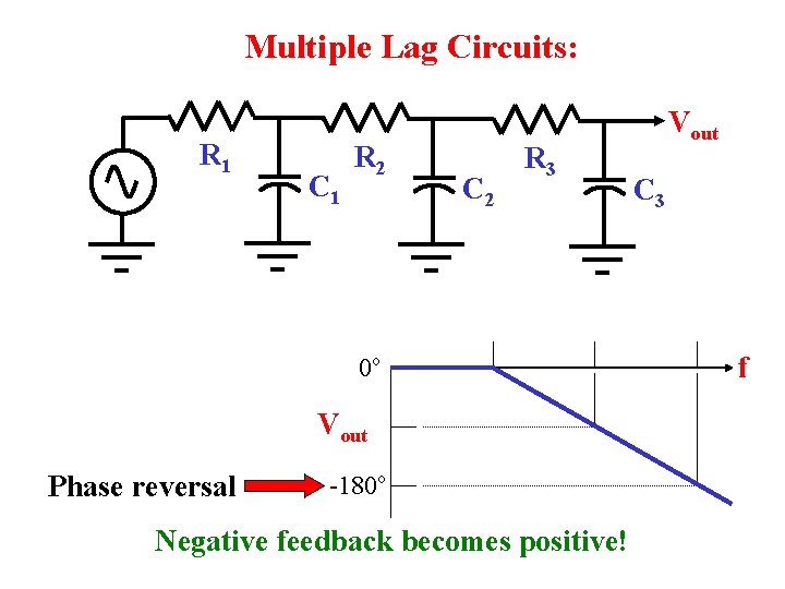
Multiple Lag Circuits: R 1 C 1 R 2 C 2 R 3 0 o Vout Phase reversal -180 o Negative feedback becomes positive! Vout C 3 f

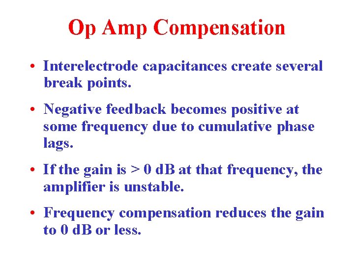
Op Amp Compensation • Interelectrode capacitances create several break points. • Negative feedback becomes positive at some frequency due to cumulative phase lags. • If the gain is > 0 d. B at that frequency, the amplifier is unstable. • Frequency compensation reduces the gain to 0 d. B or less.

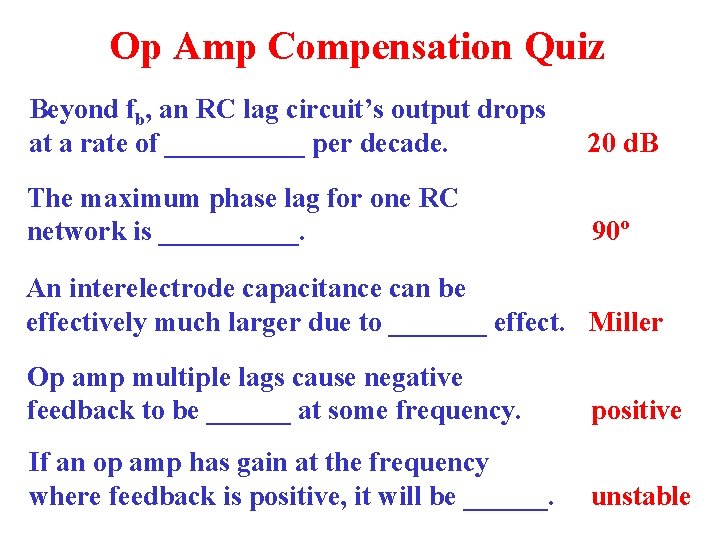
Op Amp Compensation Quiz Beyond fb, an RC lag circuit’s output drops at a rate of _____ per decade. 20 d. B The maximum phase lag for one RC network is _____. 90 o An interelectrode capacitance can be effectively much larger due to _______ effect. Miller Op amp multiple lags cause negative feedback to be ______ at some frequency. positive If an op amp has gain at the frequency where feedback is positive, it will be ______. unstable

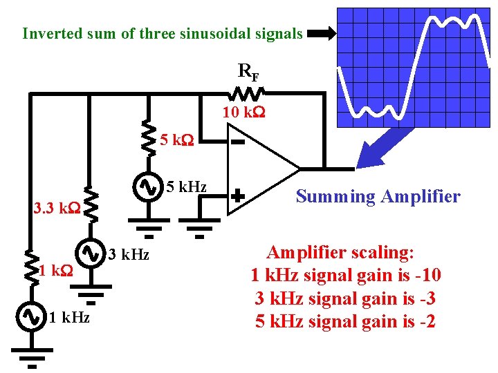
Inverted sum of three sinusoidal signals RF 10 k. W 5 k. Hz 3. 3 k. W 1 k. Hz 3 k. Hz Summing Amplifier scaling: 1 k. Hz signal gain is -10 3 k. Hz signal gain is -3 5 k. Hz signal gain is -2

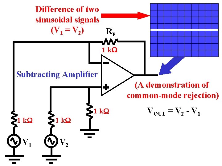
Difference of two sinusoidal signals (V 1 = V 2) RF 1 k. W Subtracting Amplifier (A demonstration of common-mode rejection) 1 k. W V 1 V 2 VOUT = V 2 - V 1

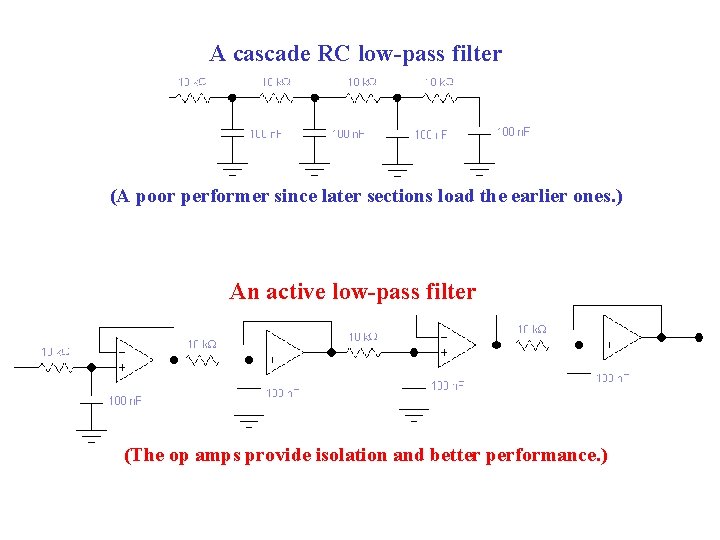
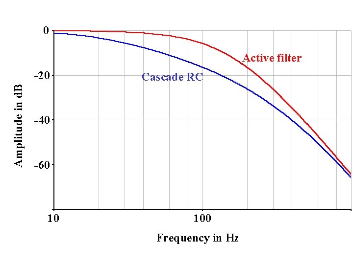
A cascade RC low-pass filter (A poor performer since later sections load the earlier ones. ) An active low-pass filter (The op amps provide isolation and better performance. )

0 Active filter Amplitude in d. B -20 Cascade RC -40 -60 10 100 Frequency in Hz

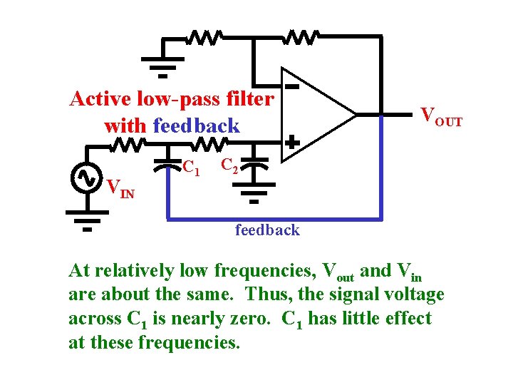
Active low-pass filter with feedback VIN C 1 VOUT C 2 feedback At relatively low frequencies, Vout and Vin are about the same. Thus, the signal voltage across C 1 is nearly zero. C 1 has little effect at these frequencies.

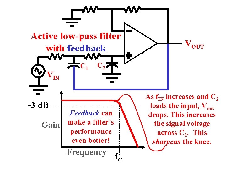
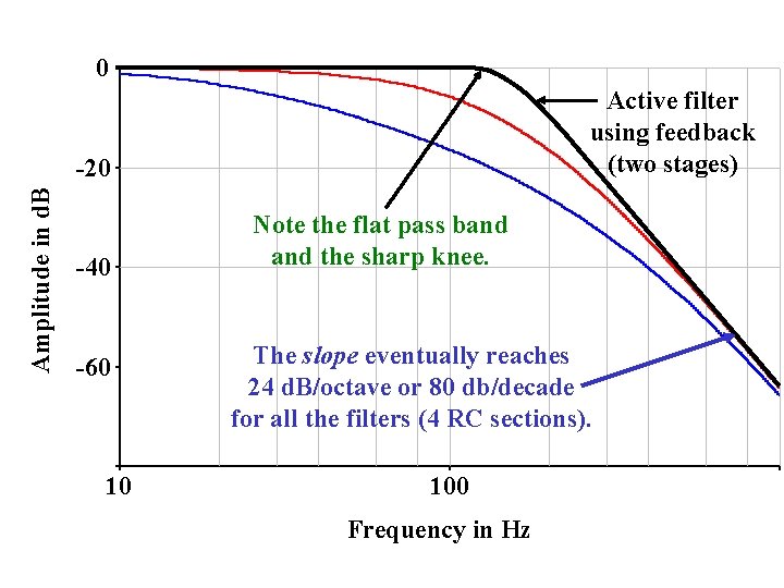
Active low-pass filter with feedback VIN -3 d. B Gain C 1 VOUT C 2 Feedback can make a filter’s performance even better! Frequency f C As f. IN increases and C 2 loads the input, Vout drops. This increases the signal voltage across C 1. This sharpens the knee.

0 Active filter using feedback (two stages) Amplitude in d. B -20 -40 -60 10 Note the flat pass band the sharp knee. The slope eventually reaches 24 d. B/octave or 80 db/decade for all the filters (4 RC sections). 100 Frequency in Hz

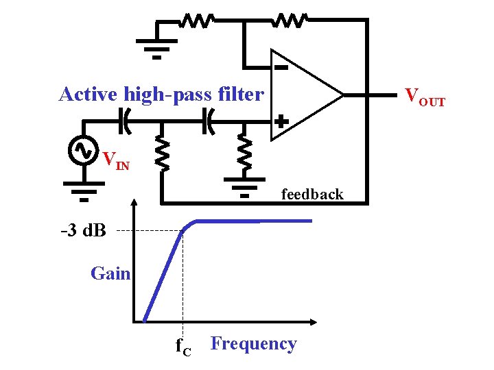
Active high-pass filter VOUT VIN feedback -3 d. B Gain f. C Frequency

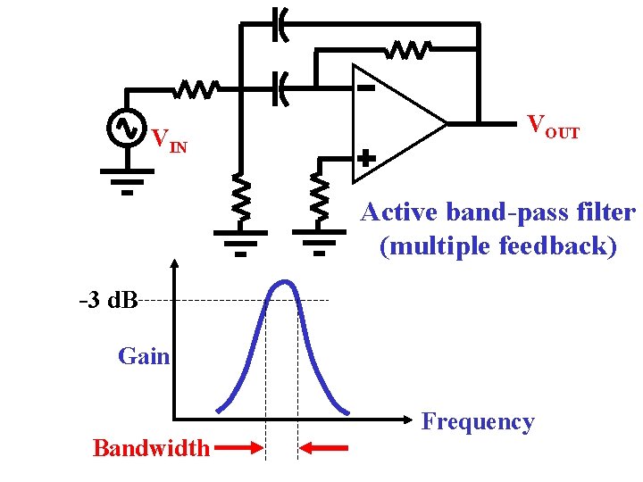
VIN VOUT Active band-pass filter (multiple feedback) -3 d. B Gain Bandwidth Frequency

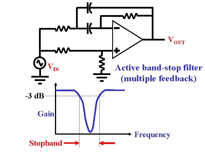
VOUT VIN Active band-stop filter (multiple feedback) -3 d. B Gain Stopband Frequency

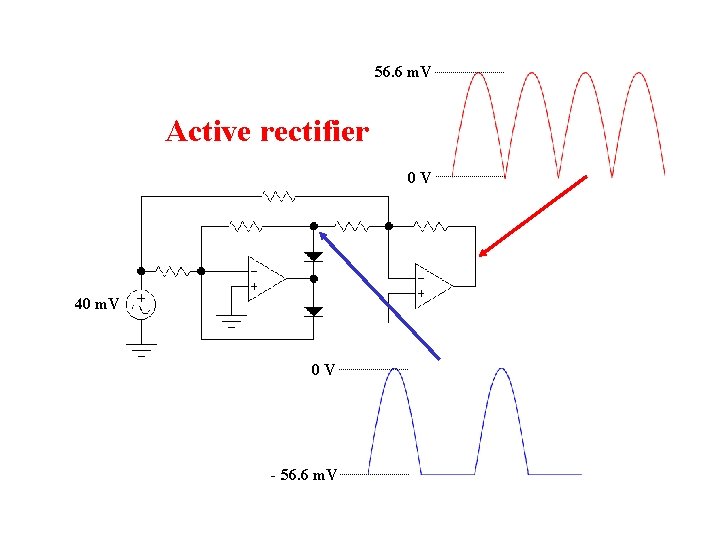
56. 6 m. V Active rectifier 0 V 40 m. V 0 V - 56. 6 m. V

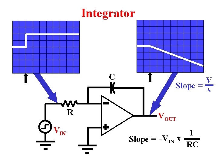
Integrator C R VIN V Slope = s VOUT 1 Slope = -VIN x RC

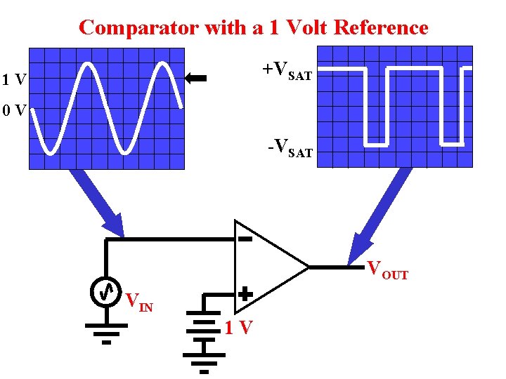
Comparator with a 1 Volt Reference +VSAT 1 V 0 V -VSAT VOUT VIN 1 V

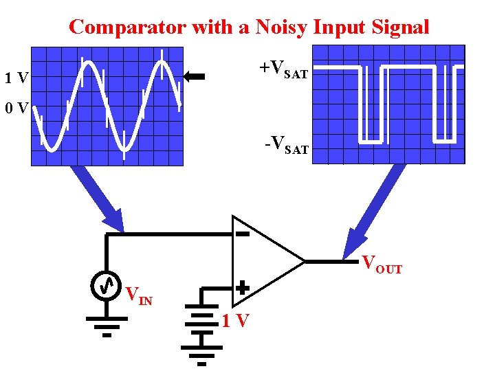
Comparator with a Noisy Input Signal +VSAT 1 V 0 V -VSAT VOUT VIN 1 V

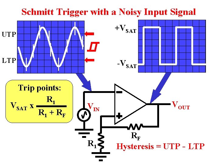
Schmitt Trigger with a Noisy Input Signal +VSAT UTP LTP Trip points: R 1 VSAT x R 1 + R F -VSAT VIN R 1 VOUT RF Hysteresis = UTP - LTP

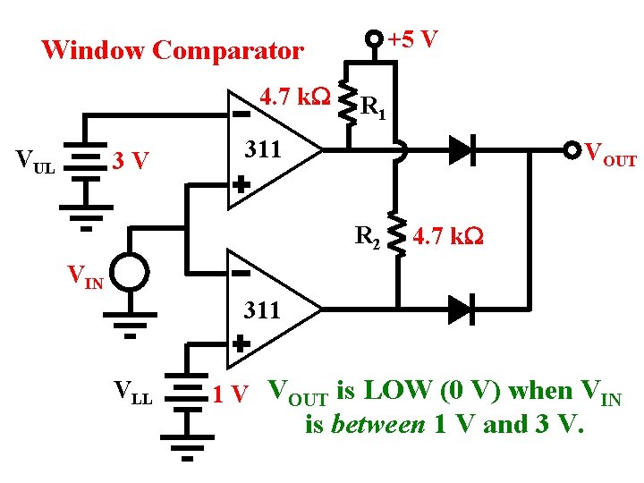
+5 V Window Comparator 4. 7 k. W VUL 3 V R 1 311 VOUT R 2 4. 7 k. W VIN 311 VLL 1 V VOUT is LOW (0 V) when VIN is between 1 V and 3 V.

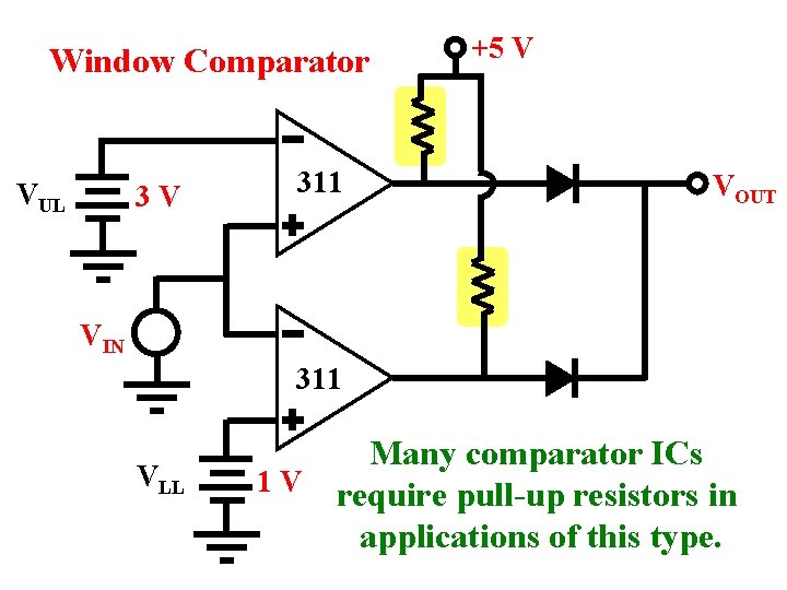
Window Comparator VUL 3 V 311 +5 V VOUT VIN 311 VLL Many comparator ICs 1 V require pull-up resistors in applications of this type.

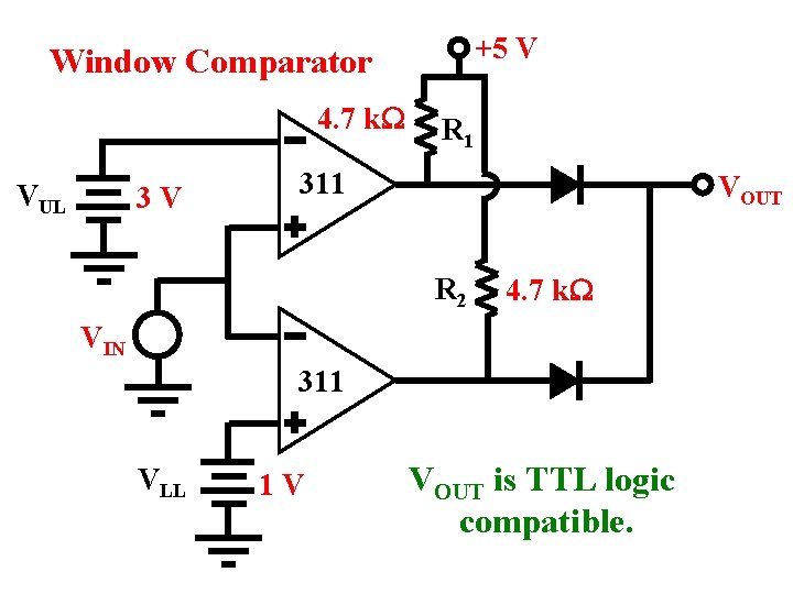
+5 V Window Comparator 4. 7 k. W VUL 3 V R 1 311 VOUT R 2 4. 7 k. W VIN 311 VLL 1 V VOUT is TTL logic compatible.

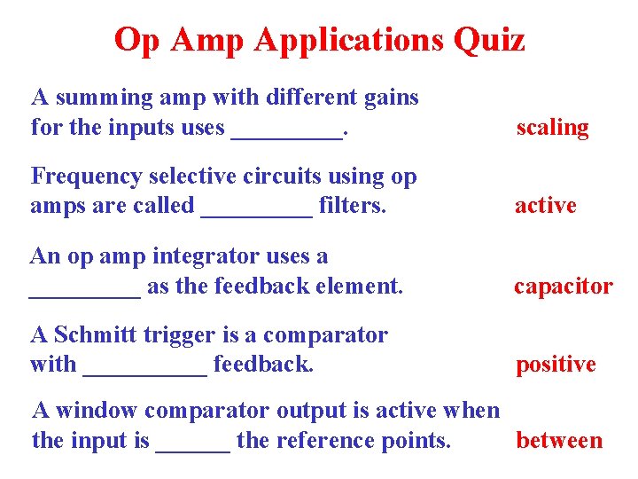
Op Amp Applications Quiz A summing amp with different gains for the inputs uses _____. scaling Frequency selective circuits using op amps are called _____ filters. active An op amp integrator uses a _____ as the feedback element. capacitor A Schmitt trigger is a comparator with _____ feedback. positive A window comparator output is active when the input is ______ the reference points. between

REVIEW • The Differential Amplifier • The Operational Amplifier • Determining Gain • Frequency Effects • Applications • Comparators