Electronics Lab 20 260 465 Transistor Switching Characteristics
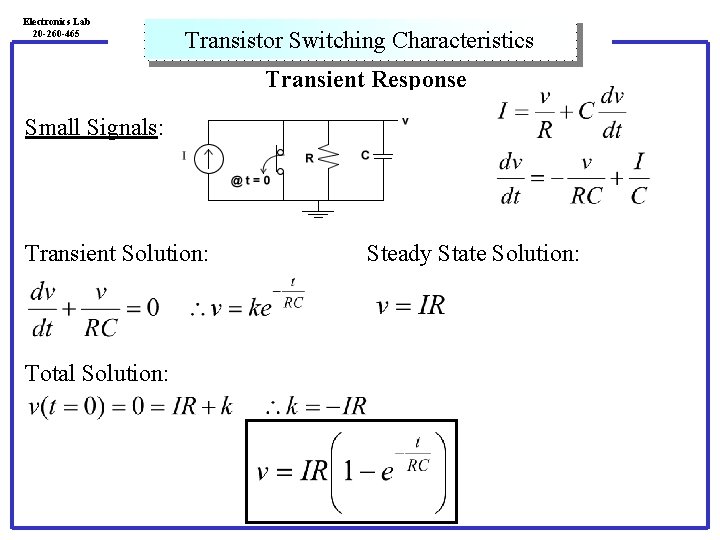
Electronics Lab 20 -260 -465 Transistor Switching Characteristics Transient Response Small Signals: Transient Solution: Total Solution: Steady State Solution:
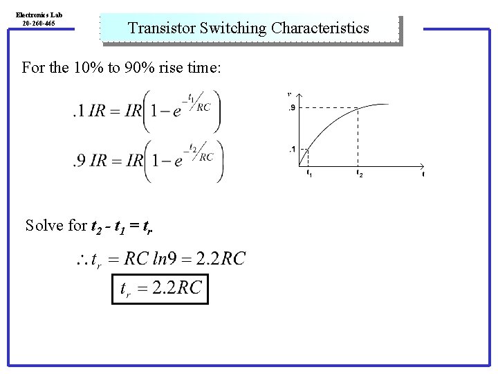
Electronics Lab 20 -260 -465 Transistor Switching Characteristics For the 10% to 90% rise time: Solve for t 2 - t 1 = tr
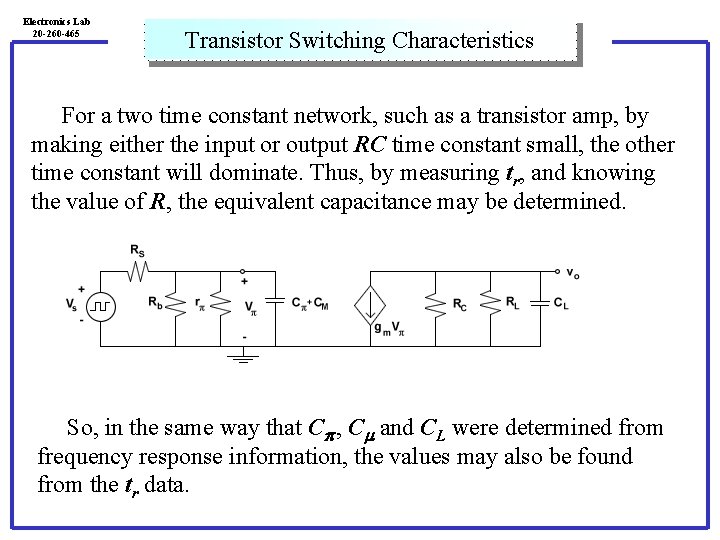
Electronics Lab 20 -260 -465 Transistor Switching Characteristics For a two time constant network, such as a transistor amp, by making either the input or output RC time constant small, the other time constant will dominate. Thus, by measuring tr, and knowing the value of R, the equivalent capacitance may be determined. So, in the same way that Cp , Cm and CL were determined from frequency response information, the values may also be found from the tr data.
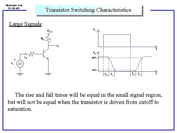
Electronics Lab 20 -260 -465 Transistor Switching Characteristics Large Signals: The rise and fall times will be equal in the small signal region, but will not be equal when the transistor is driven from cutoff to saturation.
Electronics Lab 20 -260 -465 Transistor Switching Characteristics 1) The fall time will be shorter because as long as v. C is falling and hasn’t reached VCE, SAT, then i. C= i. B and for large i. B, there is thus more i. C to discharge load capacitances. Thus as i. B is increased to levels beyond i. C, max / , i. e. overdrive, the fall time decreases with increasing overdrive.
Electronics Lab 20 -260 -465 Transistor Switching Characteristics 2) The storage time increases. This occurs because the excess current in the base causes charge storage in the base and collector regions, thus requiring a longer time period for removal, which is the reason for the storage time. This increases with overdrive. There is also a minor third effect, namely that the delay time decreases with overdrive. It is often small anyway and this may not be a noticeable effect.
- Slides: 6