Electronics Lab 20 260 465 Junction Field Effect
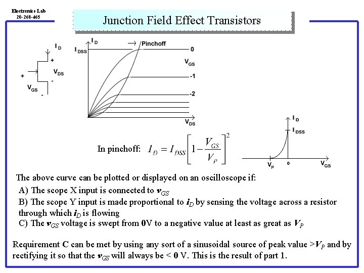
Electronics Lab 20 -260 -465 Junction Field Effect Transistors In pinchoff: The above curve can be plotted or displayed on an oscilloscope if: A) The scope X input is connected to v. GS B) The scope Y input is made proportional to i. D by sensing the voltage across a resistor through which i. D is flowing C) The v. GS voltage is swept from 0 V to a negative value at least as great as VP Requirement C can be met by using any sort of a sinusoidal source of peak value >VP and by rectifying it so that the v. GS will always be < 0 V. This is the result of part 1.
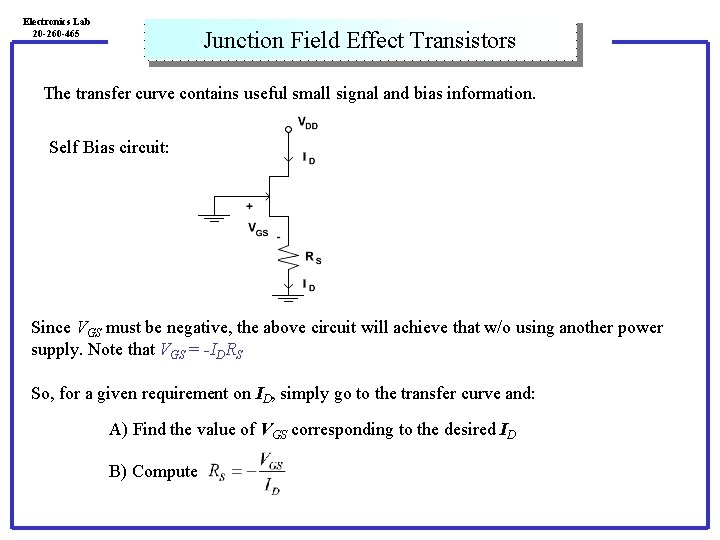
Electronics Lab 20 -260 -465 Junction Field Effect Transistors The transfer curve contains useful small signal and bias information. Self Bias circuit: Since VGS must be negative, the above circuit will achieve that w/o using another power supply. Note that VGS = -IDRS So, for a given requirement on ID, simply go to the transfer curve and: A) Find the value of VGS corresponding to the desired ID B) Compute
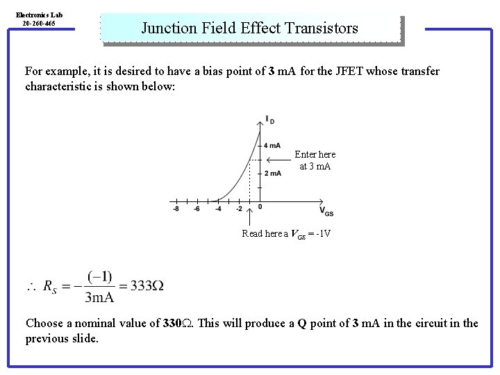
Electronics Lab 20 -260 -465 Junction Field Effect Transistors For example, it is desired to have a bias point of 3 m. A for the JFET whose transfer characteristic is shown below: Enter here at 3 m. A Read here a VGS = -1 V Choose a nominal value of 330 W. This will produce a Q point of 3 m. A in the circuit in the previous slide.
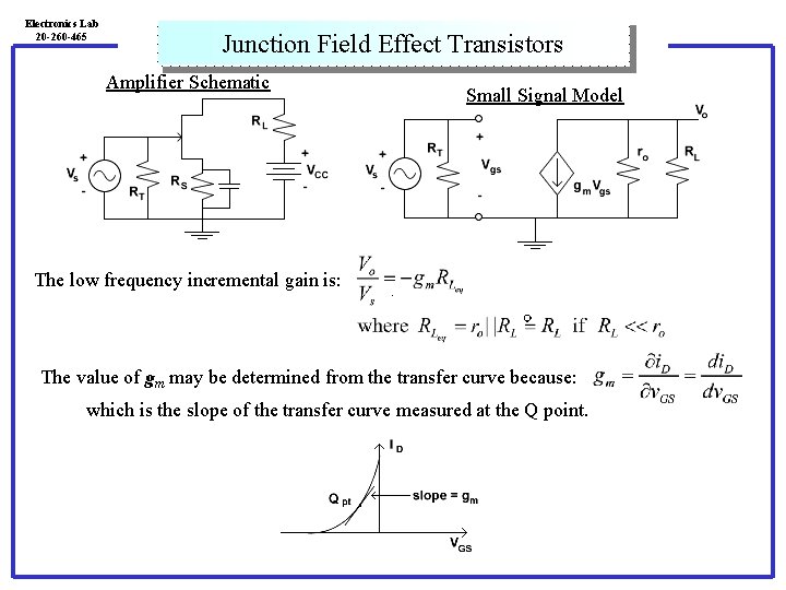
Electronics Lab 20 -260 -465 Junction Field Effect Transistors Amplifier Schematic Small Signal Model The low frequency incremental gain is: The value of gm may be determined from the transfer curve because: which is the slope of the transfer curve measured at the Q point.
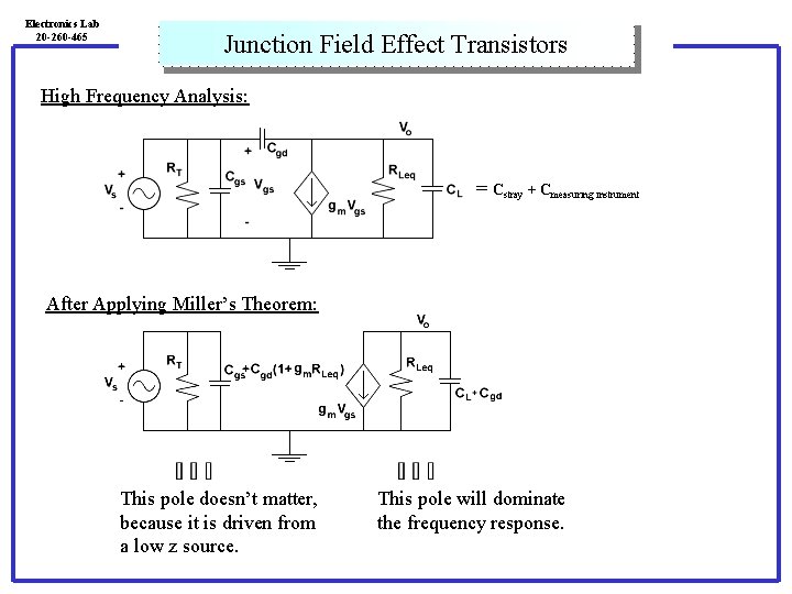
Electronics Lab 20 -260 -465 Junction Field Effect Transistors High Frequency Analysis: = Cstray + Cmeasuring instrument After Applying Miller’s Theorem: This pole doesn’t matter, because it is driven from a low z source. This pole will dominate the frequency response.
- Slides: 5