Electronics Evaluation and assessment Assignments Seminarsoral Quizzes Mid
- Slides: 25

Electronics

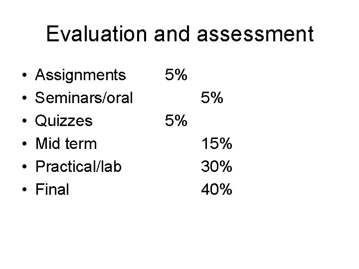
Evaluation and assessment • • • Assignments Seminars/oral Quizzes Mid term Practical/lab Final 5% 5% 5% 15% 30% 40%

Semiconductor Devices

Classification of Materials may be classified depend on its energy band structure into : • Insulators • Semiconductors • Metals

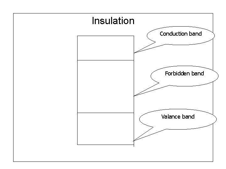
1 - Insulators • It is a very poor conductor of electricity. • The forbidden band which separates the valance band conduction band is very large ( order of 6 ) • The energy which can be supplied to an electron from an applied field is too small to carry the practice from the filled valance band to vacant conduction band • Example : Wood , Glass

Insulation Conduction band Forbidden band Valance band

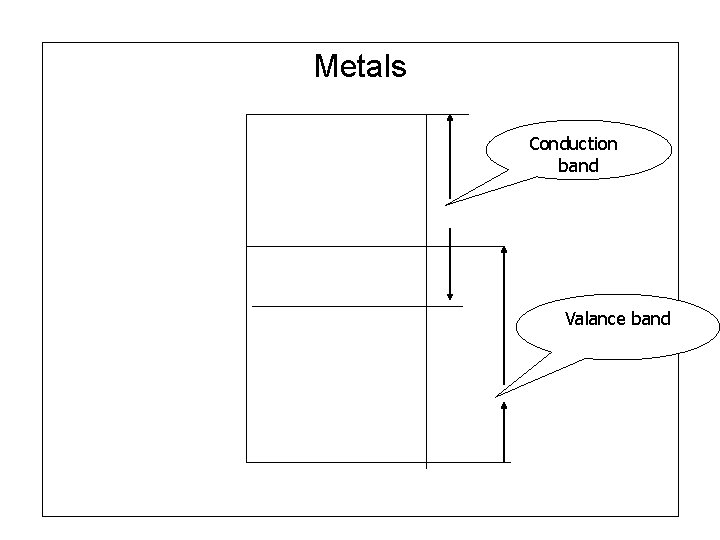
2 - Metals • It is an excellent conductor of electricity. • The filled valance band the empty conduction band overlap each other with no forbidden energy band. • Under the influence of an applied electric field, the electron acquire additional energy and move in to higher energy states. • Example : Copper , Silver, Aluminum.

Metals Conduction band Valance band

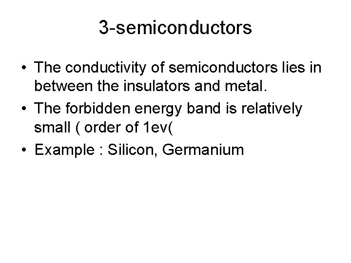
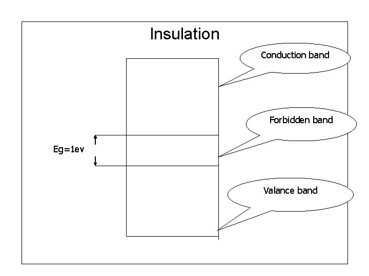
3 -semiconductors • The conductivity of semiconductors lies in between the insulators and metal. • The forbidden energy band is relatively small ( order of 1 ev( • Example : Silicon, Germanium

Insulation Conduction band Forbidden band Eg=1 ev Valance band

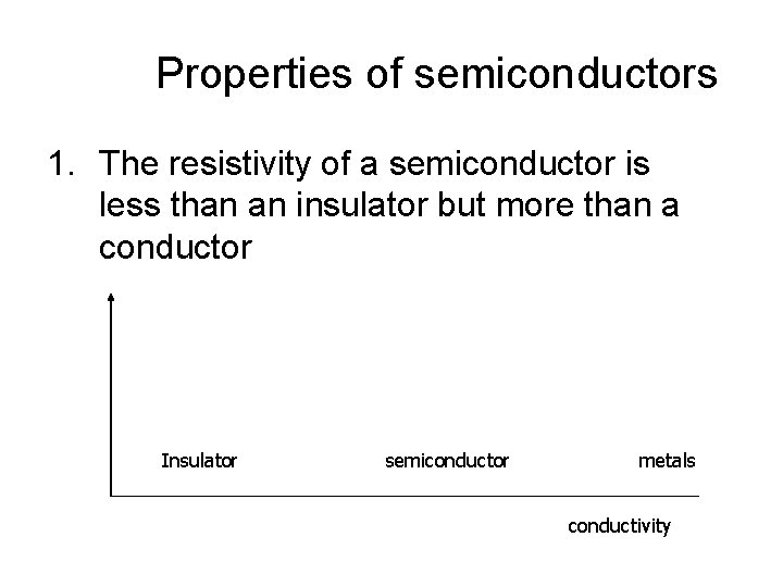
Properties of semiconductors 1. The resistivity of a semiconductor is less than an insulator but more than a conductor Insulator semiconductor metals conductivity

2. Semiconductors have –ve temperature coefficient of resistance. For example the resistance of semiconductor decreases with the increase in temperature. 3. When a suitable metallic impurity is added to semiconductor its current conducting property change.

Classification of semiconductors The semiconductors may be classified based on its constructure into: 1. Intrinsic semiconductors 2. Extrinsic semiconductors

1 - Intrinsic semiconductor • The semiconductor is pure. • At room temperature, electrons and holes are created due to thermal energy. • The conduction through the semiconductor is due to both electrons and holes. • The total current inside the semiconductor is the sum of currents due to free electrons and holes. • Example : Germanium and Silicon

2 - Extrinsic semiconductor • The conductivity of an intrinsic semiconductor can be increased by adding certain impurity atoms to the crystal. • The amount of impurity added extremely small, 1 atom of impurity for 10 e 6 intrinsic atom conduction through the semiconductor is due to both electrons and holes. • The total current inside the semiconductor is the sum of currents due to free electrons and holes. • Example : Germanium and Silicon

Depending upon the type of impurity atoms added, the extrinsic semiconductor can be classified into: 1 - N-type semiconductor 2 - P-type semiconductor

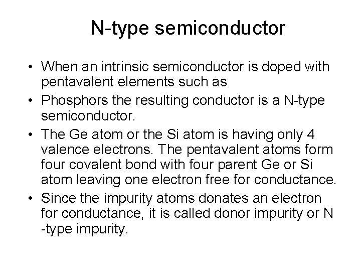
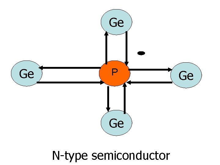
N-type semiconductor • When an intrinsic semiconductor is doped with pentavalent elements such as • Phosphors the resulting conductor is a N-type semiconductor. • The Ge atom or the Si atom is having only 4 valence electrons. The pentavalent atoms form four covalent bond with four parent Ge or Si atom leaving one electron free for conductance. • Since the impurity atoms donates an electron for conductance, it is called donor impurity or N -type impurity.

Ge Ge P Ge N-type semiconductor Ge

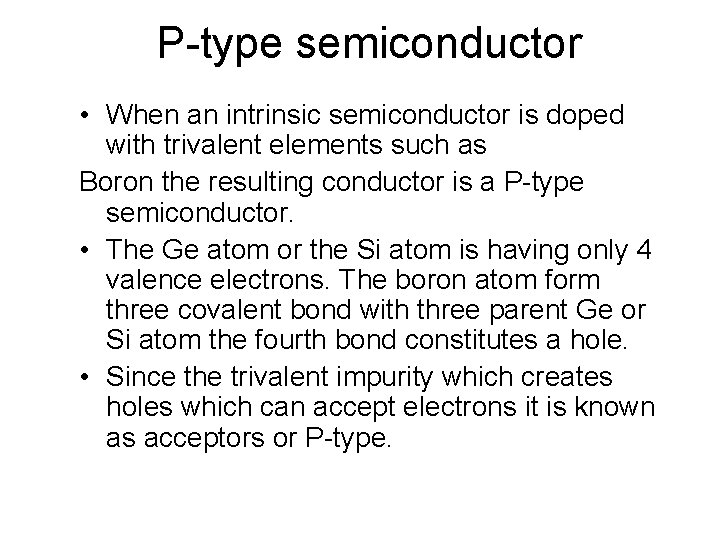
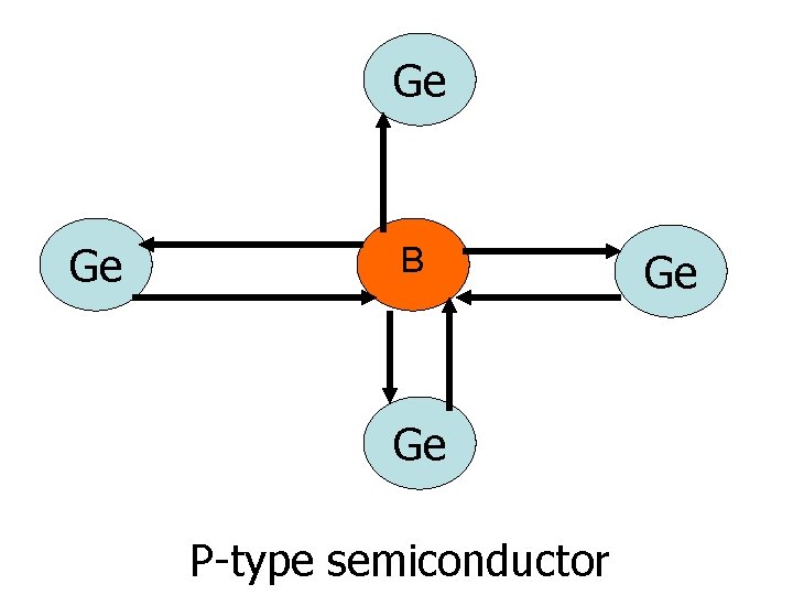
P-type semiconductor • When an intrinsic semiconductor is doped with trivalent elements such as Boron the resulting conductor is a P-type semiconductor. • The Ge atom or the Si atom is having only 4 valence electrons. The boron atom form three covalent bond with three parent Ge or Si atom the fourth bond constitutes a hole. • Since the trivalent impurity which creates holes which can accept electrons it is known as acceptors or P-type.

Ge Ge B Ge P-type semiconductor Ge

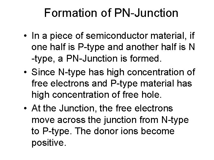
Formation of PN-Junction • In a piece of semiconductor material, if one half is P-type and another half is N -type, a PN-Junction is formed. • Since N-type has high concentration of free electrons and P-type material has high concentration of free hole. • At the Junction, the free electrons move across the junction from N-type to P-type. The donor ions become positive.

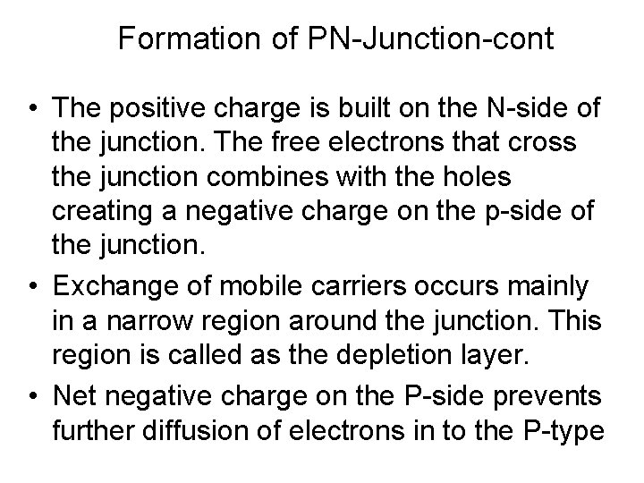
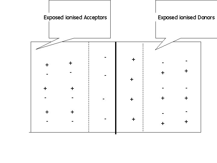
Formation of PN-Junction-cont • The positive charge is built on the N-side of the junction. The free electrons that cross the junction combines with the holes creating a negative charge on the p-side of the junction. • Exchange of mobile carriers occurs mainly in a narrow region around the junction. This region is called as the depletion layer. • Net negative charge on the P-side prevents further diffusion of electrons in to the P-type

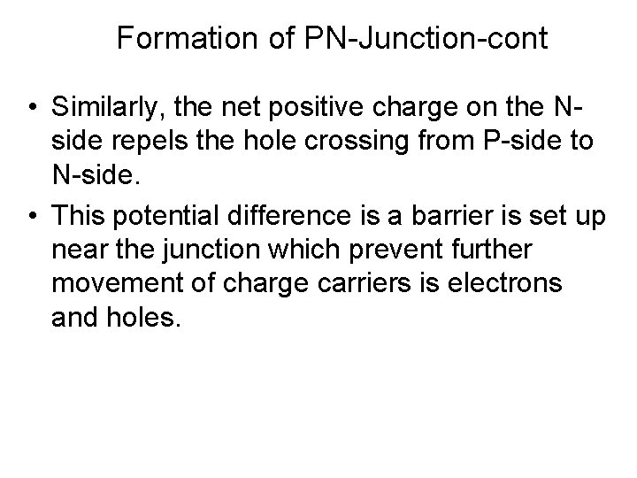
Formation of PN-Junction-cont • Similarly, the net positive charge on the Nside repels the hole crossing from P-side to N-side. • This potential difference is a barrier is set up near the junction which prevent further movement of charge carriers is electrons and holes.

Exposed ionised Acceptors + + - - Exposed ionised Donors + + - - + +

• The magnitude of the contact potential varies with doping levels and temperature. Its 0. 3 V for germanium and 0. 70 V for silicon