Electronics ELECTRICAL CONDUCTIVITY Materials are classified as l

- Slides: 40

Electronics

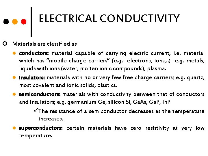
ELECTRICAL CONDUCTIVITY ¢ Materials are classified as l conductors: material capable of carrying electric current, i. e. material which has “mobile charge carriers” (e. g. electrons, ions, . . ) e. g. metals, liquids with ions (water, molten ionic compounds), plasma. l insulators: materials with no or very few free charge carriers; e. g. quartz, most covalent and ionic solids, plastics. l semiconductors: materials with conductivity between that of conductors and insulators; e. g. germanium Ge, silicon Si, Ga. As, Ga. P, In. P üThe resistance of a semiconductor decreases as the temperature increases. l superconductors: certain materials have zero resistivity at very low temperature.

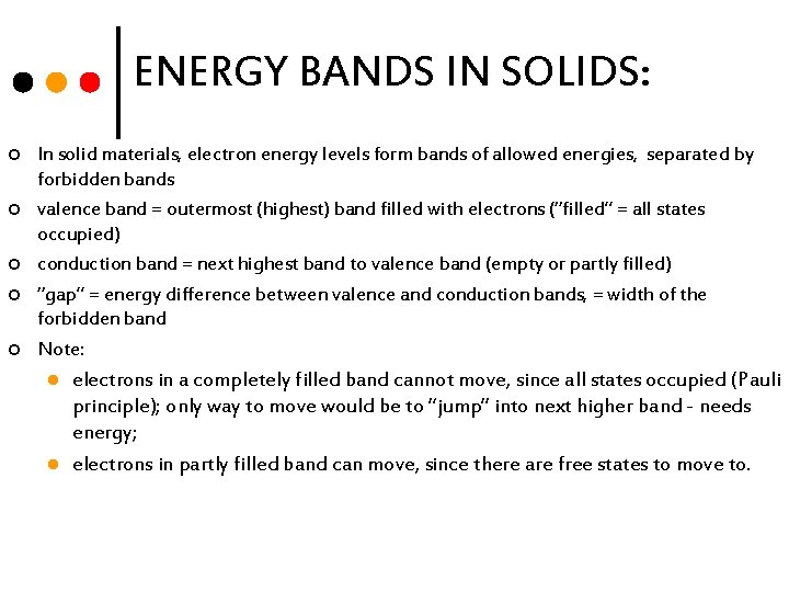
ENERGY BANDS IN SOLIDS: ¢ ¢ ¢ In solid materials, electron energy levels form bands of allowed energies, separated by forbidden bands valence band = outermost (highest) band filled with electrons (“filled” = all states occupied) conduction band = next highest band to valence band (empty or partly filled) “gap” = energy difference between valence and conduction bands, = width of the forbidden band Note: l l electrons in a completely filled band cannot move, since all states occupied (Pauli principle); only way to move would be to “jump” into next higher band - needs energy; electrons in partly filled band can move, since there are free states to move to.

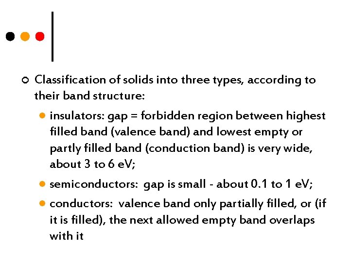
¢ Classification of solids into three types, according to their band structure: l insulators: gap = forbidden region between highest filled band (valence band) and lowest empty or partly filled band (conduction band) is very wide, about 3 to 6 e. V; l semiconductors: gap is small - about 0. 1 to 1 e. V; l conductors: valence band only partially filled, or (if it is filled), the next allowed empty band overlaps with it

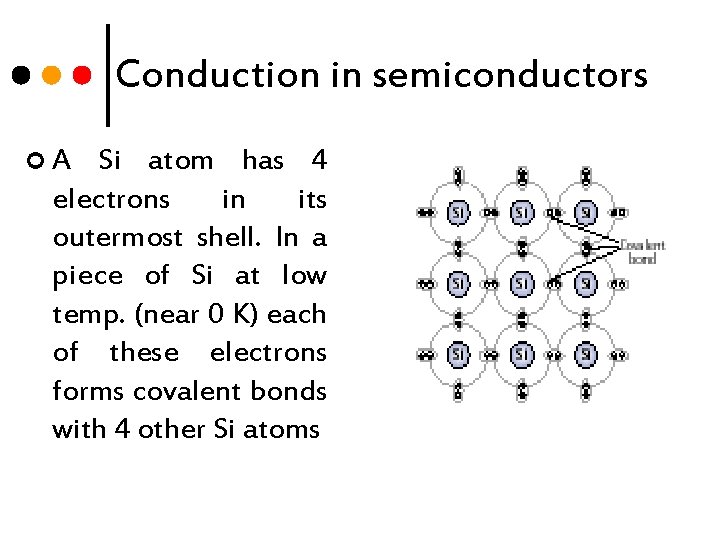
Conduction in semiconductors ¢A Si atom has 4 electrons in its outermost shell. In a piece of Si at low temp. (near 0 K) each of these electrons forms covalent bonds with 4 other Si atoms

¢ As the temp. of the semiconductor is increased, these electrons gain more energy. Some gain enough energy to break free of their bonds, and wander through the piece of material. ¢ Once an electron moves out of a bond, it leaves behind a ‘hole’ in that bond ¢ This hole is positive, and so can attract nearby electrons which then move out of their bond etc.

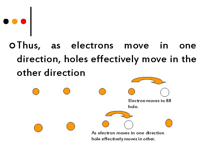
¢ Thus, as electrons move in one direction, holes effectively move in the other direction Electron moves to fill hole. As electron moves in one direction hole effectively moves in other.

¢ This is a difference between conduction in metals and semiconductors, in metals conduction is due solely to movement of electrons, in semiconductors it is due to movement of negative electrons and positive holes.

Intrinsic semiconductors ¢ When conduction in a semiconductor is due to electrons moving from - to + and an equal no. of holes moving from + to -, it is called intrinsic conduction ¢ The resistance of an intrinsic semiconductor, even at room temp. is quite high

Extrinsic semiconductors ¢ Are those with increased conduction due to the presence of impurity elements. ¢ It is important to note that even though there are extra FREE electrons or holes, the piece of material is still electrically neutral. Overall there are still the same TOTAL no. of electrons as protons

To increase conduction in a semiconductor ¢ (a) 3 ways Increase the temperature. As the temp. increases the no. of electrons which have enough energy to break free of their bonds increases, and so the conduction increases. A thermistor is a device whose resistance changes rapidly as the temperature changes

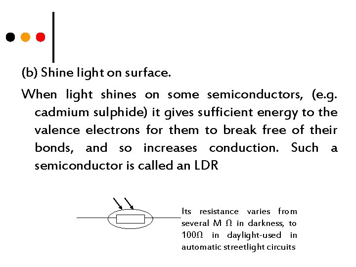
(b) Shine light on surface. When light shines on some semiconductors, (e. g. cadmium sulphide) it gives sufficient energy to the valence electrons for them to break free of their bonds, and so increases conduction. Such a semiconductor is called an LDR Its resistance varies from several M Ω in darkness, to 100Ω in daylight-used in automatic streetlight circuits

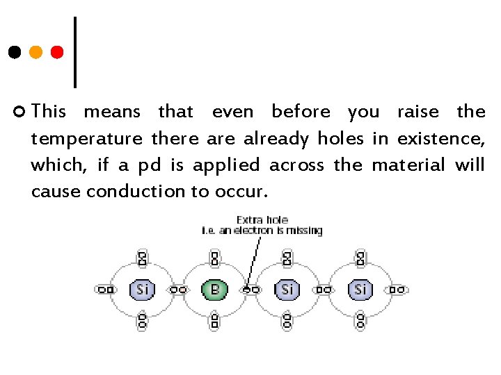
(c) Adding small amounts of impurities to the semiconductor can also effect its conduction. This process is known as doping Si has 4 valence electrons. B has 3 valence electrons. If a small amount of B is introduced into the Si lattice, at each location that a B atom occurs in the bond, there will be one electron missing, in other words, a positive hole exists.

¢ This means that even before you raise the temperature there already holes in existence, which, if a pd is applied across the material will cause conduction to occur.

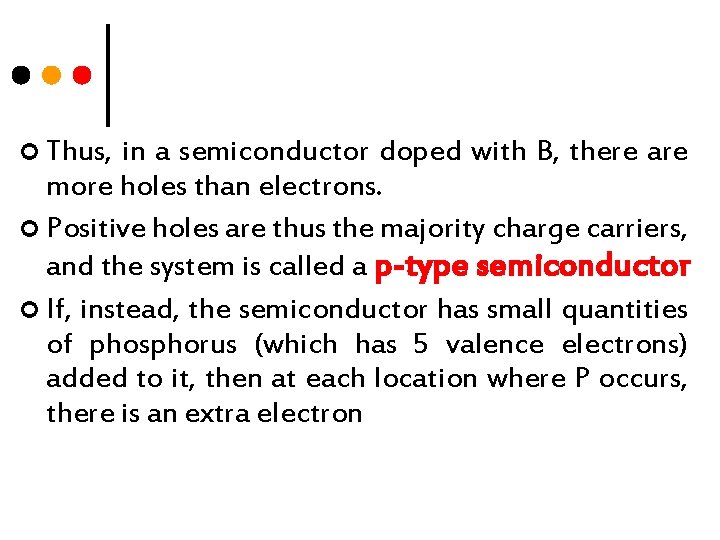
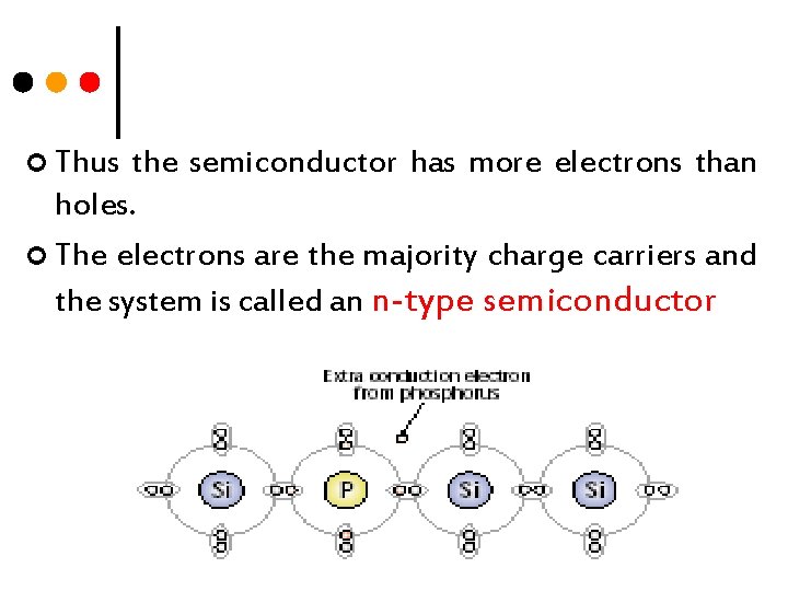
¢ Thus, in a semiconductor doped with B, there are more holes than electrons. ¢ Positive holes are thus the majority charge carriers, and the system is called a p-type semiconductor ¢ If, instead, the semiconductor has small quantities of phosphorus (which has 5 valence electrons) added to it, then at each location where P occurs, there is an extra electron

¢ Thus the semiconductor has more electrons than holes. ¢ The electrons are the majority charge carriers and the system is called an n-type semiconductor

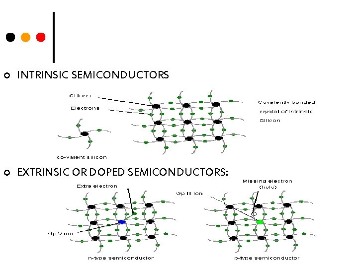
¢ INTRINSIC SEMICONDUCTORS ¢ EXTRINSIC OR DOPED SEMICONDUCTORS:

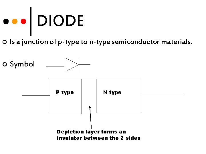
DIODE ¢ Is a junction of p-type to n-type semiconductor materials. ¢ Symbol P type N type Depletion layer forms an insulator between the 2 sides

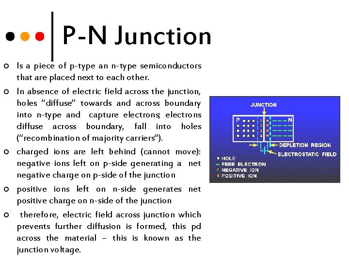
P-N Junction ¢ ¢ ¢ Is a piece of p-type an n-type semiconductors that are placed next to each other. In absence of electric field across the junction, holes “diffuse” towards and across boundary into n-type and capture electrons; electrons diffuse across boundary, fall into holes (“recombination of majority carriers”). charged ions are left behind (cannot move): negative ions left on p-side generating a net negative charge on p-side of the junction positive ions left on n-side generates net positive charge on n-side of the junction therefore, electric field across junction which prevents further diffusion is formed, this pd across the material – this is known as the junction voltage.

Depletion layer ¢ ¢ Also, at the boundary region (junction) there are no free electrons and no holes (as they have cancelled each other) Thus, in this region there are no free charge carriers, so no conduction can occur. This insulating layer is called the depletion layer. In order to get current to flow through the diode it is necessary to break down the depletion layer, which have the so called junction voltage (i. e. drive free electrons and free holes into the layer).

Reverse biased pn junction ¢ If the + of a battery is connected to the n -type and the – terminal to the p-type, the free electrons and free holes are attracted back towards the battery. ¢ Hence the depletion layer grows. Thus a reverse biased pn junction does not conduct current.

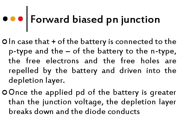
Forward biased pn junction ¢ In case that + of the battery is connected to the p-type and the – of the battery to the n-type, the free electrons and the free holes are repelled by the battery and driven into the depletion layer. ¢ Once the applied pd of the battery is greater than the junction voltage, the depletion layer breaks down and the diode conducts

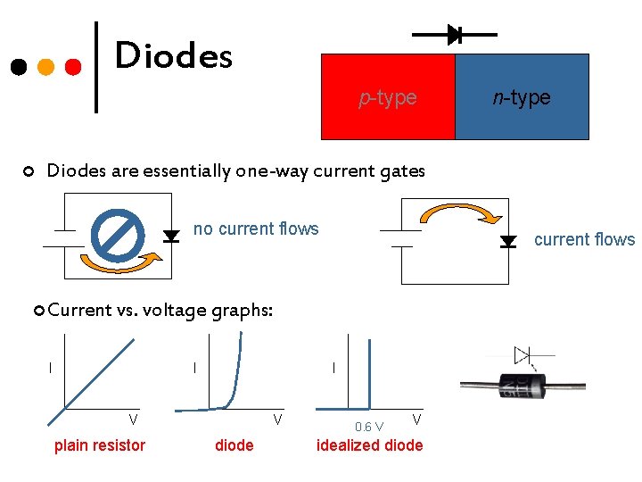
Diodes p-type ¢ n-type Diodes are essentially one-way current gates no current flows ¢Current vs. voltage graphs: I I I V plain resistor V diode 0. 6 V V idealized diode

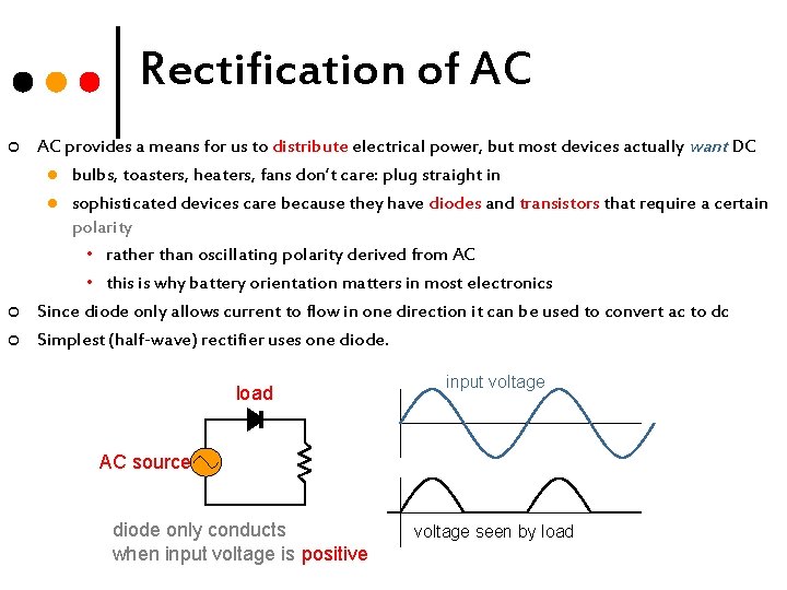
Rectification of AC ¢ ¢ ¢ AC provides a means for us to distribute electrical power, but most devices actually want DC l bulbs, toasters, heaters, fans don’t care: plug straight in l sophisticated devices care because they have diodes and transistors that require a certain polarity • rather than oscillating polarity derived from AC • this is why battery orientation matters in most electronics Since diode only allows current to flow in one direction it can be used to convert ac to dc Simplest (half-wave) rectifier uses one diode. load input voltage AC source diode only conducts when input voltage is positive voltage seen by load

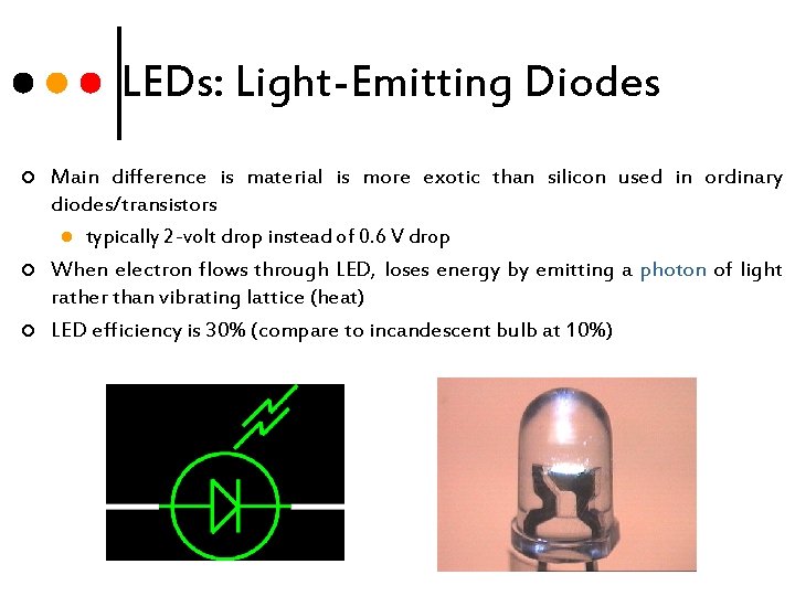
LEDs: Light-Emitting Diodes ¢ ¢ ¢ Main difference is material is more exotic than silicon used in ordinary diodes/transistors l typically 2 -volt drop instead of 0. 6 V drop When electron flows through LED, loses energy by emitting a photon of light rather than vibrating lattice (heat) LED efficiency is 30% (compare to incandescent bulb at 10%)

Transistors A Transistor is an especial arrangement of semiconductor materials. Nowadays are fundamental components in almost all electronic devices. Transistors are often said to be the most significant invention of the 20 th Century.

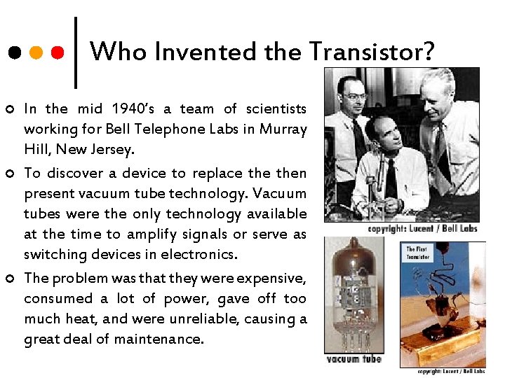
Who Invented the Transistor? ¢ ¢ ¢ In the mid 1940’s a team of scientists working for Bell Telephone Labs in Murray Hill, New Jersey. To discover a device to replace then present vacuum tube technology. Vacuum tubes were the only technology available at the time to amplify signals or serve as switching devices in electronics. The problem was that they were expensive, consumed a lot of power, gave off too much heat, and were unreliable, causing a great deal of maintenance.

Who Invented the Transistor? ¢ The scientists that were responsible for the 1947 invention of the transistor were: John Bardeen, Walter Brattain, and William Shockley. Bardeen, with a Ph. D. in mathematics and physics from Princeton University, was a specialist in the electron conducting properties of semiconductors. Brattain, Ph. D. , was an expert in the nature of the atomic structure of solids at their surface level and solid-state physics. Shockley, Ph. D. , was the director of transistor research for Bell Labs. Their original patent name for the transistor was: “Semiconductor amplifier; Three-electrode circuit element utilizing semiconductive materials. ” In 1956, the group was awarded the Noble Prize in Physics for their invention of the transistor. In 1977, John Bardeen was awarded the Presidential Medal of Freedom.

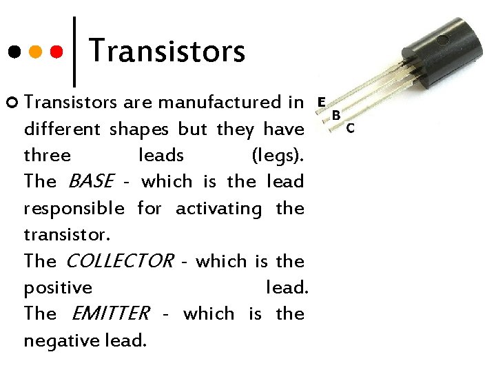
Transistors ¢ Transistors are manufactured in different shapes but they have three leads (legs). The BASE - which is the lead responsible for activating the transistor. The COLLECTOR - which is the positive lead. The EMITTER - which is the negative lead.

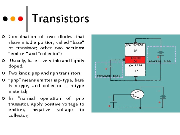
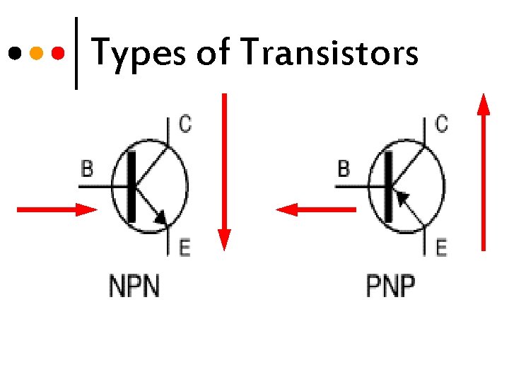
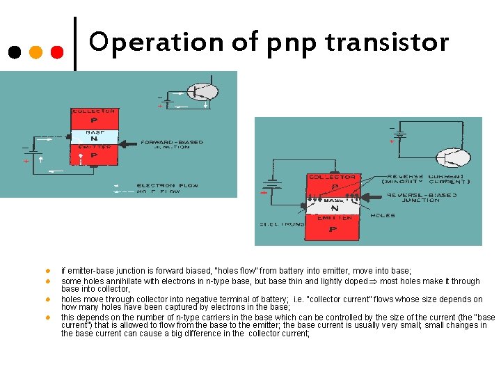
Transistors ¢ ¢ ¢ Combination of two diodes that share middle portion, called “base” of transistor; other two sections: “emitter'' and “collector”; Usually, base is very thin and lightly doped. Two kinds: pnp and npn transistors “pnp” means emitter is p-type, base is n-type, and collector is p-type material; In “normal operation of pnp transistor, apply positive voltage to emitter, negative voltage to collector;

Types of Transistors

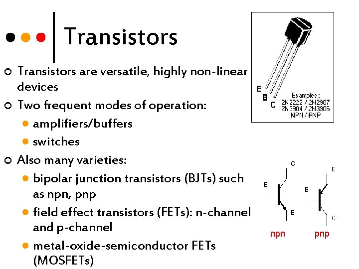
Transistors ¢ ¢ ¢ Transistors are versatile, highly non-linear devices Two frequent modes of operation: l amplifiers/buffers l switches Also many varieties: l bipolar junction transistors (BJTs) such as npn, pnp l field effect transistors (FETs): n-channel and p-channel l metal-oxide-semiconductor FETs (MOSFETs) C B E npn C pnp

Function of Transistors ¢ ¢ ¢ They controls large electrical output signal with changes to a small input signal. This is analogous to the small amount of effort required to open a tap (faucet) to release a large flow of water. Since a large amount of current can be controlled by a small amount of current, a transistor acts as an amplifier. A transistor acts as a switch which can open and close many times per second. The amount of current amplification is called the current gain, symbol h. FE

Operation of pnp transistor l l if emitter-base junction is forward biased, “holes flow” from battery into emitter, move into base; some holes annihilate with electrons in n-type base, but base thin and lightly doped most holes make it through base into collector, holes move through collector into negative terminal of battery; i. e. “collector current” flows whose size depends on how many holes have been captured by electrons in the base; this depends on the number of n-type carriers in the base which can be controlled by the size of the current (the “base current”) that is allowed to flow from the base to the emitter; the base current is usually very small; small changes in the base current can cause a big difference in the collector current;

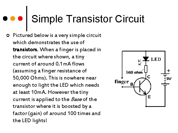
Simple Transistor Circuit ¢ Pictured below is a very simple circuit which demonstrates the use of transistors. When a finger is placed in the circuit where shown, a tiny current of around 0. 1 m. A flows (assuming a finger resistance of 50, 000 Ohms). This is nowhere near enough to light the LED which needs at least 10 m. A. However the tiny current is applied to the Base of the transistor where it is boosted by a factor (gain) of around 100 times and the LED lights!

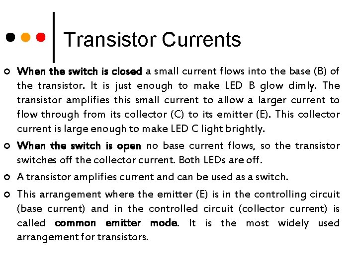
Transistor Currents ¢ ¢ When the switch is closed a small current flows into the base (B) of the transistor. It is just enough to make LED B glow dimly. The transistor amplifies this small current to allow a larger current to flow through from its collector (C) to its emitter (E). This collector current is large enough to make LED C light brightly. When the switch is open no base current flows, so the transistor switches off the collector current. Both LEDs are off. A transistor amplifies current and can be used as a switch. This arrangement where the emitter (E) is in the controlling circuit (base current) and in the controlled circuit (collector current) is called common emitter mode. It is the most widely used arrangement for transistors.

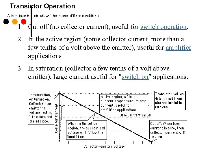
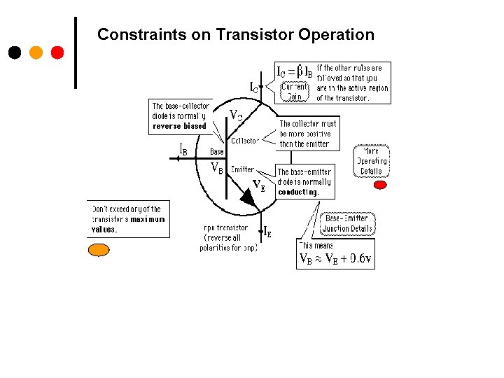
Transistor Operation A transistor in a circuit will be in one of three conditions 1. Cut off (no collector current), useful for switch operation. 2. In the active region (some collector current, more than a few tenths of a volt above the emitter), useful for amplifier applications 3. In saturation (collector a few tenths of a volt above emitter), large current useful for "switch on" applications.

Constraints on Transistor Operation

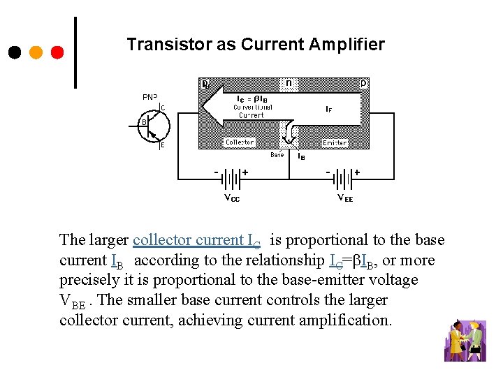
Transistor as Current Amplifier The larger collector current IC is proportional to the base current IB according to the relationship IC= IB, or more precisely it is proportional to the base-emitter voltage VBE. The smaller base current controls the larger collector current, achieving current amplification.

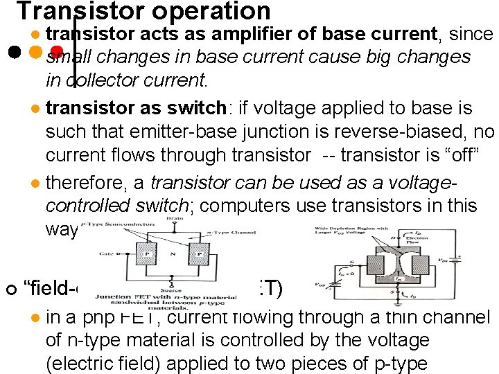
Transistor operation transistor acts as amplifier of base current, since small changes in base current cause big changes in collector current. l transistor as switch: if voltage applied to base is such that emitter-base junction is reverse-biased, no current flows through transistor -- transistor is “off” l therefore, a transistor can be used as a voltagecontrolled switch; computers use transistors in this way. l ¢ “field-effect transistor” (FET) l in a pnp FET, current flowing through a thin channel of n-type material is controlled by the voltage (electric field) applied to two pieces of p-type