Electronics 1 Lecture 2 Ahsan Khawaja ahsankhawajacomsats edu
- Slides: 36

Electronics 1 Lecture 2 Ahsan Khawaja ahsan_khawaja@comsats. edu. pk Lecturer Room 102 Department of Electrical Engineering

Electronic Materials • • The goal of electronic materials is to generate and control the flow of an electric current. Electronic materials include: 1. Conductors: have low resistance which allows electric current flow 2. Insulators: have high resistance which suppresses electric current flow 3. Semiconductors: can allow or suppress electrical current flow

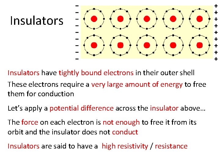
Insulators have tightly bound electrons in their outer shell These electrons require a very large amount of energy to free them for conduction Let’s apply a potential difference across the insulator above… The force on each electron is not enough to free it from its orbit and the insulator does not conduct Insulators are said to have a high resistivity / resistance

Insulators • Insulators have a high resistance so current does not flow in them. • Good insulators include: – Glass, ceramic, plastics, & wood • Most insulators are compounds of several elements. • The atoms are tightly bound to one another so electrons are difficult to strip away for current flow.

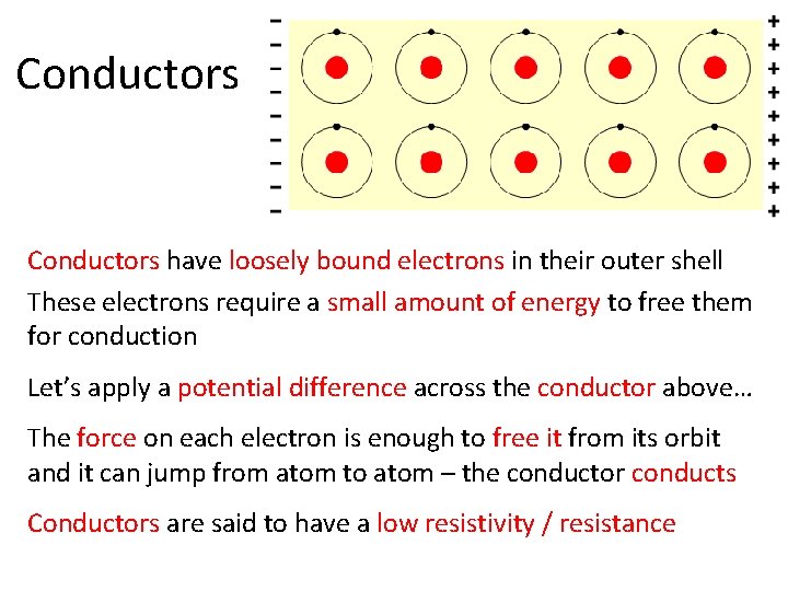
Conductors have loosely bound electrons in their outer shell These electrons require a small amount of energy to free them for conduction Let’s apply a potential difference across the conductor above… The force on each electron is enough to free it from its orbit and it can jump from atom to atom – the conductor conducts Conductors are said to have a low resistivity / resistance

Conductors • Good conductors have low resistance so electrons flow through them with ease. • Best element conductors include: – Copper, silver, gold, aluminum, & nickel • Alloys are also good conductors: – Brass & steel • Good conductors can also be liquid: – Salt water

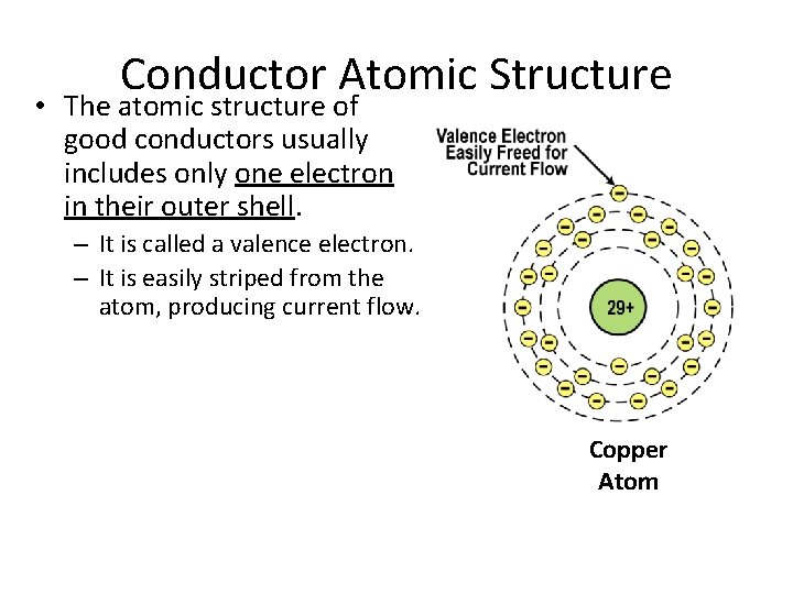
Conductor Atomic Structure • The atomic structure of good conductors usually includes only one electron in their outer shell. – It is called a valence electron. – It is easily striped from the atom, producing current flow. Copper Atom

Semiconductors • A material whose properties are such that it is not quite a conductor, not quite an insulator. • Semiconductors have a resistivity/resistance between that of conductors and insulators. • Their electrons are not free to move but a little energy will free them for conduction • Some common semiconductors – elemental • Si - Silicon (most common) • Ge - Germanium – compound • • • Ga. As - Gallium arsenide Ga. P - Gallium phosphide Al. As - Aluminum arsenide Al. P - Aluminum phosphide In. P - Indium Phosphide (The resistance of a semiconductor decreases as the temperature increases. )

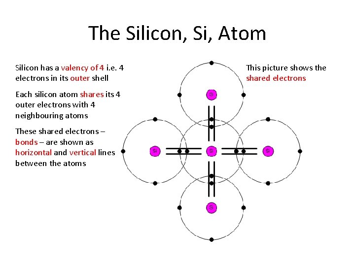
The Silicon, Si, Atom Silicon has a valency of 4 i. e. 4 electrons in its outer shell Each silicon atom shares its 4 outer electrons with 4 neighbouring atoms These shared electrons – bonds – are shown as horizontal and vertical lines between the atoms This picture shows the shared electrons

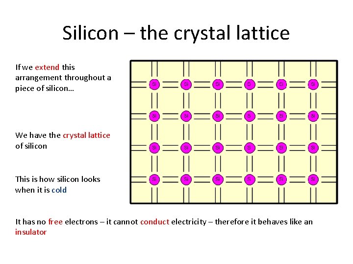
Silicon – the crystal lattice If we extend this arrangement throughout a piece of silicon… We have the crystal lattice of silicon This is how silicon looks when it is cold It has no free electrons – it cannot conduct electricity – therefore it behaves like an insulator

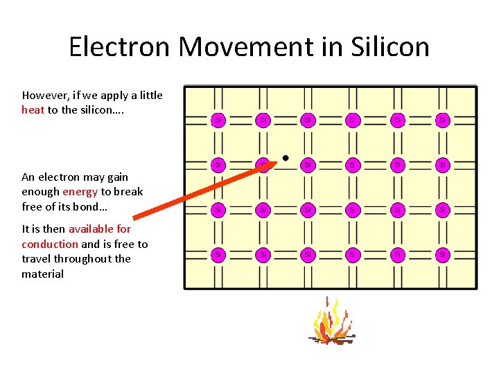
Electron Movement in Silicon However, if we apply a little heat to the silicon…. An electron may gain enough energy to break free of its bond… It is then available for conduction and is free to travel throughout the material

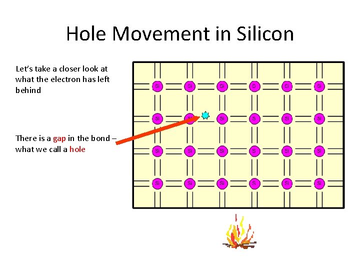
Hole Movement in Silicon Let’s take a closer look at what the electron has left behind There is a gap in the bond – what we call a hole

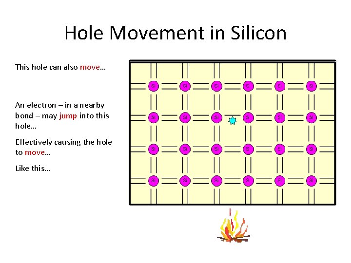
Hole Movement in Silicon This hole can also move… An electron – in a nearby bond – may jump into this hole… Effectively causing the hole to move… Like this…

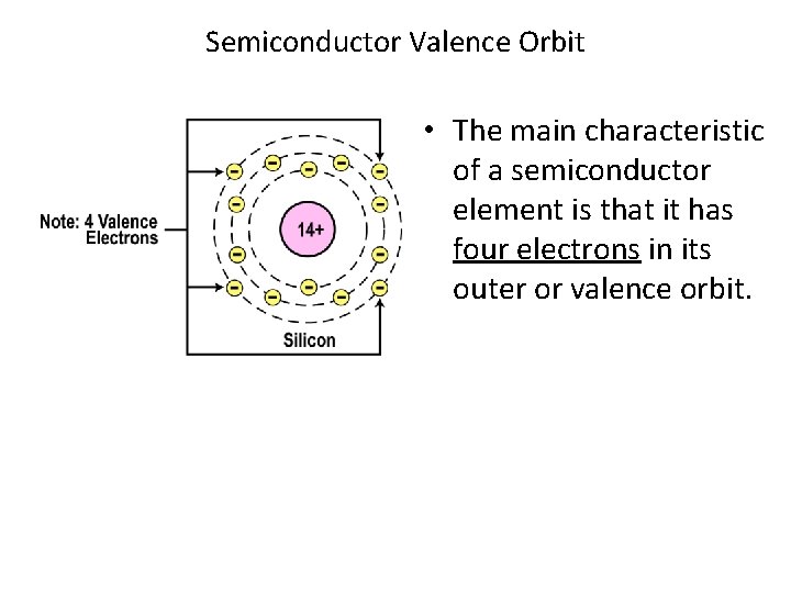
Semiconductor Valence Orbit • The main characteristic of a semiconductor element is that it has four electrons in its outer or valence orbit.

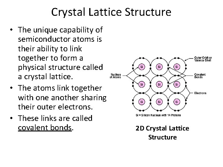
Crystal Lattice Structure • The unique capability of semiconductor atoms is their ability to link together to form a physical structure called a crystal lattice. • The atoms link together with one another sharing their outer electrons. • These links are called covalent bonds. 2 D Crystal Lattice Structure

Semiconductors • An intrinsic semiconductor, also called an undoped semiconductor or i-type semiconductor, is a pure semiconductor without any significant dopant species present. • An extrinsic semiconductor is a semiconductor that has been doped.

Doping • Relying on heat or light for conduction does not make for reliable electronics • To make the semiconductor conduct electricity, other atoms called impurities must be added. • “Impurities” are different elements. • This process is called doping.

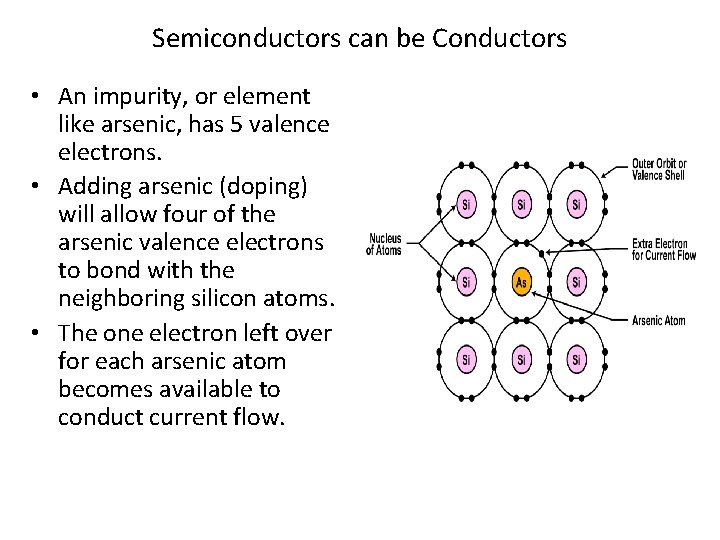
Semiconductors can be Conductors • An impurity, or element like arsenic, has 5 valence electrons. • Adding arsenic (doping) will allow four of the arsenic valence electrons to bond with the neighboring silicon atoms. • The one electron left over for each arsenic atom becomes available to conduct current flow.

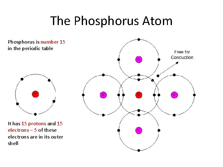
The Phosphorus Atom Phosphorus is number 15 in the periodic table It has 15 protons and 15 electrons – 5 of these electrons are in its outer shell

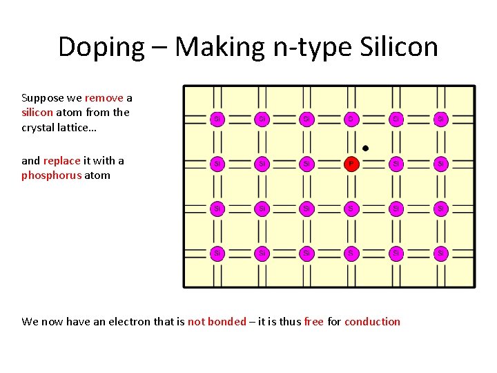
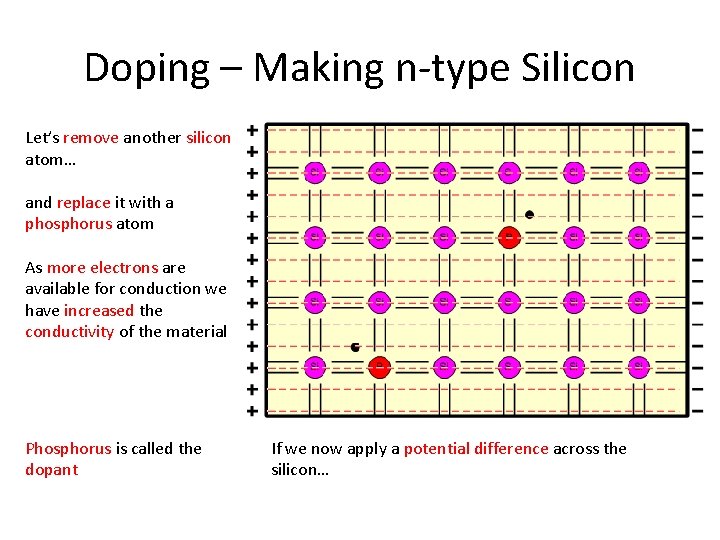
Doping – Making n-type Silicon Suppose we remove a silicon atom from the crystal lattice… and replace it with a phosphorus atom We now have an electron that is not bonded – it is thus free for conduction

Doping – Making n-type Silicon Let’s remove another silicon atom… and replace it with a phosphorus atom As more electrons are available for conduction we have increased the conductivity of the material Phosphorus is called the dopant If we now apply a potential difference across the silicon…

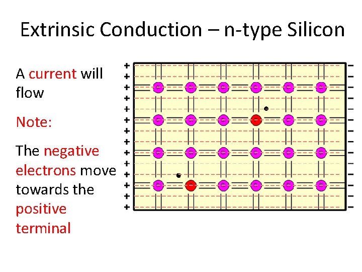
Extrinsic Conduction – n-type Silicon A current will flow Note: The negative electrons move towards the positive terminal

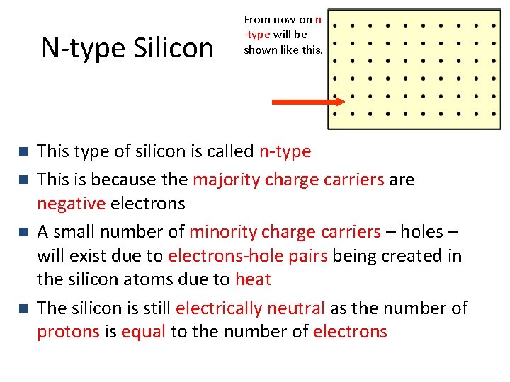
N-type Silicon n n From now on n -type will be shown like this. This type of silicon is called n-type This is because the majority charge carriers are negative electrons A small number of minority charge carriers – holes – will exist due to electrons-hole pairs being created in the silicon atoms due to heat The silicon is still electrically neutral as the number of protons is equal to the number of electrons

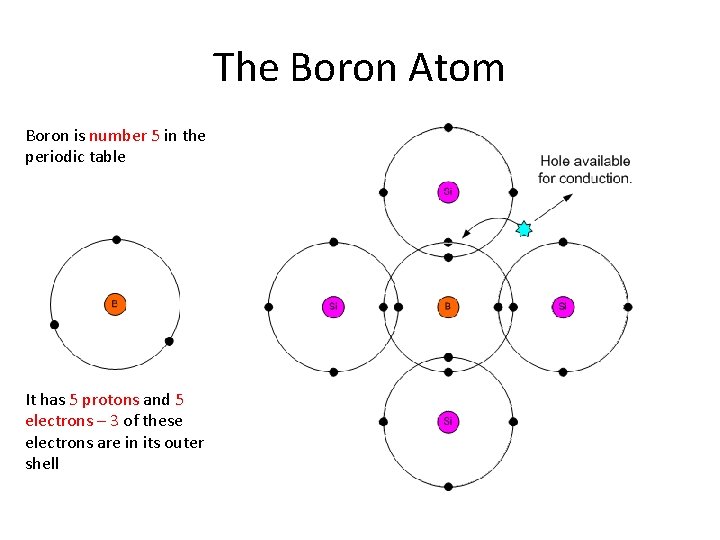
The Boron Atom Boron is number 5 in the periodic table It has 5 protons and 5 electrons – 3 of these electrons are in its outer shell

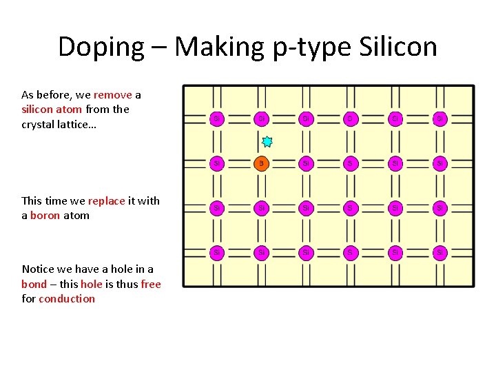
Doping – Making p-type Silicon As before, we remove a silicon atom from the crystal lattice… This time we replace it with a boron atom Notice we have a hole in a bond – this hole is thus free for conduction

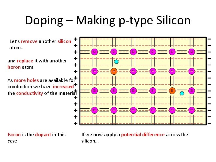
Doping – Making p-type Silicon Let’s remove another silicon atom… and replace it with another boron atom As more holes are available for conduction we have increased the conductivity of the material Boron is the dopant in this case If we now apply a potential difference across the silicon…

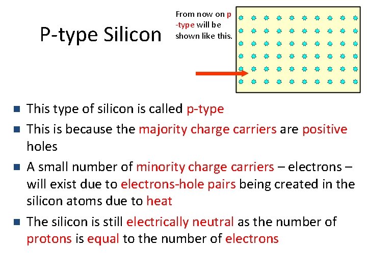
P-type Silicon n n From now on p -type will be shown like this. This type of silicon is called p-type This is because the majority charge carriers are positive holes A small number of minority charge carriers – electrons – will exist due to electrons-hole pairs being created in the silicon atoms due to heat The silicon is still electrically neutral as the number of protons is equal to the number of electrons

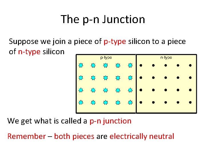
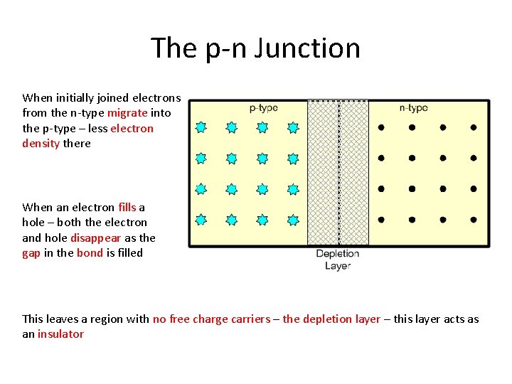
The p-n Junction Suppose we join a piece of p-type silicon to a piece of n-type silicon We get what is called a p-n junction Remember – both pieces are electrically neutral

The p-n Junction When initially joined electrons from the n-type migrate into the p-type – less electron density there When an electron fills a hole – both the electron and hole disappear as the gap in the bond is filled This leaves a region with no free charge carriers – the depletion layer – this layer acts as an insulator

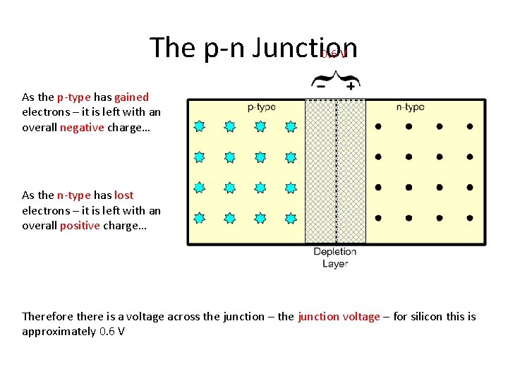
The p-n Junction 0. 6 V As the p-type has gained electrons – it is left with an overall negative charge… As the n-type has lost electrons – it is left with an overall positive charge… Therefore there is a voltage across the junction – the junction voltage – for silicon this is approximately 0. 6 V

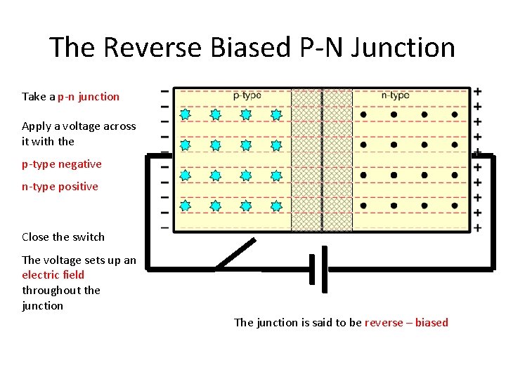
The Reverse Biased P-N Junction Take a p-n junction Apply a voltage across it with the p-type negative n-type positive Close the switch The voltage sets up an electric field throughout the junction The junction is said to be reverse – biased

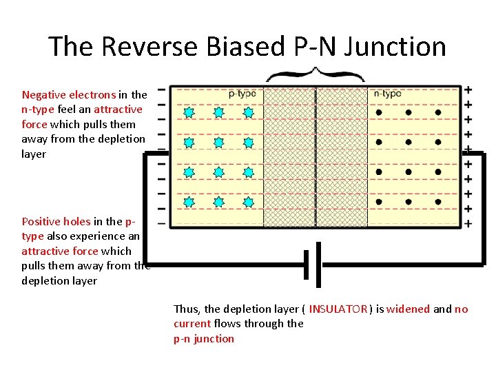
The Reverse Biased P-N Junction Negative electrons in the n-type feel an attractive force which pulls them away from the depletion layer Positive holes in the ptype also experience an attractive force which pulls them away from the depletion layer Thus, the depletion layer ( INSULATOR ) is widened and no current flows through the p-n junction

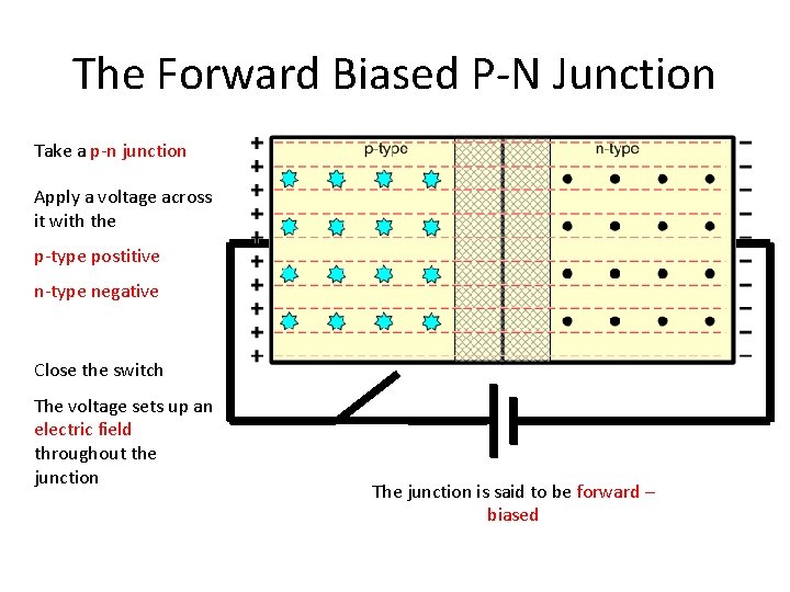
The Forward Biased P-N Junction Take a p-n junction Apply a voltage across it with the p-type postitive n-type negative Close the switch The voltage sets up an electric field throughout the junction The junction is said to be forward – biased

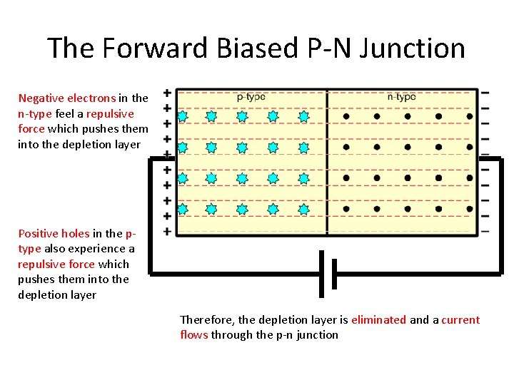
The Forward Biased P-N Junction Negative electrons in the n-type feel a repulsive force which pushes them into the depletion layer Positive holes in the ptype also experience a repulsive force which pushes them into the depletion layer Therefore, the depletion layer is eliminated and a current flows through the p-n junction

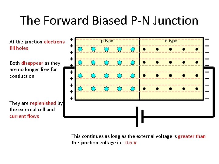
The Forward Biased P-N Junction At the junction electrons fill holes Both disappear as they are no longer free for conduction They are replenished by the external cell and current flows This continues as long as the external voltage is greater than the junction voltage i. e. 0. 6 V

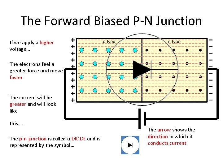
The Forward Biased P-N Junction If we apply a higher voltage… The electrons feel a greater force and move faster The current will be greater and will look like this…. The p-n junction is called a DIODE and is represented by the symbol… The arrow shows the direction in which it conducts current