Electronic Design Automation Course Outline 1 Digital circuit
- Slides: 24

Electronic Design Automation

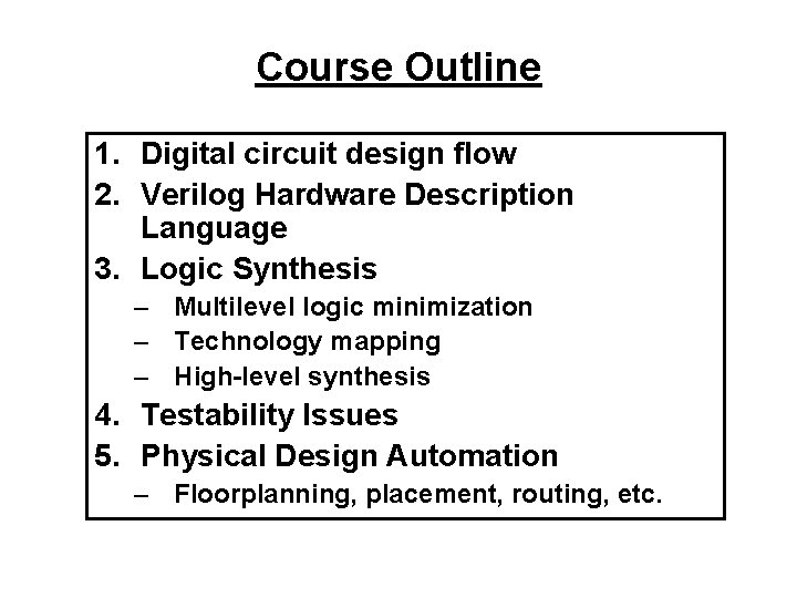
Course Outline 1. Digital circuit design flow 2. Verilog Hardware Description Language 3. Logic Synthesis – Multilevel logic minimization – Technology mapping – High-level synthesis 4. Testability Issues 5. Physical Design Automation – Floorplanning, placement, routing, etc.

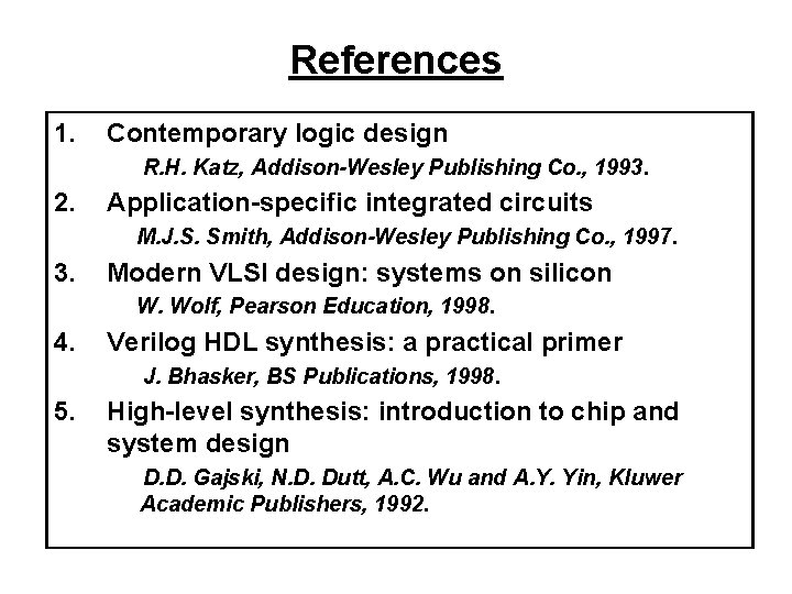
References 1. Contemporary logic design R. H. Katz, Addison-Wesley Publishing Co. , 1993. 2. Application-specific integrated circuits M. J. S. Smith, Addison-Wesley Publishing Co. , 1997. 3. Modern VLSI design: systems on silicon W. Wolf, Pearson Education, 1998. 4. Verilog HDL synthesis: a practical primer J. Bhasker, BS Publications, 1998. 5. High-level synthesis: introduction to chip and system design D. D. Gajski, N. D. Dutt, A. C. Wu and A. Y. Yin, Kluwer Academic Publishers, 1992.

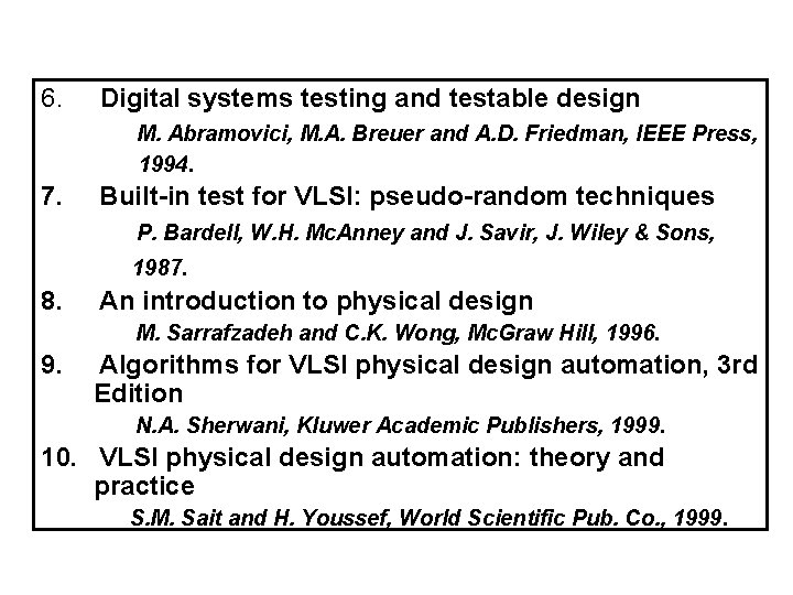
6. Digital systems testing and testable design M. Abramovici, M. A. Breuer and A. D. Friedman, IEEE Press, 1994. 7. Built-in test for VLSI: pseudo-random techniques P. Bardell, W. H. Mc. Anney and J. Savir, J. Wiley & Sons, 1987. 8. An introduction to physical design M. Sarrafzadeh and C. K. Wong, Mc. Graw Hill, 1996. 9. Algorithms for VLSI physical design automation, 3 rd Edition N. A. Sherwani, Kluwer Academic Publishers, 1999. 10. VLSI physical design automation: theory and practice S. M. Sait and H. Youssef, World Scientific Pub. Co. , 1999.

Digital Circuit Design Flow

Digital Design Process • Design complexity increasing rapidly – Increased size and complexity – CAD tools are essential • The present trend – Standardize the design flow

What is design flow? • Standardized design procedure – Starting from the design idea down to the actual implementation • Encompasses many steps – Specification – Synthesis – Simulation – Layout – Testability analysis – Many more ……

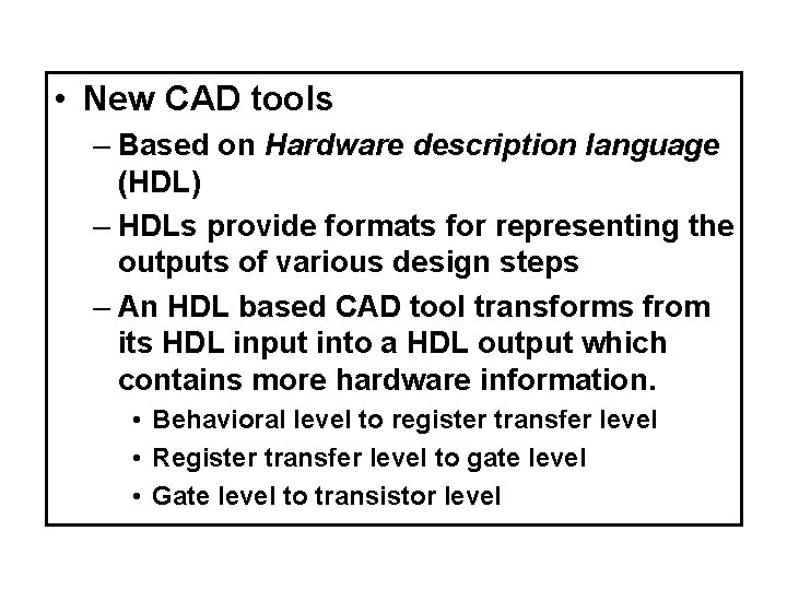
• New CAD tools – Based on Hardware description language (HDL) – HDLs provide formats for representing the outputs of various design steps – An HDL based CAD tool transforms from its HDL input into a HDL output which contains more hardware information. • Behavioral level to register transfer level • Register transfer level to gate level • Gate level to transistor level

Two Competing HDLs 1. Verilog 2. VHDL In this course we would be concentrating on Verilog only

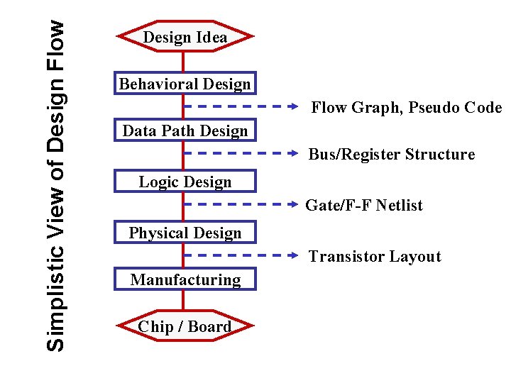
Simplistic View of Design Flow Design Idea Behavioral Design Flow Graph, Pseudo Code Data Path Design Bus/Register Structure Logic Design Gate/F-F Netlist Physical Design Transistor Layout Manufacturing Chip / Board

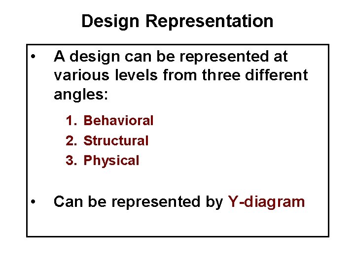
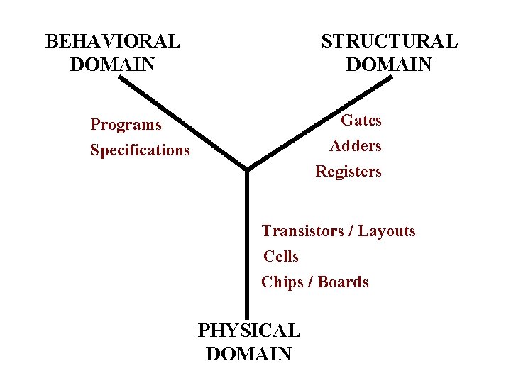
Design Representation • A design can be represented at various levels from three different angles: 1. Behavioral 2. Structural 3. Physical • Can be represented by Y-diagram

BEHAVIORAL DOMAIN STRUCTURAL DOMAIN Gates Programs Adders Registers Specifications Transistors / Layouts Cells Chips / Boards PHYSICAL DOMAIN

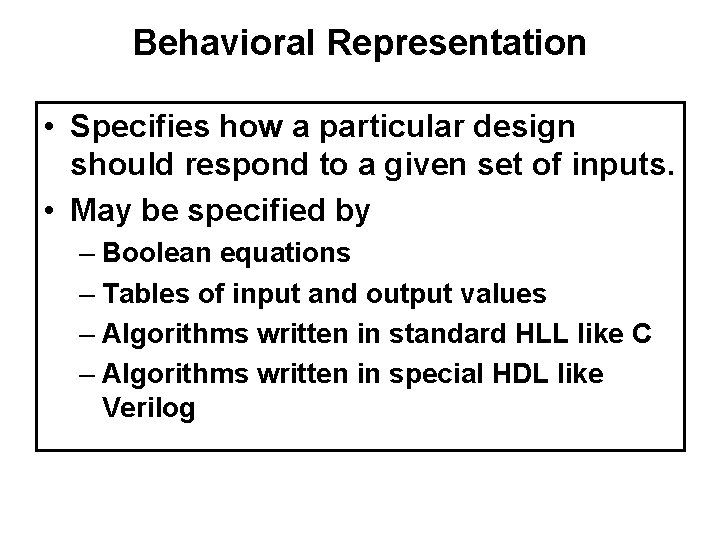
Behavioral Representation • Specifies how a particular design should respond to a given set of inputs. • May be specified by – Boolean equations – Tables of input and output values – Algorithms written in standard HLL like C – Algorithms written in special HDL like Verilog

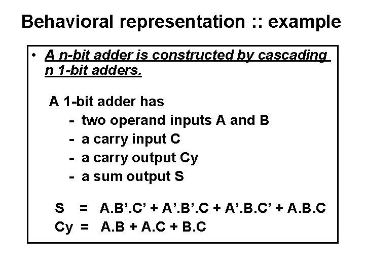
Behavioral representation : : example • A n-bit adder is constructed by cascading n 1 -bit adders. A 1 -bit adder has - two operand inputs A and B - a carry input C - a carry output Cy - a sum output S S = A. B’. C’ + A’. B’. C + A’. B. C’ + A. B. C Cy = A. B + A. C + B. C

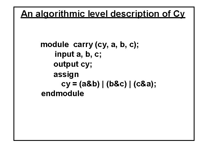
An algorithmic level description of Cy module carry (cy, a, b, c); input a, b, c; output cy; assign cy = (a&b) | (b&c) | (c&a); endmodule

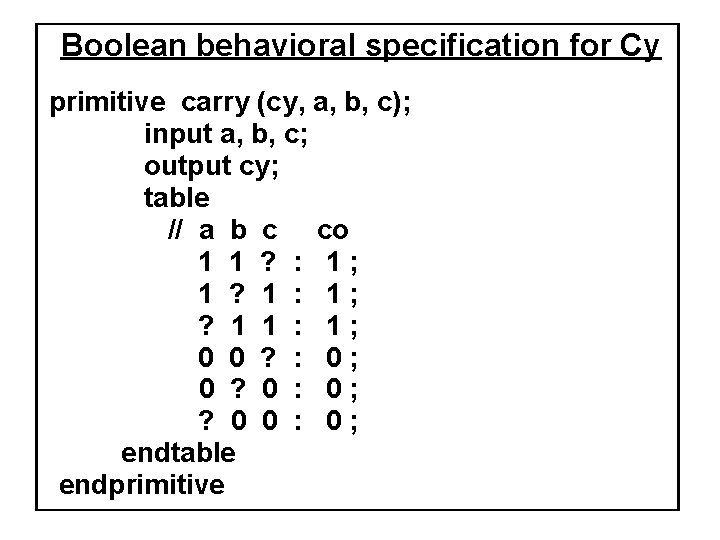
Boolean behavioral specification for Cy primitive carry (cy, a, b, c); input a, b, c; output cy; table // a b c co 1 1 ? : 1; 1 ? 1 : 1; ? 1 1 : 1; 0 0 ? : 0; 0 ? 0 : 0; ? 0 0 : 0; endtable endprimitive

Structural Representation • Specifies how components are interconnected. • In general, the description is a list of modules and their interconnects. – called netlist. – can be specified at various levels.

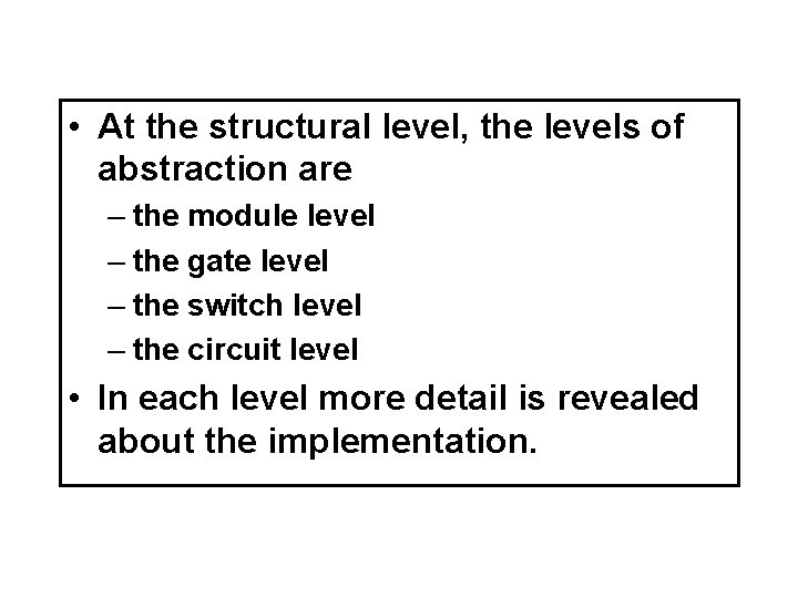
• At the structural level, the levels of abstraction are – the module level – the gate level – the switch level – the circuit level • In each level more detail is revealed about the implementation.

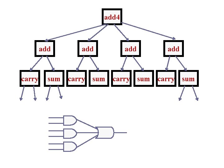
add 4 add carry add add sum carry sum

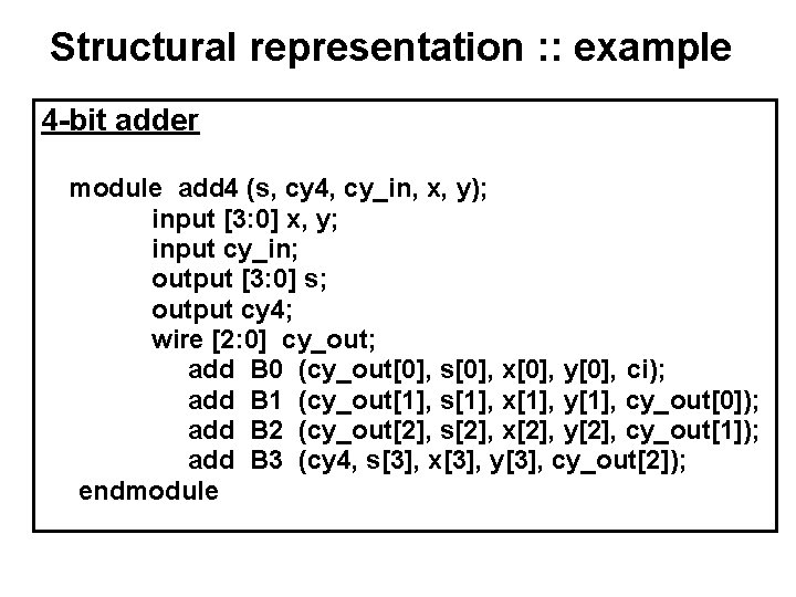
Structural representation : : example 4 -bit adder module add 4 (s, cy 4, cy_in, x, y); input [3: 0] x, y; input cy_in; output [3: 0] s; output cy 4; wire [2: 0] cy_out; add B 0 (cy_out[0], s[0], x[0], y[0], ci); add B 1 (cy_out[1], s[1], x[1], y[1], cy_out[0]); add B 2 (cy_out[2], s[2], x[2], y[2], cy_out[1]); add B 3 (cy 4, s[3], x[3], y[3], cy_out[2]); endmodule

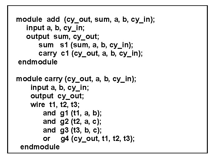
module add (cy_out, sum, a, b, cy_in); input a, b, cy_in; output sum, cy_out; sum s 1 (sum, a, b, cy_in); carry c 1 (cy_out, a, b, cy_in); endmodule carry (cy_out, a, b, cy_in); input a, b, cy_in; output cy_out; wire t 1, t 2, t 3; and g 1 (t 1, a, b); and g 2 (t 2, a, c); and g 3 (t 3, b, c); or g 4 (cy_out, t 1, t 2, t 3); endmodule

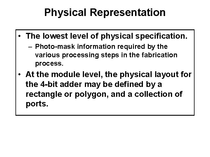
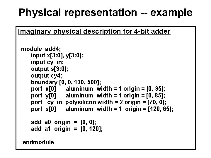
Physical Representation • The lowest level of physical specification. – Photo-mask information required by the various processing steps in the fabrication process. • At the module level, the physical layout for the 4 -bit adder may be defined by a rectangle or polygon, and a collection of ports.

Physical representation -- example Imaginary physical description for 4 -bit adder module add 4; input x[3: 0], y[3: 0]; input cy_in; output s[3: 0]; output cy 4; boundary [0, 0, 130, 500]; port x[0] aluminum width = 1 origin = [0, 35]; port y[0] aluminum width = 1 origin = [0, 85]; port cy_in polysilicon width = 2 origin = [70, 0]; port s[0] aluminum width = 1 origin = [120, 65]; add a 0 origin = [0, 0]; add a 1 origin = [0, 120]; endmodule

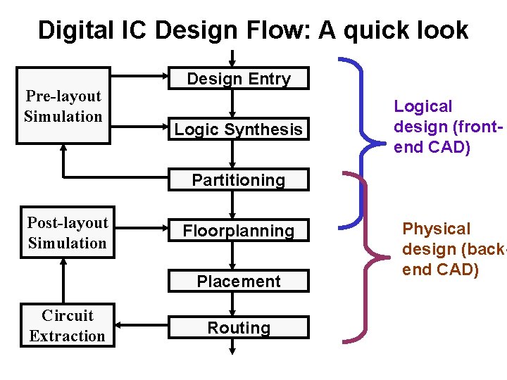
Digital IC Design Flow: A quick look Pre-layout Simulation Design Entry Logic Synthesis Logical design (frontend CAD) Partitioning Post-layout Simulation Floorplanning Placement Circuit Extraction Routing Physical design (backend CAD)