Electronic Circuits1CNET112 Level 4 th Department of CNET
![Common Collector[CC] Configuration In this configuration the input signal is applied between the base-collector Common Collector[CC] Configuration In this configuration the input signal is applied between the base-collector](https://slidetodoc.com/presentation_image_h/320fef270b30f3fb3b9049ae4f7735b6/image-14.jpg)


- Slides: 24

Electronic Circuits-1(CNET-112) Level 4 th Department of CNET College of CS & IS Jazan University KSA chapter-5

CHAPTER -5 TRANSISTORS Objectives In this Chapter, student will learn the following topics: Ø Introduction of Bipolar Junction Transistor(BJT) Ø Construction and Working of BJT Ø BJT Configuration Ø Regions of operation, Active, Cutoff, Saturation. Ø Amplifier Ø Voltage, Current and Power Amplifiers chapter-5

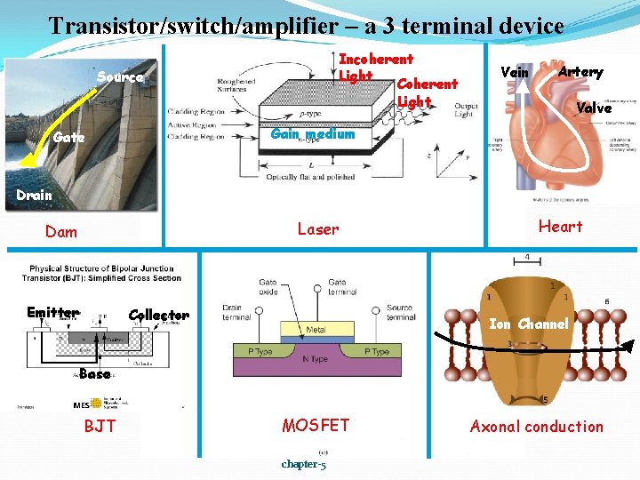
Transistor/switch/amplifier – a 3 terminal device Incoherent Light Coherent Light Source Vein Artery Valve Gain medium Gate Drain Laser Dam Emitter Collector Heart Ion Channel Base BJT MOSFET chapter-5 Axonal conduction

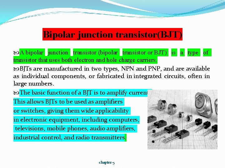
Bipolar junction transistor(BJT) A bipolar junction transistor (bipolar transistor or BJT) is a type of transistor that uses both electron and hole charge carriers. BJTs are manufactured in two types, NPN and PNP, and are available as individual components, or fabricated in integrated circuits, often in large numbers. The basic function of a BJT is to amplify current. This allows BJTs to be used as amplifiers or switches, giving them wide applicability in electronic equipment, including computers, televisions, mobile phones, audio amplifiers, industrial control, and radio transmitters. chapter-5

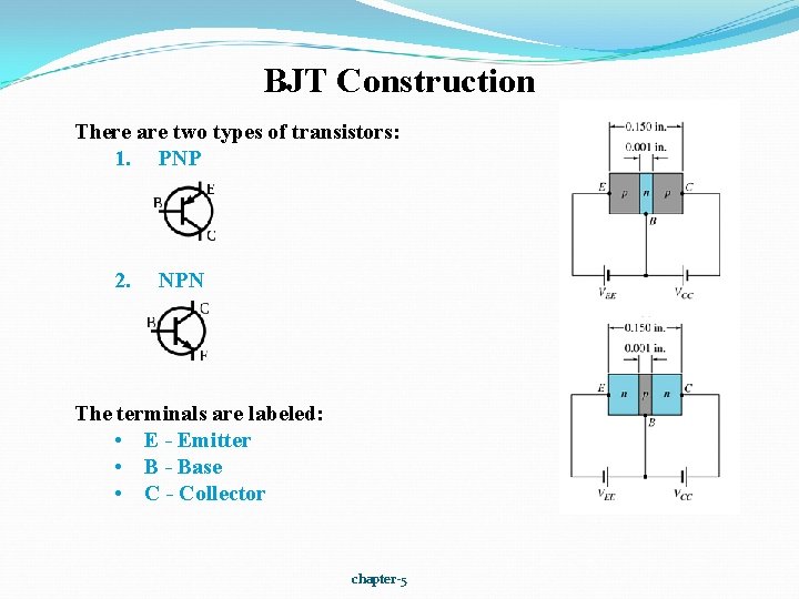
BJT Construction There are two types of transistors: 1. PNP 2. NPN The terminals are labeled: • E - Emitter • B - Base • C - Collector chapter-5

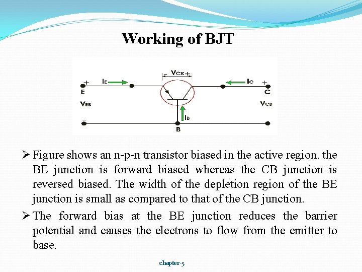
Working of BJT Ø Figure shows an n-p-n transistor biased in the active region. the BE junction is forward biased whereas the CB junction is reversed biased. The width of the depletion region of the BE junction is small as compared to that of the CB junction. Ø The forward bias at the BE junction reduces the barrier potential and causes the electrons to flow from the emitter to base. chapter-5

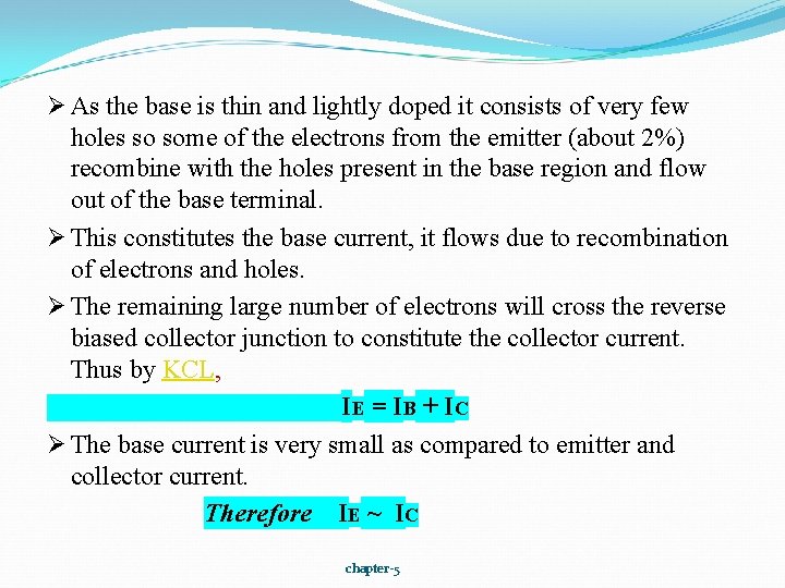
Ø As the base is thin and lightly doped it consists of very few holes so some of the electrons from the emitter (about 2%) recombine with the holes present in the base region and flow out of the base terminal. Ø This constitutes the base current, it flows due to recombination of electrons and holes. Ø The remaining large number of electrons will cross the reverse biased collector junction to constitute the collector current. Thus by KCL, IE = I B + I C Ø The base current is very small as compared to emitter and collector current. Therefore IE ~ IC chapter-5

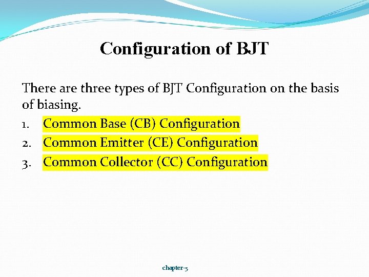
Configuration of BJT There are three types of BJT Configuration on the basis of biasing. 1. Common Base (CB) Configuration 2. Common Emitter (CE) Configuration 3. Common Collector (CC) Configuration chapter-5

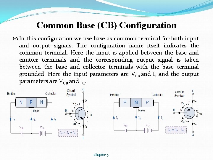
Common Base (CB) Configuration In this configuration we use base as common terminal for both input and output signals. The configuration name itself indicates the common terminal. Here the input is applied between the base and emitter terminals and the corresponding output signal is taken between the base and collector terminals with the base terminal grounded. Here the input parameters are VEB and IE and the output parameters are VCB and IC. chapter-5

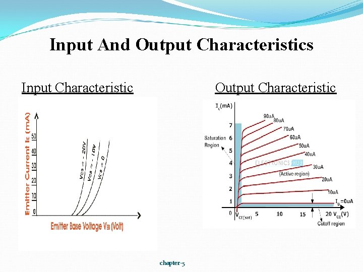
Input And Output Characteristics Input Characteristic Output Characteristic chapter-5

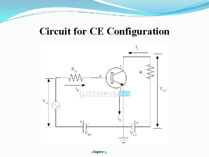
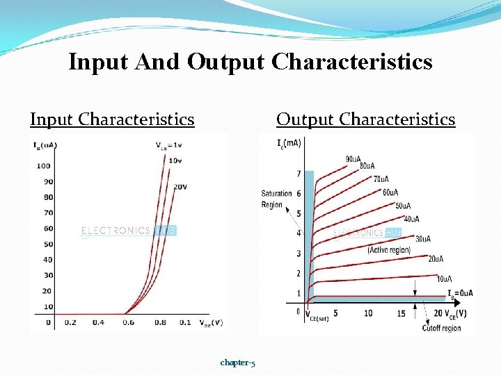
Common Emitter(CE) Configuration In this configuration we use emitter as common terminal for both input and output. Here the input is applied between base-emitter region and the output is taken between collector and emitter terminals. In this configuration the input parameters are VBE and IB and the output parameters are VCE and IC. chapter-5

Circuit for CE Configuration chapter-5

Input And Output Characteristics Input Characteristics Output Characteristics chapter-5
![Common CollectorCC Configuration In this configuration the input signal is applied between the basecollector Common Collector[CC] Configuration In this configuration the input signal is applied between the base-collector](https://slidetodoc.com/presentation_image_h/320fef270b30f3fb3b9049ae4f7735b6/image-14.jpg)
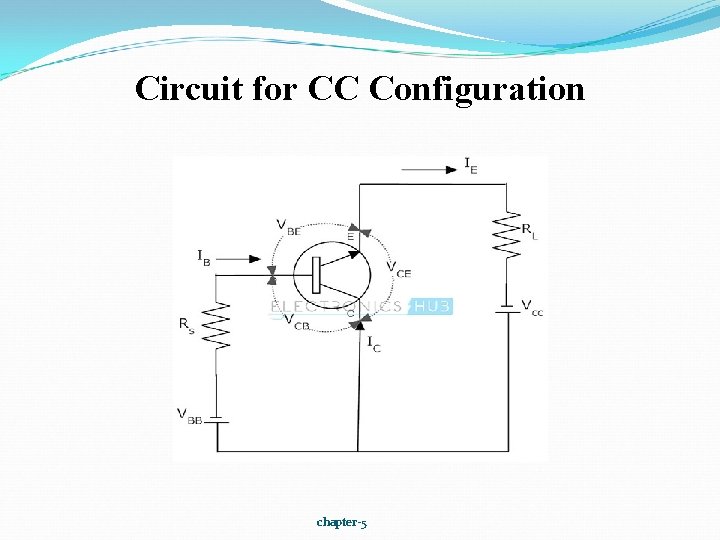
Common Collector[CC] Configuration In this configuration the input signal is applied between the base-collector region and the output is taken from the emitter-collector region. Here the input parameters are VBC and IB and the output parameters are VEC and IE. The common collector configuration has high input impedance and low output impedance. chapter-5

Circuit for CC Configuration chapter-5

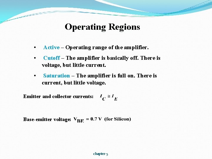
Operating Regions • Active – Operating range of the amplifier. • Cutoff – The amplifier is basically off. There is voltage, but little current. • Saturation – The amplifier is full on. There is current, but little voltage. Emitter and collector currents: Base-emitter voltage: chapter-5

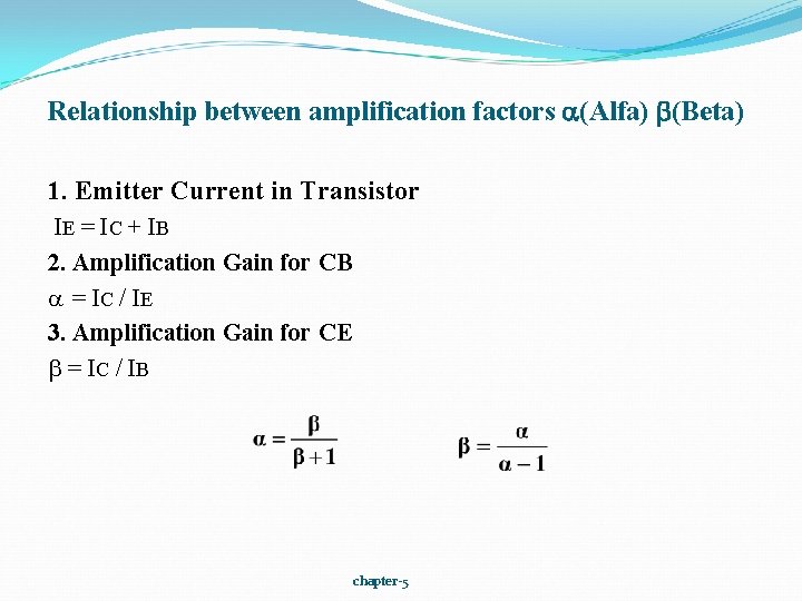
Relationship between amplification factors (Alfa) (Beta) 1. Emitter Current in Transistor IE = IC + IB 2. Amplification Gain for CB a = IC / IE 3. Amplification Gain for CE = IC / IB chapter-5

Transistor Characteristics chapter-5

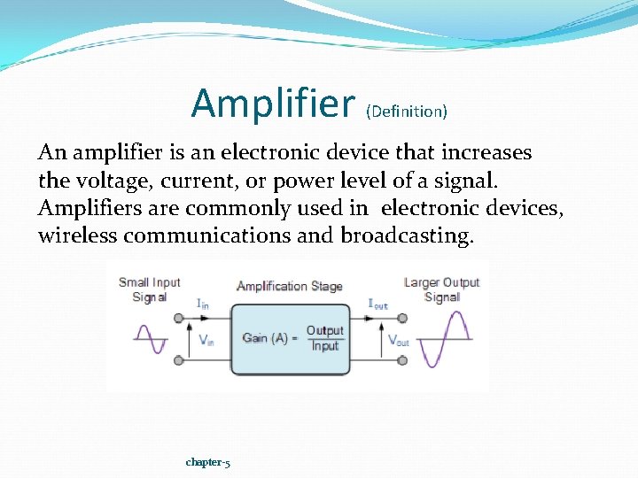
Amplifier (Definition) An amplifier is an electronic device that increases the voltage, current, or power level of a signal. Amplifiers are commonly used in electronic devices, wireless communications and broadcasting. chapter-5

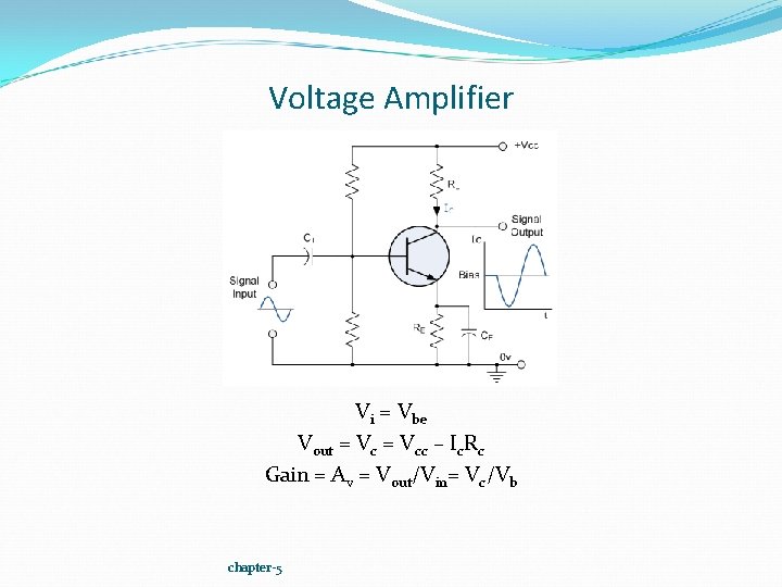
Voltage Amplifier Vi = Vbe Vout = Vcc – Ic. Rc Gain = Av = Vout/Vin= Vc/Vb chapter-5

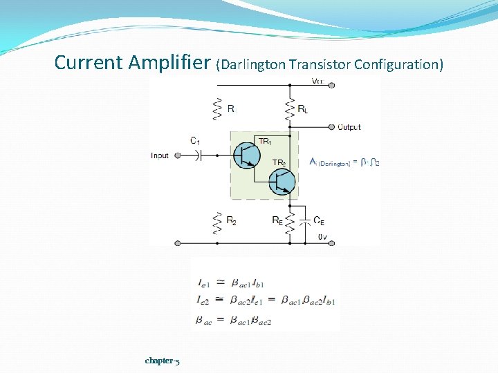
Current Amplifier (Darlington Transistor Configuration) chapter-5

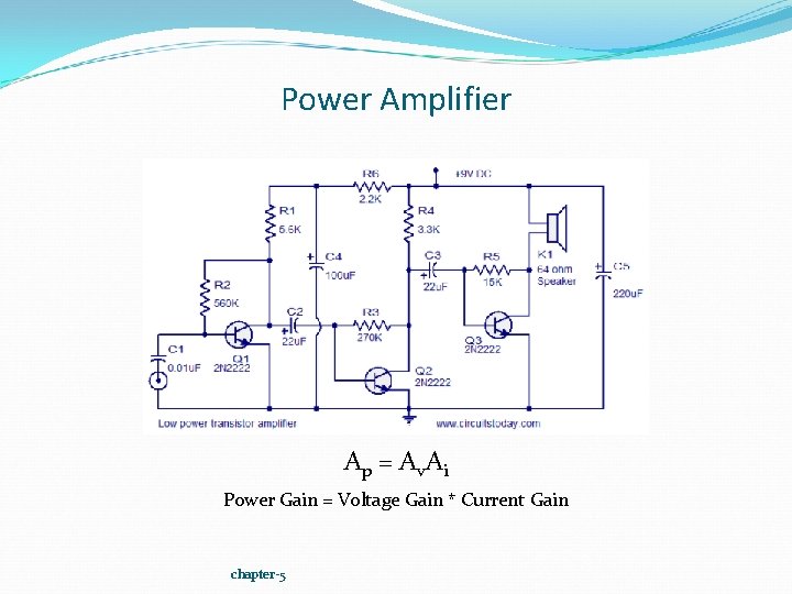
Power Amplifier Ap = Av. Ai Power Gain = Voltage Gain * Current Gain chapter-5

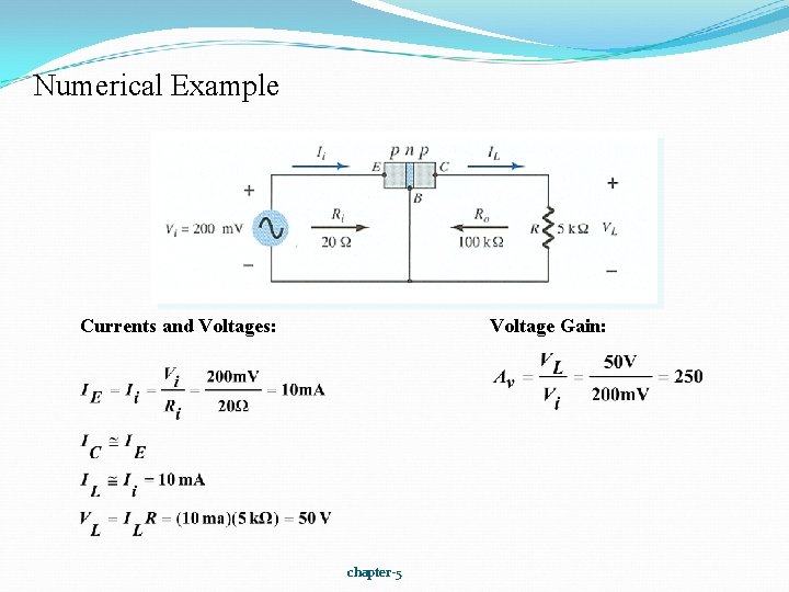
Numerical Example Currents and Voltages: Voltage Gain: chapter-5

Query chapter-5