Electronic Circuits 1 Atom The smallest part of


- Slides: 18
Electronic Circuits 1. Atom The smallest part of an element that preserves its characteristics is called “atom”. The number of positive charges (protons) in nucleus is equal to negative charges (electrons). In terms of electricity, an atom is charge less (neutral). At each shell, a known number of electrons can exist. The mathematical formula fort his number is shown below. Maximum Electron number = (Shell number)2 x 2 As an example, 3. shell can have at most 32 x 2=9 x 2=18 electrons. Except the outmost shell(called as valance shell), all shells must have their maximum number of electrons on them. The electrons that spin on the valance shell are called free electrons or valance electrons.
• 2. Conductor • • A good conducting atom has small number of valance electrons. As a general rule, a material is called conductor if it has less than 4 valance electrons, whereas the conductivity increases with decrease in the valance electrons. The best conductors are Silver, Gold and Copper atom has 1 valance electron, whereas Aluminum has 3 electrons, therefore we can conclude copper is a better conductor. When these valance electrons travel from an atom to another one, an electron flow emerges. That means an emerging electrical current.
• • 3. Insulator As a general rule, a material is called insulator if it has more than 4 valance electrons. A good insulator has more than 6 valance electrons. They do not give electrons, however they may absorb electrons in order to have 8 valance electrons. • 4. Semiconductor • • A material is called semiconductor if its atoms has exactly 4 valance electrons. In production of crystal diyotes and transistors, mostly Germanium and Silicon material is used. Semiconductors like Indium and Arsenic, are used as additional ingredients in production of those materials.
• 5. COVALENT BON • • The valance electrons of Silicon atom spins as if they are connected to the valance electrons of the neighboring atom. Each silicon atom has four valance pairs; these produce four difference electron bond pair. In order to pass electrical current from Silicon or Germanium, these valancebonds have to be torn apart by heat or voltage, which is indeed hard.
• • 6. N - TYPE SEMICONDUCTOR In order to form an easy electron movement, free electrons between the covalent bonds have to be revealed. To achieve this purpose, arsenic material is doped (added) to the main semiconductor (silicon or germanium) atoms. The main semiconductors have four valance electrons, whereas Arsenic has five valance electrons. When main semiconductor atom forms a covalent bond with arsenic atom, a valance electron of arsenic remains unbonded and moves freely. • The main carriers in N type material are electrons. In Figure, the distribution of carriers and ions in N type material is illustrated.
• • • 7. A P- TYPE SEMICONDUCTOR Forming a P type semiconductor has a similar methodology of forming an N type semiconductor, with the difference that Indium atoms are doped into main semiconductor atoms. Indium atom has 3 valance electrons; therefore the mixed atoms have an electron deficiency in formed covalent bond. These deficiencies are called holes. This formation is depicted in Figure. The main carriers in P type material are electrons. In Figure , the distribution of carriers and ions in P type material is illustrated.
• 8. FORMATION OF A P-N JUNCTION DIODE • In Figure 8. 9, the distribution of ions and carriers in P and N type materials are illustrated. If these two types are connected, positive and negative ions gathers in the junction area. • • • The P and N type materials form Anode and Cathode of the diode, respectively. The circuit symbol of the diode is shown in Figure
• • • REVERSE BIAS TO P-N JUNCTION Negative and positive potentials are applied to P and N type materials, respectively, as shown in Figure 8. 12. The electrons of N type material is pulled by the “+” pole of the source. Similarly, the holes of N type material near the junction surface is filled by the “- “ pole of the source. In this situation, the result is the enlargement of the depletion layer. The diffusion of majority carrier is getting harder. Meanwhile, a small amount of minority current carriers produce a small circuit current. This is called “reverse saturation current”, which generally in the order of micro amperes
FORWARD BIAS TO P-N JUNCTION Positive and negative potentials are applied to P and N type materials, respectively, as shown in Figure. Majority carrier current remains same. By following same arguments in reverse bias, the depletion layer diminishes; therefore high amount of flow of majority carriers is observed The flow of majority carriers increases with the increase in the applied voltage. I. and III regions show positive and negative bias regions, respectively.
• • • If we examine the forward bias region in Figure , the current passing increases at a noticeable rate when the applied voltage is 0. 1 Volts and 0. 7 Volts. These voltage values are called “built in potential” or on voltage. Summarizing above, built in potential is the smallest voltage value Ek voltage value is sufficient value that usually damages the diode. If the voltage is beyond Ek value, the diode will be damaged and a big current in the reverse direction will flow, which is called avalanche current, which renders the diode useless. hat allows a diode to conduct. The Ek voltage that is shown in the reverse bias region is called breakdown voltage.
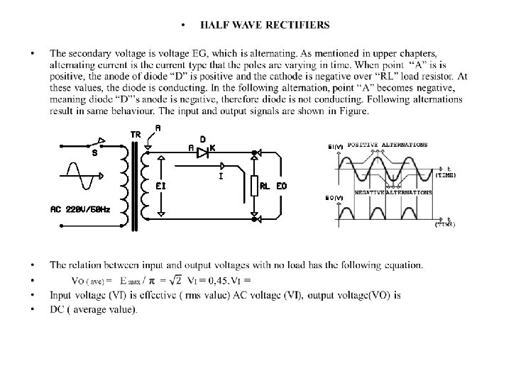
9. DIOD AS RECTIFIER • • • Nearly all of today’s widely used electronic devices (radio, tv, personal computers, etc) works with direct current (DC). Most economic way to obtain direct current is using city electric network. However, the distributed electricity is alternating current (AC). The circuits or devices that convert alternating current to direct current are called rectifiers. Rectifiers mainly fall into two groups: 1 - Half wave rectifiers 2 - Full wave rectifiers • • • Peak to peak voltage (Epp) and current (Ipp); Epp = 2. Emax Ipp = 2. Imax Effective voltage (E) & current (I); E = 0, 707. Emax I = 0, 707. Imax Instantaneous voltage (e) ve current (i); e = Emax. sinθ. i = Imax. • • • The change in the alternating current in the period is called “sinusoidal change” or “sinusoidal curve”. The horizontal axis is time axis. For defining a point on the time axis, generally angle with unit of degree is used. The upper and lower parts of time axis are positive (+) and negative(-) areas, respectively.
• • • Example: Electricity network has an effective voltage of 220 V. Evaluate maximum and peak to peak voltages. Solution: E = 0, 707. Emax Volt • • Epp = 2. Emax Epp = 2. 311, 1=
• • Typical working voltages of electronic devices are generally much lower then the city network. For operating these devices, the ciy electricity voltage must be lowered. This operation is accomplished by using transformers. Transformers are circuit components working in alternating current.
FULL WAVE RECTIFIER • A good direct voltage can not be obtained by half wave rectifiers since they conduct only in one alternation. This problem is solved in full wave rectifiers in which the input signal is used in both alternations. In order to produce a full wave rectifier, a transformer with middle pinned secondary is needed to be used. For a moment, if we seperae the middle pin of a middle pinned secondary, the sign of the output pins with respect to the sign of the input are shown in Figure. • Positive half cycle Negitive half cycle
• The cathodes of diodes D 1 and D 2 are always connected to zero voltage over a load resistor. The signs of A and D points change with respect to the frequency of the signal. Assume point A is positive and point D is negative. At this moment, D 1 is conducting and D 2 is not conducting because of the anode voltages. In the second alternation, point A becomes negative and point D becomes positive. D 1 is not conducting and D 2 is conducting because of the signals in their anodes. Observe that only one diode is conducting at each alternation. • • The relation between input and output voltages with no load has the following mathematical representation. Vo=0, 9. Vi Input voltage (Vi) is effective AC voltage (Vi) , output voltage(Vo) is DC.
BRIDGE FULL WAVE RECTIFIER • • • A bridge full wave rectifier is shown in Figure 9. 21. These type of rectifiers does not use middle pinned transormers. The peak to peak voltage is applied to the pins of two diodes that are serially connected. At most half of the applied voltage can be seen at each diodes pin. The current directions for two sequential anternations are showed in Figure 9. 22 and Figure 9. 23. Figure 9. 21 Figure 9. 22
• The sign over the load is same as standart full wave rectifiers, with the only difference 0. 7 volt amplitude difference. The relation between input and output voltages with no load has the following mathematical representation. • • Vo = (0, 9. VI ) − 0, 7 Input voltage (Vi) is effective AC voltage (Vi), output voltage (Vo) is DC.