ELECTRON MICROSCOPY University of Mumbai Department of Chemistry
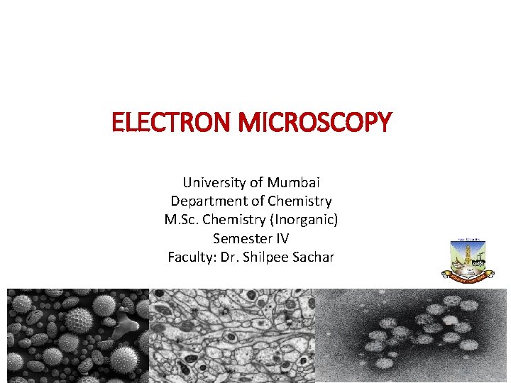
ELECTRON MICROSCOPY University of Mumbai Department of Chemistry M. Sc. Chemistry (Inorganic) Semester IV Faculty: Dr. Shilpee Sachar
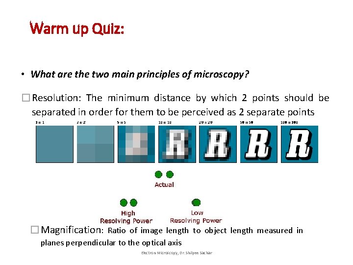
Warm up Quiz: • What are the two main principles of microscopy? �Resolution: The minimum distance by which 2 points should be separated in order for them to be perceived as 2 separate points �Magnification: Ratio of image length to object length measured in planes perpendicular to the optical axis Electron Microscopy, Dr. Shilpee Sachar
Warm up Quiz: • What are the most common types of microscopes? �Optical Microscope, that uses light to image the sample �Electron Microscope, that uses electron beam for imaging �Scanning Probe Microscope, that uses a physical probe to scan the objects Electron Microscopy, Dr. Shilpee Sachar
Warm up Quiz: • What is the typical magnification and resolution of an optical microscope? �Typical Magnification: 1500 x �Resolution: 200 nm Specialized techniques may exceed the magnification but the resolution is limited by the wavelength of the imaging radiation used Electron Microscopy, Dr. Shilpee Sachar
Warm up Quiz: • What are the typical resolution and magnification of an Electron Microscope? • Typical resolving power of Electron Microscope is 50 pm (0. 05 nm) • Magnification possible with an Electron Microscope is 10, 000 x Electron Microscopy, Dr. Shilpee Sachar
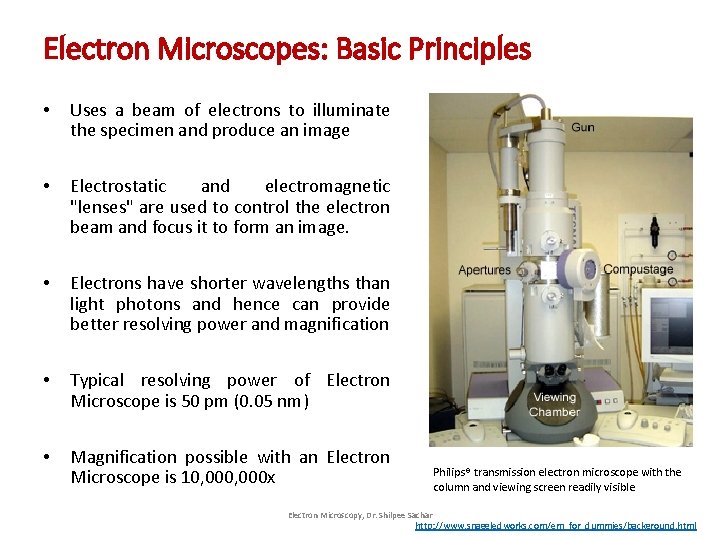
Electron Microscopes: Basic Principles • Uses a beam of electrons to illuminate the specimen and produce an image • Electrostatic and electromagnetic "lenses" are used to control the electron beam and focus it to form an image. • Electrons have shorter wavelengths than light photons and hence can provide better resolving power and magnification • Typical resolving power of Electron Microscope is 50 pm (0. 05 nm) • Magnification possible with an Electron Microscope is 10, 000 x Philips® transmission electron microscope with the column and viewing screen readily visible Electron Microscopy, Dr. Shilpee Sachar http: //www. snaggledworks. com/em_for_dummies/background. html
How can Electron Microscopes be used? Electron Microscopes can yield the following information: • Topography : The surface features of an object or "how it looks", its texture; direct relation between these features and materials properties (hardness, reflectivity. . . etc. ) • Morphology : The shape and size of the particles making up the object; direct relation between these structures and materials properties (ductility, strength, reactivity. . . etc. ) • Composition: The elements and compounds that the object is composed of and the relative amounts of them; direct relationship between composition and materials properties (melting point, reactivity, hardness. . . etc. ) • Crystallographic Information : How the atoms are arranged in the object; direct relation between these arrangements and materials properties (conductivity, electrical properties, strength. . . etc. ) Electron Microscopy, Dr. Shilpee Sachar
History of Electron Microscopes • Similarity of cathode rays with light rays was established by Hertz and Weichart in late 19 th century • The first prototype of electron microscope was built by German engineer Ernst Ruska in 1933. It had a resolution power of 50 nm • Ruska was recognized for his invention 50 years later by award of a Nobel Prize • The first commercially available electron microscope was built in England by Metropolitan Vickers for Imperial College, London; but the product did not take off very well due to several limitations • At the University of Toronto, in 1938, Eli Franklin Burton and students Cecil Hall, James Hillier and Albert Prebus constructed the first electron microscope in the New World; the design eventually led to RCA (Radio Corporation of America) range of very successful microscopes. Electron Microscopy, Dr. Shilpee Sachar https: //www. newworldencyclopedia. org/entry/Electron_microscope
Working Principle of Electron Microscopes • Electron Microscopes(EMs) use a focused beam of electrons to "image" the specimen and gain information as to its structure and composition. • The basic steps involved in all EMs: • A stream of electrons is formed (by the Electron Source) and accelerated toward the specimen using a positive electrical potential • This stream is confined and focused using metal apertures and magnetic lenses into a thin, focused, monochromatic beam. • This beam is focused onto the sample using a magnetic lens • Interactions occur inside the irradiated sample, affecting the electron beam • These interactions and effects are detected and transformed into an image • The above steps are carried out in all EMs regardless of type Electron Microscopy, Dr. Shilpee Sachar
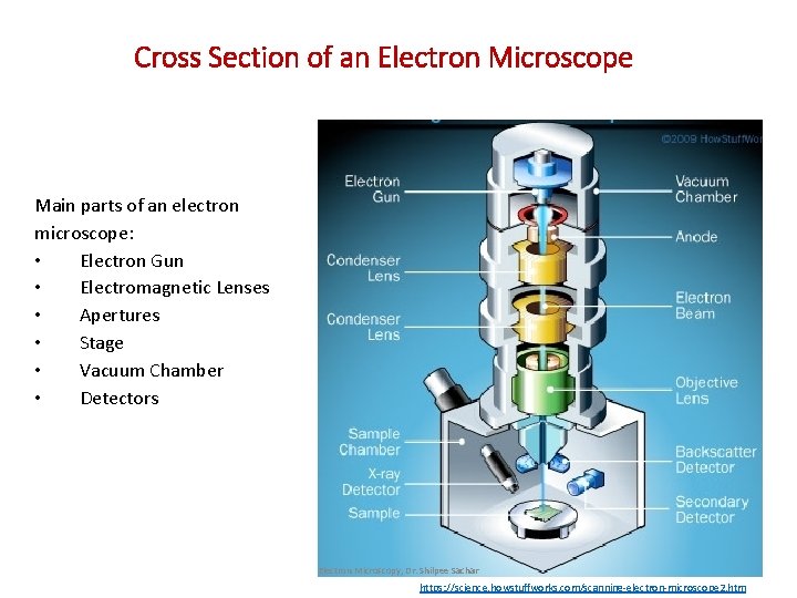
Cross Section of an Electron Microscope Main parts of an electron microscope: • Electron Gun • Electromagnetic Lenses • Apertures • Stage • Vacuum Chamber • Detectors Electron Microscopy, Dr. Shilpee Sachar https: //science. howstuffworks. com/scanning-electron-microscope 2. htm
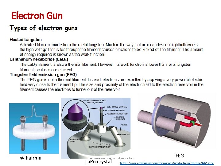
Electron Gun W hairpin Electron Microscopy, Dr. Shilpee Sachar La. B 6 crystal FEG https: //www. emsdiasum. com/microscopy/products/microscope/lab 6. aspx
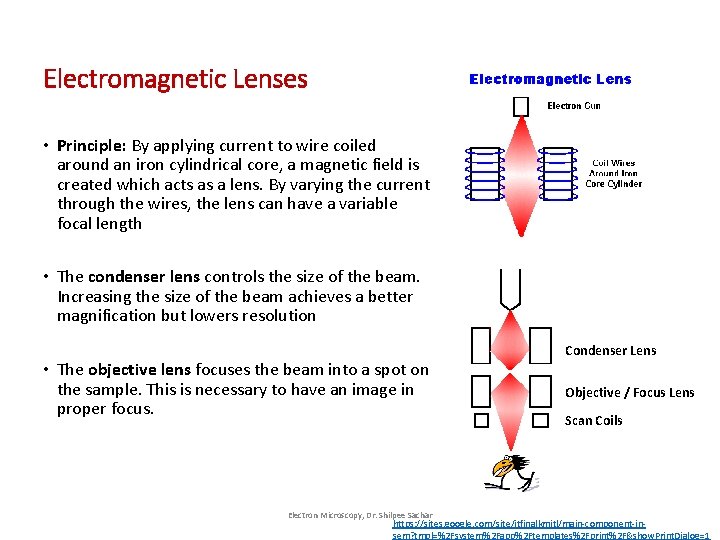
Electromagnetic Lenses • Principle: By applying current to wire coiled around an iron cylindrical core, a magnetic field is created which acts as a lens. By varying the current through the wires, the lens can have a variable focal length • The condenser lens controls the size of the beam. Increasing the size of the beam achieves a better magnification but lowers resolution • The objective lens focuses the beam into a spot on the sample. This is necessary to have an image in proper focus. Electron Microscopy, Dr. Shilpee Sachar Condenser Lens Objective / Focus Lens Scan Coils https: //sites. google. com/site/itfinalkmitl/main-component-insem? tmpl=%2 Fsystem%2 Fapp%2 Ftemplates%2 Fprint%2 F&show. Print. Dialog=1
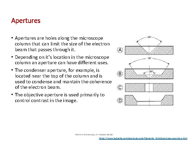
Apertures • Apertures are holes along the microscope column that can limit the size of the electron beam that passes through it. • Depending on it's location in the microscope column an aperture can have different uses. • The condenser aperture, for example, is located near the top of the column and is used to condense and mantain the coherence of the electron beam. • The objective aperture is used primarily to control contrast in the image. Electron Microscopy, Dr. Shilpee Sachar https: //www. tedpella. com/apertures-and-filaments_html/apertures-overview. htm
Types of Electron Microscope • Transmission Electron Microscope (TEM) • Electron Beam is passed through a very thin specimen. • The transmitted electron carry information about the structure and composition of the specimen • The spatial variation in the electrons is then magnified using magnetic lenses to produce an image on a fluorescent screen • Scanning Electron Microscope (SEM) • Electron beam is used to scan the specimen • The electron beam interacts with the specimen and secondary electrons are emitted from the surface of the specimen • Detectors are used to identify the pattern of the secondary electrons which in turn is used to form the image Electron Microscopy, Dr. Shilpee Sachar
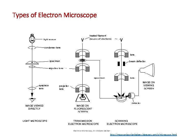
Types of Electron Microscope Electron Microscopy, Dr. Shilpee Sachar http: //msseconisseniorbiology. blogspot. com/p/microscopy. html
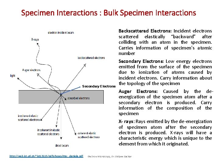
Specimen Interactions : Bulk Specimen Interactions • Backscattered Electrons: Incident electrons scattered elastically “backward” after colliding with an atom in the specimen. Carries information of specimen’s atomic number • Secondary Electrons: Low energy electrons emitted from the surface of the specimen due to ionization of atoms caused by incident electrons. Carry information about the topology of the specimen Secondary Electrons http: //web. ist. utl. pt/~ist 13115/pdfs/teses/msc_daniela. pdf • Auger Electrons: Caused by the deenergization of the specimen atom after a secondary electron is produced. Carry information of the composition of the specimen • X- rays: Rays emitted by the de-energization of specimen atom after the secondary electron is produced. X-rays will have a characteristic energy which is unique to the element from which it originated. Electron Microscopy, Dr. Shilpee Sachar
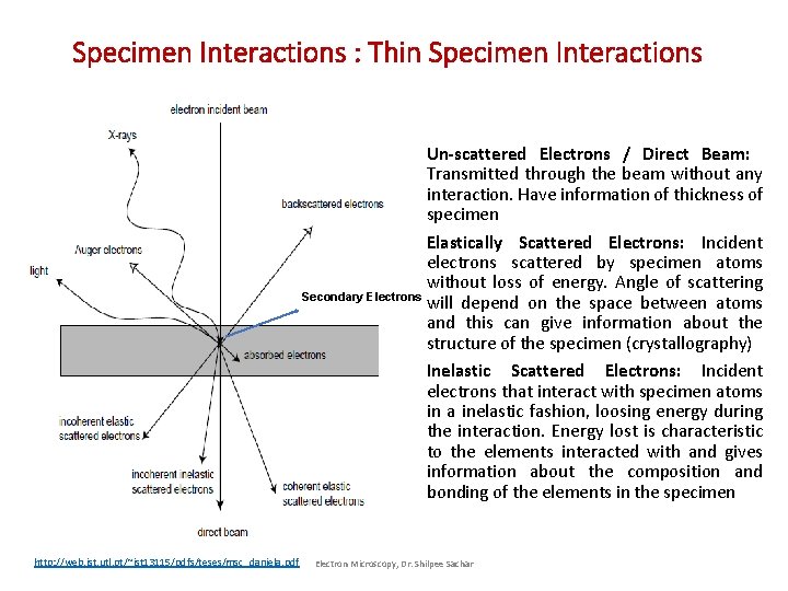
Specimen Interactions : Thin Specimen Interactions • Un-scattered Electrons / Direct Beam: Transmitted through the beam without any interaction. Have information of thickness of specimen Elastically Scattered Electrons: Incident electrons scattered by specimen atoms without loss of energy. Angle of scattering Secondary Electrons will depend on the space between atoms and this can give information about the structure of the specimen (crystallography) • • http: //web. ist. utl. pt/~ist 13115/pdfs/teses/msc_daniela. pdf Inelastic Scattered Electrons: Incident electrons that interact with specimen atoms in a inelastic fashion, loosing energy during the interaction. Energy lost is characteristic to the elements interacted with and gives information about the composition and bonding of the elements in the specimen Electron Microscopy, Dr. Shilpee Sachar
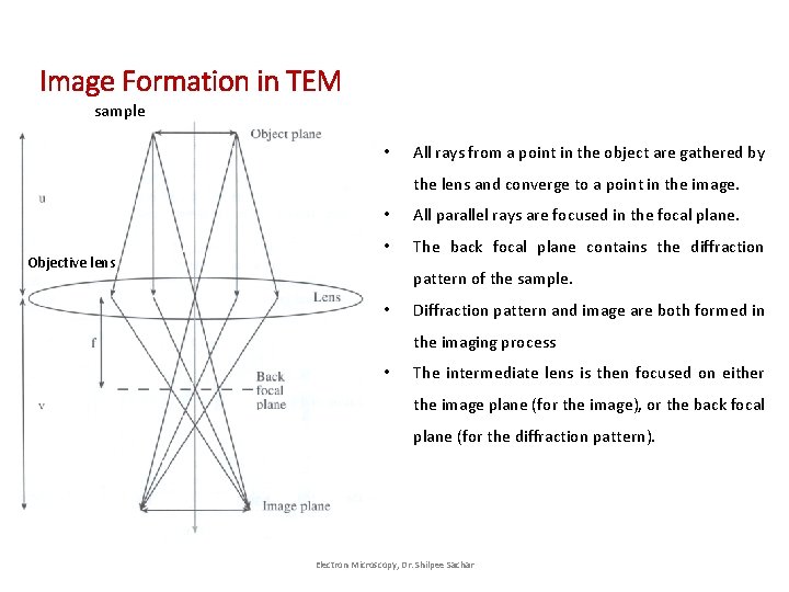
Image Formation in TEM sample • All rays from a point in the object are gathered by the lens and converge to a point in the image. Objective lens • All parallel rays are focused in the focal plane. • The back focal plane contains the diffraction pattern of the sample. • Diffraction pattern and image are both formed in the imaging process • The intermediate lens is then focused on either the image plane (for the image), or the back focal plane (for the diffraction pattern). Electron Microscopy, Dr. Shilpee Sachar
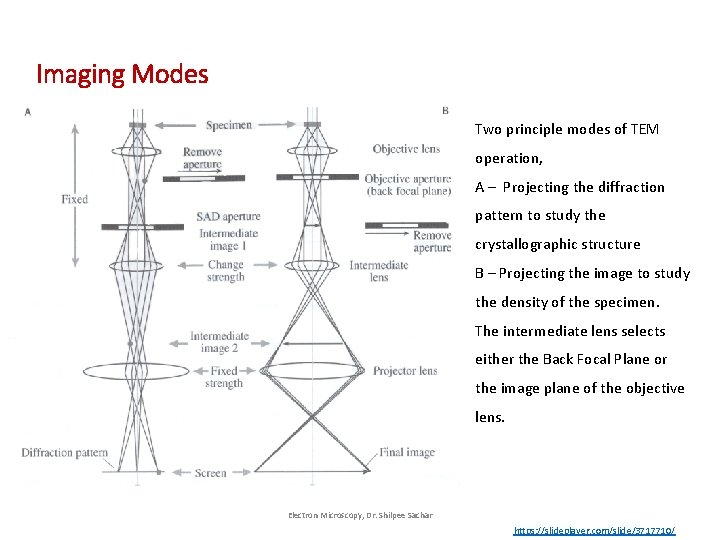
Imaging Modes Two principle modes of TEM operation, A – Projecting the diffraction pattern to study the crystallographic structure B – Projecting the image to study the density of the specimen. The intermediate lens selects either the Back Focal Plane or the image plane of the objective lens. Electron Microscopy, Dr. Shilpee Sachar https: //slideplayer. com/slide/3717710/
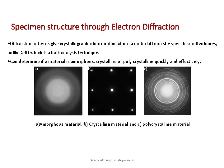
Specimen structure through Electron Diffraction • Diffraction patterns give crystallographic information about a material from site specific small volumes, unlike XRD which is a bulk analysis technique. • Can determine if a material is amorphous, crystalline or poly crystalline quickly and effectively. a) b) c) a)Amorphous material, b) Crystalline material and c) polycrystalline material Electron Microscopy, Dr. Shilpee Sachar
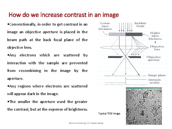
How do we increase contrast in an image • Conventionally, in order to get contrast in an image an objective aperture is placed in the beam path at the back focal plane of the objective lens. • Any electrons which are scattered by interaction with the sample are prevented from recombining in the image by the aperture. • Any regions where electrons are scattered will appear dark in the image. • The smaller the aperture used the greater the contrast, but at the expense of brightness. Typical TEM image Electron Microscopy, Dr. Shilpee Sachar
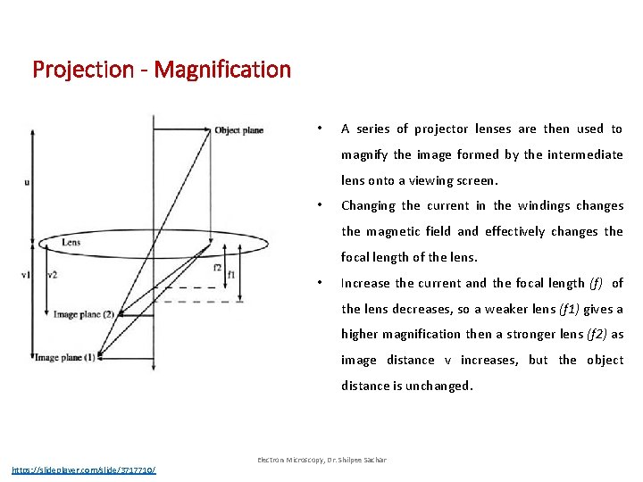
Projection - Magnification • A series of projector lenses are then used to magnify the image formed by the intermediate lens onto a viewing screen. • Changing the current in the windings changes the magnetic field and effectively changes the focal length of the lens. • Increase the current and the focal length (f) of the lens decreases, so a weaker lens (f 1) gives a higher magnification then a stronger lens (f 2) as image distance v increases, but the object distance is unchanged. https: //slideplayer. com/slide/3717710/ Electron Microscopy, Dr. Shilpee Sachar
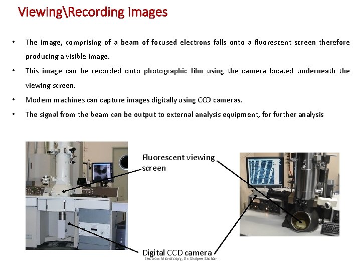
ViewingRecording Images • The image, comprising of a beam of focused electrons falls onto a fluorescent screen therefore producing a visible image. • This image can be recorded onto photographic film using the camera located underneath the viewing screen. • Modern machines can capture images digitally using CCD cameras. • The signal from the beam can be output to external analysis equipment, for further analysis Fluorescent viewing screen Digital CCD camera Electron Microscopy, Dr. Shilpee Sachar
Sample Preparation for TEM • Samples are typically 3 mm in diameter and <80µm thick. • Sample preparation is tricky and time consuming. • Very thin slices of specimen can be cut from a piece of tissue either by fixing it in plastic or working with it as frozen material • Specimen can be stained in different ways and markers can be used to locate specific things in the tissue. Electron Microscopy, Dr. Shilpee Sachar
Sample Preparation for Metallic Samples • Cutslice a section of material <1 mm thick. • Produce 3 mm diameter blanks by either Punching, or spark erosion. • Grind and polish blanks to <80µm thick and 0. 25µm or better finish. • For Al based alloys, due to build up of Al 2 O 3 coatings in the presence of air, the samples should be examined immediately after preparation. Electron Microscopy, Dr. Shilpee Sachar
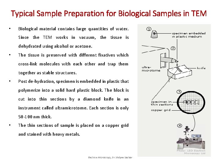
Typical Sample Preparation for Biological Samples in TEM • Biological material contains large quantities of water. Since the TEM works in vacuum, the tissue is dehydrated using alcohol or acetone. • The tissue is preserved with different fixatives which cross-link molecules with each other and trap them together as stable structures. • Post de-hydration, specimen is embedded in plastic that polymerize into a solid hard plastic block. The block is cut into thin sections by a diamond knife in an instrument called ultramicrotome. Each section is only 50 -100 nm thick. • The thin sections of sample is placed on a copper grid and stained with heavy metals. Electron Microscopy, Dr. Shilpee Sachar
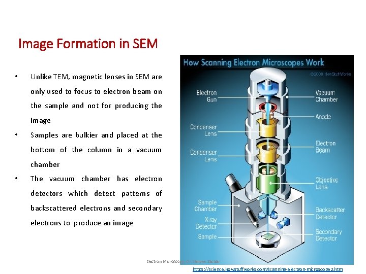
Image Formation in SEM • Unlike TEM, magnetic lenses in SEM are only used to focus to electron beam on the sample and not for producing the image • Samples are bulkier and placed at the bottom of the column in a vacuum chamber • The vacuum chamber has electron detectors which detect patterns of backscattered electrons and secondary electrons to produce an image Electron Microscopy, Dr. Shilpee Sachar https: //science. howstuffworks. com/scanning-electron-microscope 2. htm
Detection of Secondary Electrons in SEM • Low-energy secondary electrons close to the specimen surface are detected by an Everhart. Thornley detector system • The secondary electrons are first collected by attracting them towards an electrically biased grid (+400 V) and then further accelerated towards a scintillator positively biased to about +2, 000 V. • The accelerated secondary electrons cause the scintillator to emit flashes of light which are conducted to a photomultiplier outside the SEM column. • The amplified electrical signal output by the photomultiplier is displayed as a twodimensional intensity distribution that can be viewed and photographed • Secondary electrons carry information of the topography of the specimen • Steep surfaces and edges tend to be brighter than flat surfaces, which results in images with a well-defined, three-dimensional appearance. Electron Microscopy, Dr. Shilpee Sachar
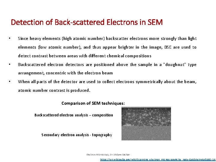
Detection of Back-scattered Electrons in SEM • Since heavy elements (high atomic number) backscatter electrons more strongly than light elements (low atomic number), and thus appear brighter in the image, BSE are used to detect contrast between areas with different chemical compositions • Backscattered electron detectors are positioned above the sample in a "doughnut" type arrangement, concentric with the electron beam • When all parts of the detector are used to collect electrons symmetrically about the beam, atomic number contrast is produced. Comparison of SEM techniques: Backscattered electron analysis – composition Secondary electron analysis - topography Electron Microscopy, Dr. Shilpee Sachar https: //en. wikipedia. org/wiki/Scanning_electron_microscope#cite_note-Goldsteinetal 1981 -14
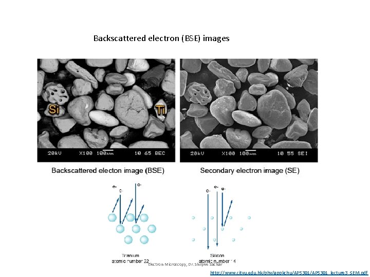
Backscattered electron (BSE) images Electron Microscopy, Dr. Shilpee Sachar http: //www. cityu. edu. hk/phy/appkchu/AP 5301_lecture 3_SEM. pdf
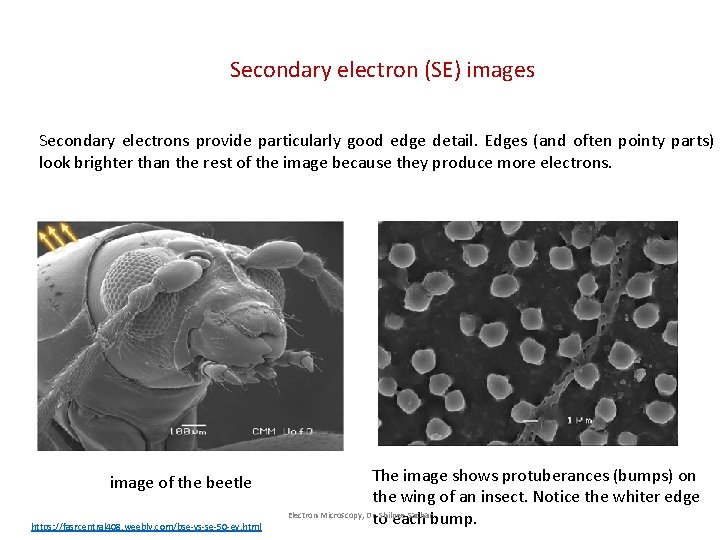
Secondary electron (SE) images Secondary electrons provide particularly good edge detail. Edges (and often pointy parts) look brighter than the rest of the image because they produce more electrons. image of the beetle https: //fasrcentral 408. weebly. com/bse-vs-se-50 -ev. html The image shows protuberances (bumps) on the wing of an insect. Notice the whiter edge Electron Microscopy, Dr. Shilpee Sachar to each bump.
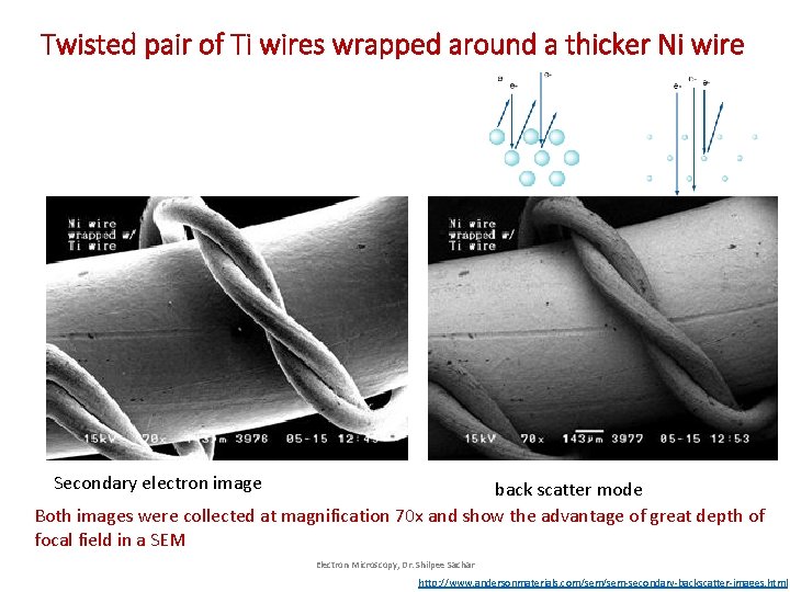
Twisted pair of Ti wires wrapped around a thicker Ni wire Secondary electron image back scatter mode Both images were collected at magnification 70 x and show the advantage of great depth of focal field in a SEM Electron Microscopy, Dr. Shilpee Sachar http: //www. andersonmaterials. com/sem-secondary-backscatter-images. html
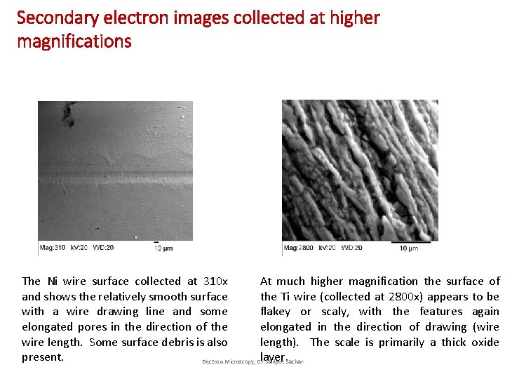
Secondary electron images collected at higher magnifications The Ni wire surface collected at 310 x At much higher magnification the surface of and shows the relatively smooth surface the Ti wire (collected at 2800 x) appears to be with a wire drawing line and some flakey or scaly, with the features again elongated pores in the direction of the elongated in the direction of drawing (wire length. Some surface debris is also length). The scale is primarily a thick oxide present. layer. Electron Microscopy, Dr. Shilpee Sachar
Comparison of TEM & SEM techniques • SEM focuses on the sample’s surface and its composition. On the other hand, TEM seeks to see what is inside or beyond the surface. • SEM also shows the sample bit by bit while TEM shows the sample as a whole. • In SEM sample is coated with a thin layer of a heavy metal such as gold or palladium while the sample in TEM has to be cut thinner (70 -90 nm) because electrons cannot penetrate very far into materials. . • SEM also provides a three-dimensional image while TEM delivers a twodimensional picture. • In terms of magnification and resolution, TEM has an advantage compared to SEM. TEM has up to a 50 million magnification level while SEM only offers 2 million as a maximum level of magnification. • The resolution of TEM is 0. 5 angstroms while SEM has 0. 4 nanometers. Electron Microscopy, Dr. Shilpee Sachar
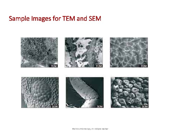
Sample Images for TEM and SEM Electron Microscopy, Dr. Shilpee Sachar
Electron Microscopy – An expensive affair • Expensive to buy and maintain • Dynamic in operation; require extremely stable high voltage supplies, extremely stable currents to each electromagnetic coil/lens, continuouslypumped high/ultra-high vacuum systems and a cooling water supply circulation through the lenses and pumps. • Very sensitive to vibration and external magnetic fields, hence must be housed in buildings with special services. • It’s a specialized skill; significant amount of training is required in order to operate an electron microscope successfully • Samples need to be specially prepared by sometimes lengthy and difficult techniques to withstand the environment inside an electron microscope Electron Microscopy, Dr. Shilpee Sachar
References • D. A. Skoog and F. J. Holler and T. A. Nieman, Principles of instrumental analysis, 5 th ed. , Harcourt Asia PTE Ltd. (1998). • R. A. Scott and C. M. Lukehart, Applications of physical methods to inorganic and bioinorganic chemistry, John Wiley & Sons Ltd. (2007). • Sulabha K. Kulkarni, Nanotechnology: Principles and practices, Capital publishing company (2007). • Goldstein, G. I. ; Newbury, D. E. ; Echlin, P. ; Joy, D. C. ; Fiori, C. ; Lifshin, E. (1981). Scanning electron microscopy and x-ray microanalysis. New York: Plenum Press. ISBN 978 -0 -306 -40768 -0. • Transmission Electron Microscopy of Biological Samples, Łukasz Mielańczyk, Natalia Matysiak, Olesya Klymenko and Romuald Wojnicz • Zhou W. , Apkarian R. , Wang Z. L. , Joy D. (2006) Fundamentals of Scanning Electron Microscopy (SEM). In: Zhou W. , Wang Z. L. (eds) Scanning Microscopy for Nanotechnology. Springer, New York, NY • Transmission Electron Microscopy of Shape-Controlled Nanocrystals and Their Assemblies, Z. L. Wang*, The Journal of Physical Chemistry B 2000 104 (6), 1153 -1175, DOI: 10. 1021/jp 993593 c. • Łukasz Mielańczyk, Natalia Matysiak, Olesya Klymenko and Romuald Wojnicz (September 2 nd 2015). Transmission Electron Microscopy of Biological Samples, The Transmission Electron Microscope - Theory and Applications, Khan Maaz, Intech. Open, DOI: 10. 5772/60680. Available from: https: //www. intechopen. com/books/the-transmissionelectron-microscope-theory-and-applications/transmission-electron-microscopy-of-biological-samples • https: //www. newworldencyclopedia. org/entry/Electron_microscope • https: //microbeonline. com/difference-electron-microscopy-between-sem-tem/ • http: //www. cityu. edu. hk/phy/appkchu/AP 5301_lecture 3_SEM. pdf • http: //www. andersonmaterials. com/sem-secondary-backscatter-images. html • http: //www. iaszoology. com/tem/ Electron Microscopy, Dr. Shilpee Sachar
- Slides: 37