Electron Energy Loss Spectroscopy EELS Atomicscale view of
 张 庶 元")


 imaging filter (GIF). Attached to the TEM column below")
 § Spectrum is enlarged and optimally coupled to")
 § The spectrum is shifted § Best to")

 § § The spectrum is shifted relative")


 –")


- Slides: 33
电子能量损失谱 Electron Energy Loss Spectroscopy (EELS) 张 庶 元
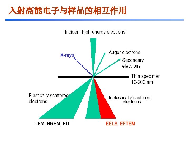
Atomic-scale view of electron energy loss in TEM Incident beam electron E 0 (100 to 1000 ke. V) Excited specimen electron EB + E Scattered beam electron E 0 - E 3
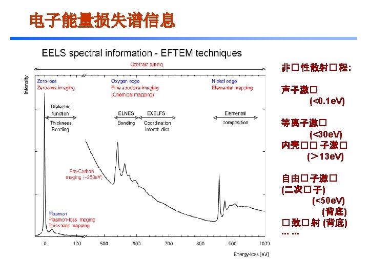
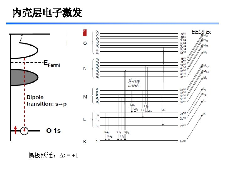
What is an EELS spectrum? Elastic scattering Inelastic scattering L L K Carbon K atom Electrons count Zero loss CK 1 e. V 0 290 Electron energy loss (e. V)
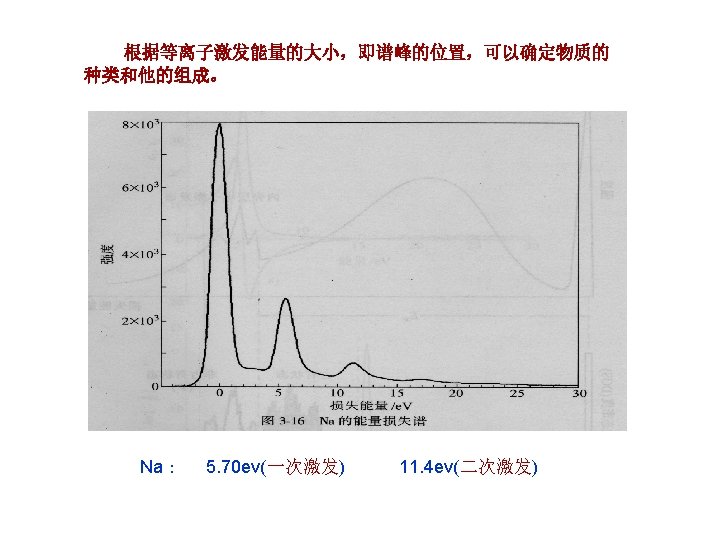
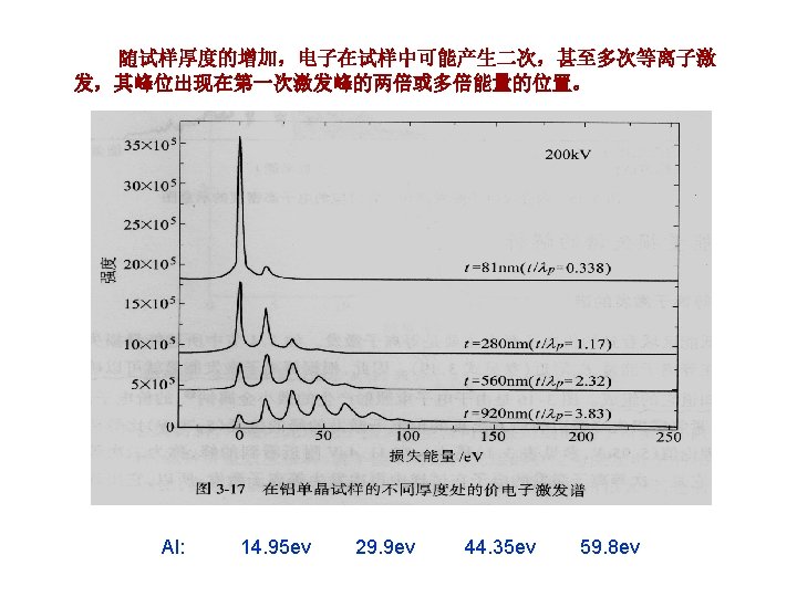
Specimen thickness measurement λ 为电子非弹性散射的平均自由程 IT 为第一个等离激发峰的强度 Io 为零损失峰的强度 Rough estimate of λ : λ ~ 0. 8 Eo nm so for 100 -ke. V electrons λ is 80 -120 nm various materials
Correlation between EELS and specimen feature 11
Magnetic prism spectrometer
EELS spectrometer Optical configuration at entrance Dispersion and focusing section Projection section Spectrum plane 13
In-column omega-filter Inserted in the imaging lens system Energy-filter imaging and electron diffraction, CBED
Post-column imaging filter Gatan (Tridiem) imaging filter (GIF). Attached to the TEM column below the viewing chamber
Energy-loss spectroscopy (EELS - low loss) § Spectrum is enlarged and optimally coupled to detector Final EELS readout EELS spectrum projected onto CCD 16
Energy-loss spectroscopy (EELS - core loss) § The spectrum is shifted § Best to do by changing prism current preserve probe focus Final EELS readout Mn L edge O K edge Spectrum offset via prism current EELS spectrum projected onto CCD 17
EFTEM: Energy Filtered TEM: GIF only § § § Projection section operates in imaging mode Spectrum is projected back to an image Just like forming an image from a diffraction pattern in TEM Unfiltered image projected onto CCD detector 18
Energy-filtered TEM imaging (EFTEM - core loss) § § The spectrum is shifted relative to the slit opening Best to do by increasing beam energy to preserve image focus Core-loss image projected onto CCD detector Spectrum offset via high tension image mode 19
EFTEM - a five-stage process 20
Spectrum Imaging – EFTEM mode • Collects detailed spatial and spectroscopy information – – – Allows processing decisions after acquisition Spectrum imaging can create quantitative images / profiles Can confidently locate artifacts & understand image contrast Dx Dy image at DE 1 image at DE 2. . image at DEi spectrum at Dxi , Dyi DE Dx, Dy spatial dimensions DE energy-loss dimension 21
Spectrum imaging - STEM EELS mode 22
Spectrum imaging - STEM EELS mode 23
Elemental Mapping Using Energy Filtered Imaging Si. C/Si 3 N 4
Atomic Resolved EELS of Ga. As in the bulk HAADF survey image • Analysis was carried out using the facilities at Florida State University • System: ARM 200 with cold FEG equipped with GIF Quantum heavily upgraded • Sample was provided by Glasgow University and Sample was observed along the [110] direction • Sample is 4 years old and shows some oxidation 25
Atomic Resolved EELS of Ga. As in the bulk EELS SI EELS spectrum extracted from the region in the red box in the EELS SI Ga L 2, 3 -edges • Convergence angle: 25 mrad • Collection angle 120 mrad • EELS data was acquired in single range mode • Exposure time per pixel: 50 ms • Dataset size: 26 x 25 x 2048 • Total number of pixels: 650 • Total acquisition time: 51 seconds As L 2, 3 -edges 26
Atomic Resolved EELS of Ga. As in the bulk As elemental map EELS colorized elemental map Ga: Green As: Red Ga elemental map • The Ga. As dumbbell is clearly resolved with high contrast 27
Elemental maps EDS Pd Intensity line profiles extracted from the region in the blue in the Pd maps EELS Pd • The EELS elemental map for the Pd looks much sharper and shows higher contrast than the same map obtained using EDS. This can be directly attributed to the strong forward scattering of the EELS signal and the nearly 100% collection efficiency of detector. • The high signal to noise ratio in the data is evident from intensity line profiles extracted from the region indicated in the box in the EDS and EELS Pd elemental maps. 28
Elemental maps Au EDS Au M EELS Map Au M EDS Map Au EELS Mean signal Std. Dev. 14468 856 79. 9 10. 1 SN R 17: 1 7. 9: 1 • The signal intensity was analyzed from a uniform region of a Au particle. This 16 x 16 pixel region is show by the red box in the Au elemental maps • The SNR for the EELS data is ~17 while that for the EDS data is ~8 giving about a 2 x improvement for the EELS data. • the EELS signal is more than twice as sensitive than the EDS data 29
Colorized Elemental Maps EDS • Red: Pd • Green: Au • Despite the presence of heavy elements involved in the analysis, EELS maps show better contrast • Some details in the maps can be observed only in the EELS elemental maps EELS
State of the Art Sr. Ti. O 3 Example 2012 (1024 x 1024) – La. Mn. O 3/Sr. Mn. O 3 superlattice grown on Sr. Ti. O 3 – NION Ultra. STEM with Enfinium ER Mn L La M Ti L • 2 msec/pixel @ 250 p. A • 8 GB of data! 2008 (64 x 64) 10 nm Acknowledgements: Julia Mundy, Carolina Adamo, Darrell Schlom, David Muller, Cornell University 31 31
Atomic-Resolution Electron Energy Loss Spectroscopy STEM-EELS La-doped Ca. Ti. O 3 M. S. Varela, et al. , Phy. Rev. Lett. 92 (2004) 095502