Electron beam physical vapor deposition EBPVD Working mechanism
Electron beam physical vapor deposition (EBPVD) Working mechanism In this technque A target (set as anode) is bombarded with an accelerated electron beam given off by a charged tungsten filament (set as cathode) under high vacuum of at least < 10− 4 Torr (secondary vacuum) to allow passage of electrons from the electron gun to the target material. Accelerating voltages can be between 3 k. V – 40 k. V. When the accelerating voltage is between 20 k. V – 25 k. V and the beam current is a few amperes, 85% of the electron's kinetic energy can be converted into thermal energy very rapidly. The thermal energy that is produced heats up the evaporation material causing it to melt or sublimate and resulting vapors can then be used to coat surfaces. Some of the incident electron energy is lost through the production of X-rays and secondary electron emission.
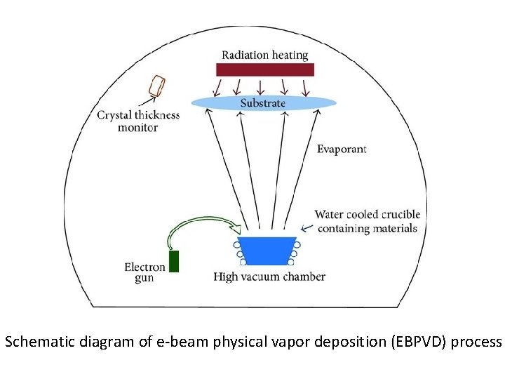
Schematic diagram of e-beam physical vapor deposition (EBPVD) process

Advantages of EBPVD It yields a high deposition rate usually from few nm/min 100’s of nm/min to from thin films at relatively low substrate temperatures, with very high material utilization efficiency. Due to the very high deposition rate, this process has potential industrial application for wear resistant and thermal barrier coatings in aerospace industries, hard coatings for cutting and tool industries, and electronic and optical films for semiconductor industries and thin film solar applications. As compared to resistive thermal evaporation or crucible heater, ebeam is capable of heating materials to much higher temperatures. Moreover, it heats a target material only, not the entire crucible resulting in a lower contamination from crucible.
Disadvantages of EBPVD is a line of sight deposition process when performed at a low enough pressure (roughly <10− 4 Torr ). The translational and rotational motion of the shaft helps for coating the outer surface of complex geometries, but this process cannot be used to coat the inner surface of complex geometries. Another potential problem is that filament degradation in the electron gun results in a nonuniform evaporation rate. However, when vapor deposition is performed at pressures of roughly 10− 4 Torr or higher, significant scattering of the vapor cloud takes place such that surfaces not in sight of the source can be coated. Strictly speaking, the slow transition from lineofsight to scattered deposition is determined not only by pressure (or mean free path) but also by source to substrate distance.
Molecular beam epitaxy (MBE) is one of several methods of depositing single crystals. It was invented in the late 1960 s at Bell Telephone Laboratories by J. R. Arthur and Alfred Y. Cho. MBE is widely used in the manufacture of semiconductor devices, including transistors for cellular phones and Wi. Fi and quantum dots etc. Molecular beam epitaxy takes place in ultrahigh vacuum (10− 10 torr) The most important aspect of MBE is the very small deposition rate (typically <1 nm/sec) allows the films to grow epitaxially. These deposition rates require proportionally better vacuum to achieve the same impurity levels as other deposition techniques. The absence of carrier gases as well as the ultra high vacuum environment result in the highest achievable purity of the grown films. Moreover ultrathin film (~1 Mono layer ) can be easily grown.
Working Mechanism MBE In solid source MBE, elements such as gallium and arsenic, in ultrapure form, are heated in separate quasi Knudsen effusion cells until they begin to slowly sublime. The gaseous elements then condense on the wafer, where they may react with each other. In the example of gallium and arsenic, single crystal gallium arsenide is formed. The term "beam" means that evaporated atoms do not interact with each other or vacuum chamber gases until they reach the wafer, due to the long mean free paths of the atoms. During operation, reflection high energy electron diffraction (RHEED) is often used for monitoring the growth of the crystal layers.
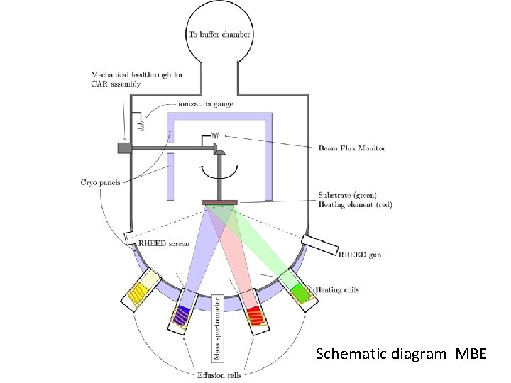
Schematic diagram MBE
Chemical Vapor Deposition (CVD) Chemical vapor deposition (CVD) is a widely used thin film coating or materials-processing technology. The majority of its applications involve applying solid thin-film coatings to surfaces, but it is also used to produce high-purity bulk materials. It has been used to deposit a very wide range of materials
Working Mechanism CVD In its simplest form, CVD involves flowing a precursor gases into a chamber containing one or more heated objects to be coated. Chemical reactions occur on and near the hot surfaces, resulting in the deposition of a thin film on the surface. This is accompanied by the production of chemical by-products that are exhausted out of the chamber along with unreacted precursor gases. Along with wide range of applications, there are many variants of CVD. It is done in hot-wall reactors and cold-wall reactors, at subtorr pressures to above-atmospheric pressures, with and without carrier gases, and at temperatures typically ranging from 2001600°C. There also a variety of enhanced CVD processes, which involve the use of plasmas, ions, photons, lasers, hot filaments, or combustion reactions to increase deposition rates and/or lower deposition temperatures.
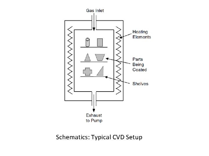
Schematics: Typical CVD Setup
Types of CVD Process There also many derivatives of the CVD terminology, such as metal-organic chemical vapor deposition (MOCVD) or organometallic chemical vapor deposition (OMCVD), which are sometimes used to note the class of molecules used in the deposition process. Some practitioners chose to differentiate epitaxial film deposition from polycrystalline or amorphous film deposition, so they introduced a variety of terms that include “epitaxy” in the acronym. Two of the more common variants are organometallic vapor phase epitaxy (OMVPE) and metalorganic vapor phase epitaxy (MOVPE) which are often used in the compound semiconductor epitaxy in literature.
Advantages of CVD Process Ø One of the primary advantages is that CVD films are generally quite conformal, i. e. , that the film thickness on the sidewalls of features is comparable to the thickness on the top. This means that films can be applied to elaborately shaped pieces, including the insides and undersides of features, and that high-aspect ratio holes and other features can be completely filled. Ø In contrast, physical vapor deposition (PVD) techniques, such as sputtering or evaporation, generally require a line-of-sight between the surface to be coated and the source. Ø Materials can be deposited with very high purity. This results from the relative ease with which impurities are removed from gaseous precursors using distillation techniques. Ø Relatively high deposition rates Ø CVD often doesn’t require as high vacuum as PVD processes.
Disadvantages of CVD Process Ø The precursors need to be volatile at near-room temperatures. This is non-trivial for a number of elements in the periodic table, although of metal-organic precursors has eased this situation. Ø CVD precursors can also be highly toxic (Ni(CO)4), explosive (B 2 H 6), or corrosive (Si. Cl 4). The byproducts of CVD reactions can also be hazardous (CO, H 2, or HF). Ø Some of these precursors, especially the metal-organic precursors, can also be quite costly. Ø The other major disadvantage is the fact that the films are usually deposited at elevated temperatures. This puts some restrictions on the kind of substrates that can be coated. More importantly, it leads to stresses in films deposited on materials with different thermal expansion coefficients, which can cause mechanical instabilities in the deposited films.
- Slides: 13