Electron Beam Lithography EBL for HighVolume Manufacturing Paul
Electron Beam Lithography (EBL) for High-Volume Manufacturing Paul Meyer October 10, 2017

PSA! • Remember to bring handouts 1
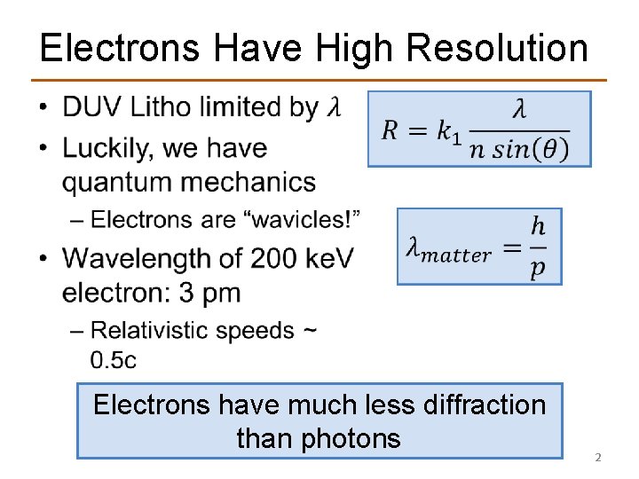
Electrons Have High Resolution • Electrons have much less diffraction than photons 2
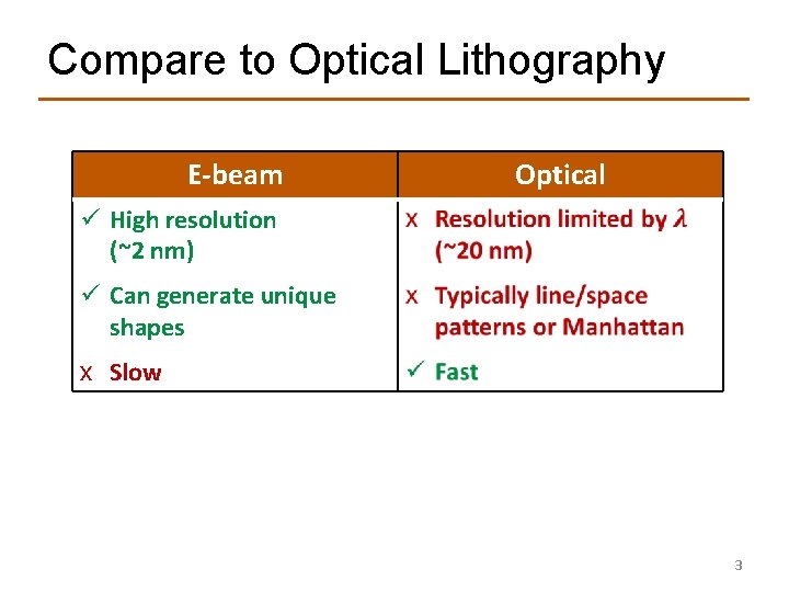
Compare to Optical Lithography E-beam Optical ü High resolution (~2 nm) ü Can generate unique shapes x Slow 3
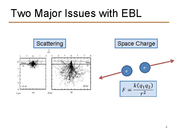
Two Major Issues with EBL Scattering Space Charge e- e- 4
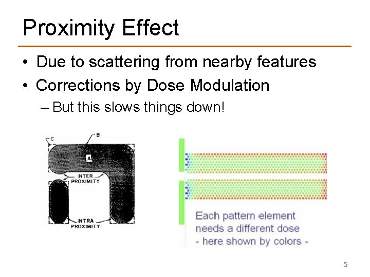
Proximity Effect • Due to scattering from nearby features • Corrections by Dose Modulation – But this slows things down! 5
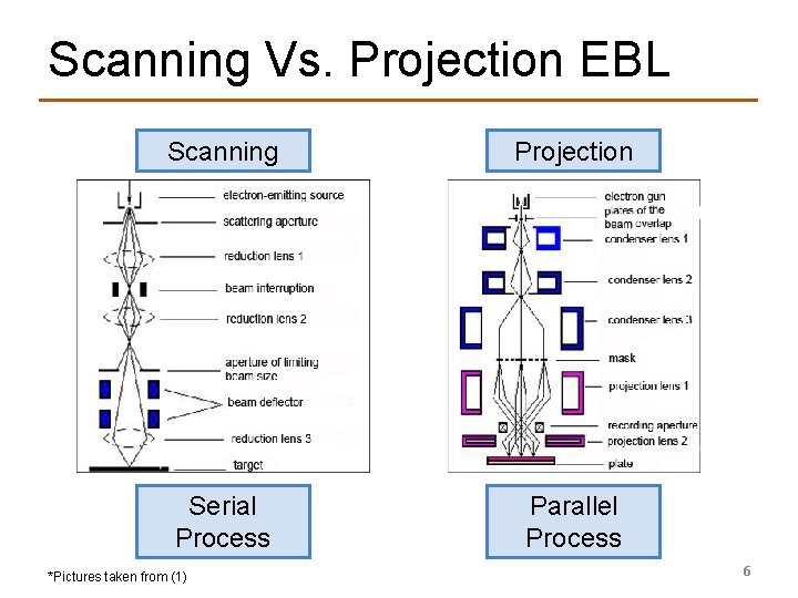
Scanning Vs. Projection EBL Scanning Projection Serial Process Parallel Process *Pictures taken from (1) 6
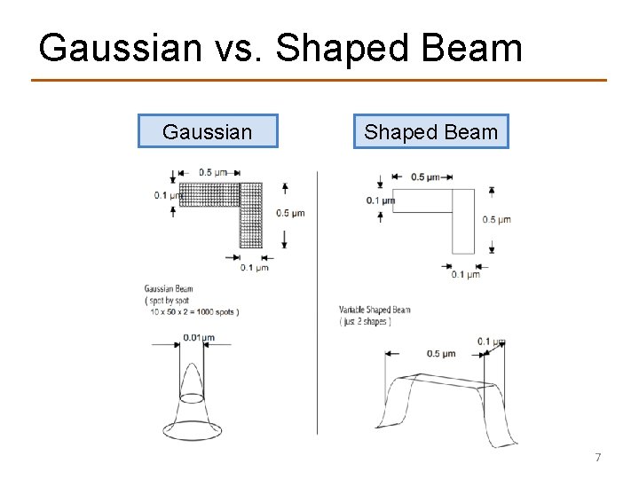
Gaussian vs. Shaped Beam Gaussian Shaped Beam 7
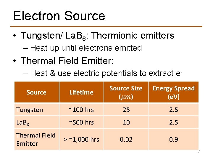
Electron Source • Tungsten/ La. B 6: Thermionic emitters – Heat up until electrons emitted • Thermal Field Emitter: – Heat & use electric potentials to extract e. Source Energy Spread (e. V) Lifetime Tungsten ~100 hrs 25 2. 5 La. B 6 ~500 hrs 10 2. 5 > ~1, 000 hrs 0. 02 0. 9 Thermal Field Emitter 8
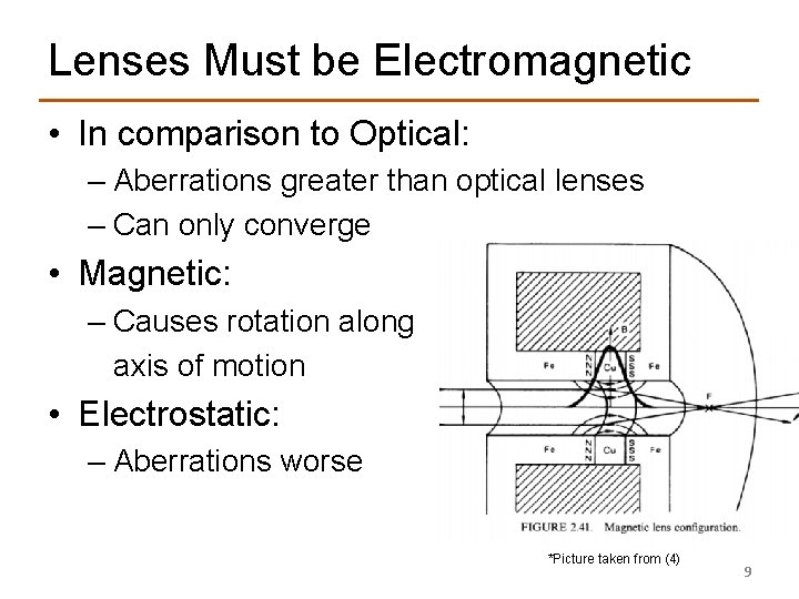
Lenses Must be Electromagnetic • In comparison to Optical: – Aberrations greater than optical lenses – Can only converge • Magnetic: – Causes rotation along axis of motion • Electrostatic: – Aberrations worse *Picture taken from (4) 9
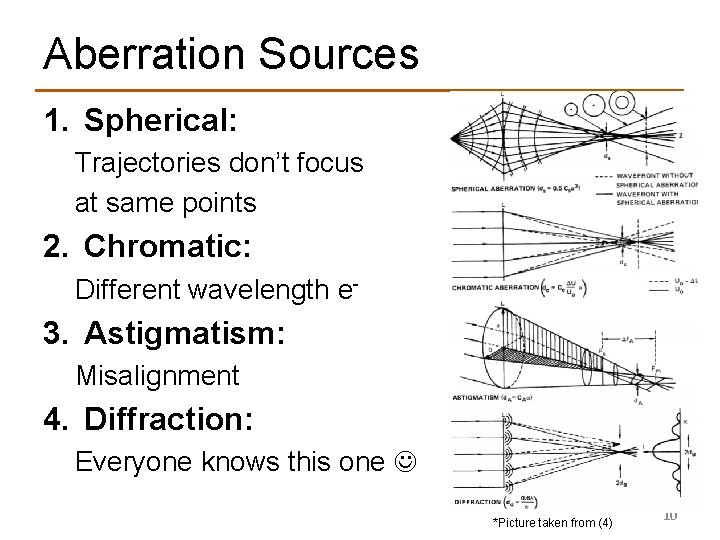
Aberration Sources 1. Spherical: Trajectories don’t focus at same points 2. Chromatic: Different wavelength e- 3. Astigmatism: Misalignment 4. Diffraction: Everyone knows this one *Picture taken from (4) 10
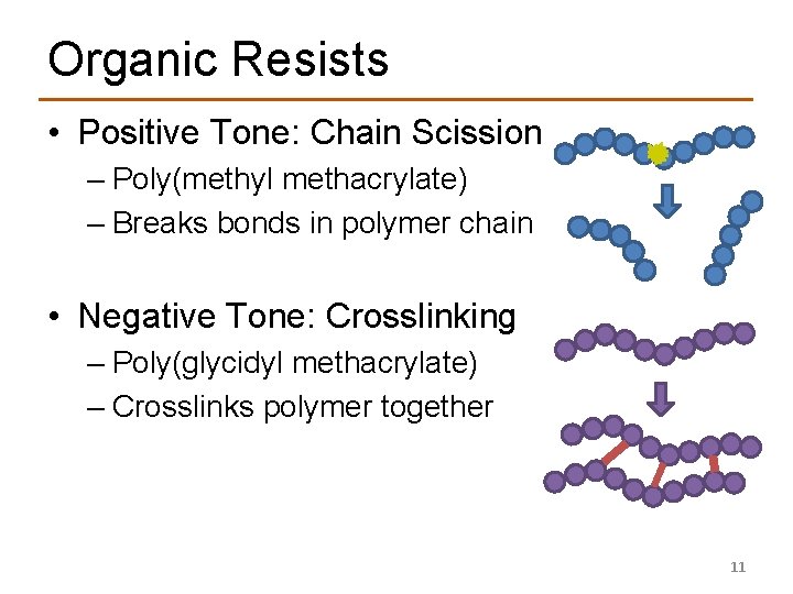
Organic Resists • Positive Tone: Chain Scission – Poly(methyl methacrylate) – Breaks bonds in polymer chain • Negative Tone: Crosslinking – Poly(glycidyl methacrylate) – Crosslinks polymer together 11
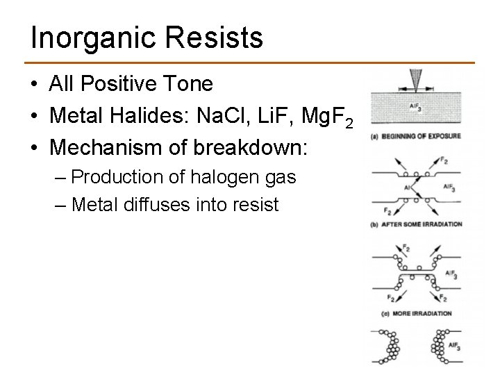
Inorganic Resists • All Positive Tone • Metal Halides: Na. Cl, Li. F, Mg. F 2 • Mechanism of breakdown: – Production of halogen gas – Metal diffuses into resist 12
Attempts at High-Volume E-Beam Lithography
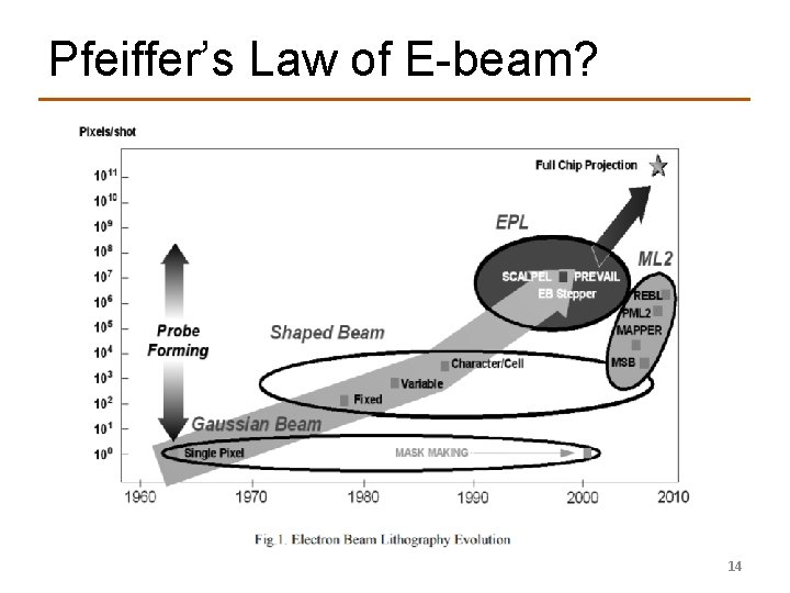
Pfeiffer’s Law of E-beam? 14
Electron Beam Exposure System (EBES) • First commercial e-beam tool – ~1960’s • Gaussian beam system • Exposed one pixel at a time • Eventually used to make photomasks 15
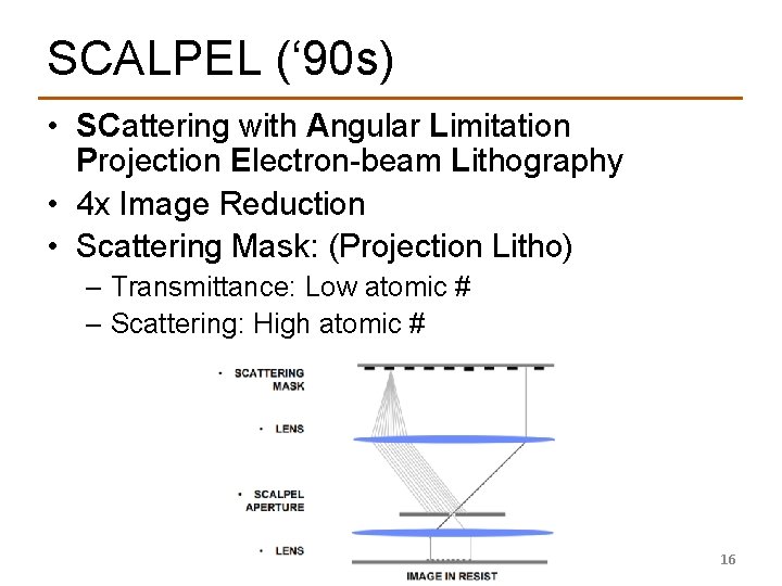
SCALPEL (‘ 90 s) • SCattering with Angular Limitation Projection Electron-beam Lithography • 4 x Image Reduction • Scattering Mask: (Projection Litho) – Transmittance: Low atomic # – Scattering: High atomic # 16
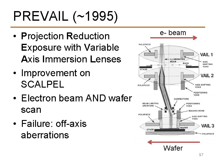
PREVAIL (~1995) • Projection Reduction Exposure with Variable Axis Immersion Lenses • Improvement on SCALPEL • Electron beam AND wafer scan • Failure: off-axis aberrations e- beam Wafer 17
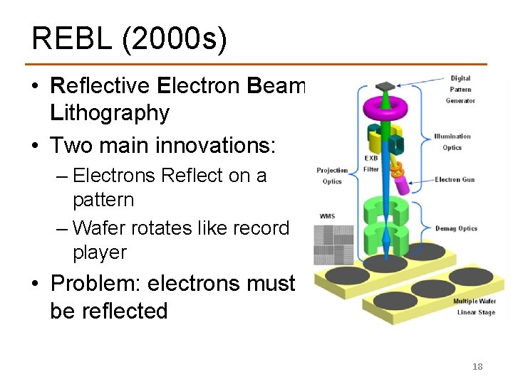
REBL (2000 s) • Reflective Electron Beam Lithography • Two main innovations: – Electrons Reflect on a pattern – Wafer rotates like record player • Problem: electrons must be reflected 18
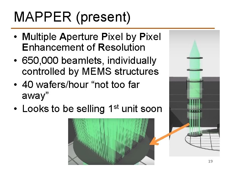
MAPPER (present) • Multiple Aperture Pixel by Pixel Enhancement of Resolution • 650, 000 beamlets, individually controlled by MEMS structures • 40 wafers/hour “not too far away” • Looks to be selling 1 st unit soon 19
MAPPER Cont. • Epilepsy Warning: • https: //youtu. be/mof. JPqlc. Rz 0? t=107 20
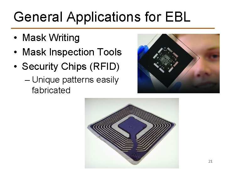
General Applications for EBL • Mask Writing • Mask Inspection Tools • Security Chips (RFID) – Unique patterns easily fabricated 21
Summary • Many attempts made for high-volume manufacturing; none succeeded (so far) • E-beam lithography is useful for: – Complex, small patterns (not line/space) – Low throughput, high resolution • Limitations come from: – Aberrations in lenses – Scattering – Proximity Effects – Space Charge 22
Thank you for Listening! • Questions? 23
References 1. 2. 3. 4. 5. 6. 7. http: //eng. thesaurus. rusnano. com/wiki/article 1093 SPIE Handbook, Volume 1: Microlithography, Section 2. 3 http: //www. cnf. cornell. edu/cnf_spie 3. html (accessed Oct 8, 2017). Electron Beam Lithography. Stephan Kapfinger. January 26, 2009. Technische Universität München. E-Beam Lithography “The Physics of Micro/Nano-Fabrication. ” Ivor Brodie, Julius Muray. Vistec Shaped Beam Technology. Ines Stolberg. Mc. Cord, M. A. ; Petric, P. ; Ummethala, U. ; Carroll, A. ; Kojima, S. ; Grella, L. ; Shriyan, S. ; Rettner, C. T. & Bevis, C. F. ; “REBL: design progress toward 16 nm half-pitch maskless projection electron beam lithography”, Proc. SPIE, 2012 Harriott, L. R. SCALPEL: Projection Electron Beam Lithography. Proc. 1999 Part. Accel. Conf. (Cat. No. 99 CH 36366) 1999, 1, 595– 599 DOI: 10. 1109/PAC. 1999. 795770. Disclaimer: All pictures were taken from other sources and are not my own 24
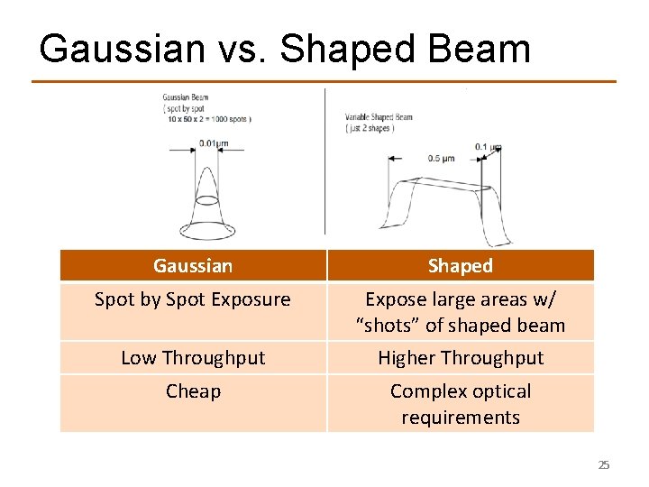
Gaussian vs. Shaped Beam Gaussian Shaped Spot by Spot Exposure Expose large areas w/ “shots” of shaped beam Higher Throughput Low Throughput Cheap Complex optical requirements 25
- Slides: 26