ELECTROMAGNETIC 3 D SOLVER TOOL OF CHOICE FOR
- Slides: 19


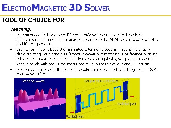
ELECTROMAGNETIC 3 D SOLVER TOOL OF CHOICE FOR Teaching: • • recommended for Microwave, RF and mm. Wave (theory and circuit design), Electromagnetic Theory, Electromagnetic compatibility, MEMS design courses, MMIC and IC design course easy to learn (complete set of animated tutorials), create animations (AVI, GIF) demonstrating basic principles (standing waves and matching, interference, working principles of a component), competitive prices for equipping complete classrooms keep in touch with one of the most used tools in the Microwave and RF industry seamlessly interfaced with the most popular microwave & circuit design suite: AWR Microwave Office Standing waves Coupler 800 -1200 MHz Isolated port Excited port

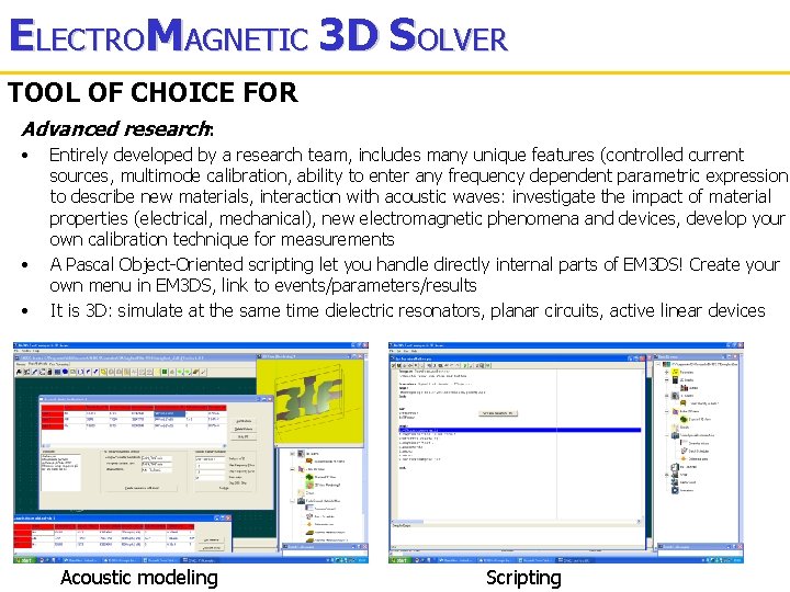
ELECTROMAGNETIC 3 D SOLVER TOOL OF CHOICE FOR Advanced research: • • • Entirely developed by a research team, includes many unique features (controlled current sources, multimode calibration, ability to enter any frequency dependent parametric expression to describe new materials, interaction with acoustic waves: investigate the impact of material properties (electrical, mechanical), new electromagnetic phenomena and devices, develop your own calibration technique for measurements A Pascal Object-Oriented scripting let you handle directly internal parts of EM 3 DS! Create your own menu in EM 3 DS, link to events/parameters/results It is 3 D: simulate at the same time dielectric resonators, planar circuits, active linear devices Acoustic modeling Scripting

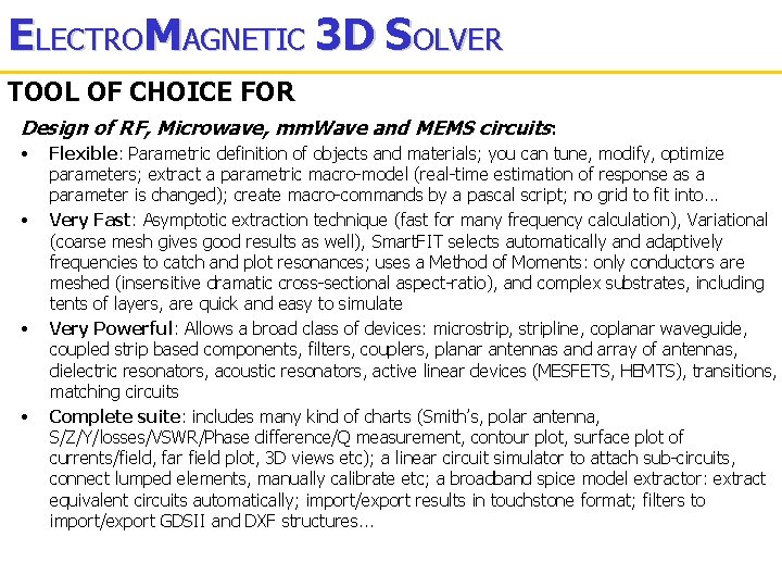
ELECTROMAGNETIC 3 D SOLVER TOOL OF CHOICE FOR Design of RF, Microwave, mm. Wave and MEMS circuits: • • Flexible: Parametric definition of objects and materials; you can tune, modify, optimize parameters; extract a parametric macro-model (real-time estimation of response as a parameter is changed); create macro-commands by a pascal script; no grid to fit into. . . Very Fast: Asymptotic extraction technique (fast for many frequency calculation), Variational (coarse mesh gives good results as well), Smart. FIT selects automatically and adaptively frequencies to catch and plot resonances; uses a Method of Moments: only conductors are meshed (insensitive dramatic cross-sectional aspect-ratio), and complex substrates, including tents of layers, are quick and easy to simulate Very Powerful: Allows a broad class of devices: microstrip, stripline, coplanar waveguide, coupled strip based components, filters, couplers, planar antennas and array of antennas, dielectric resonators, acoustic resonators, active linear devices (MESFETS, HEMTS), transitions, matching circuits Complete suite: includes many kind of charts (Smith’s, polar antenna, S/Z/Y/losses/VSWR/Phase difference/Q measurement, contour plot, surface plot of currents/field, far field plot, 3 D views etc); a linear circuit simulator to attach sub-circuits, connect lumped elements, manually calibrate etc; a broadband spice model extractor: extract equivalent circuits automatically; import/export results in touchstone format; filters to import/export GDSII and DXF structures. . .

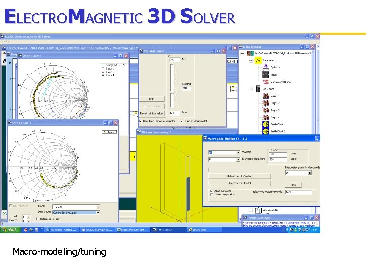
ELECTROMAGNETIC 3 D SOLVER Macro-modeling/tuning

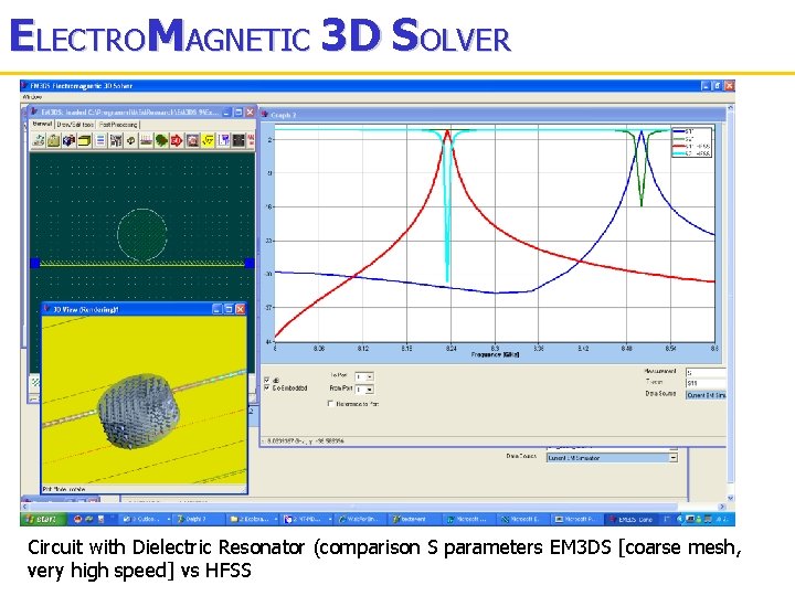
ELECTROMAGNETIC 3 D SOLVER Circuit with Dielectric Resonator (comparison S parameters EM 3 DS [coarse mesh, very high speed] vs HFSS

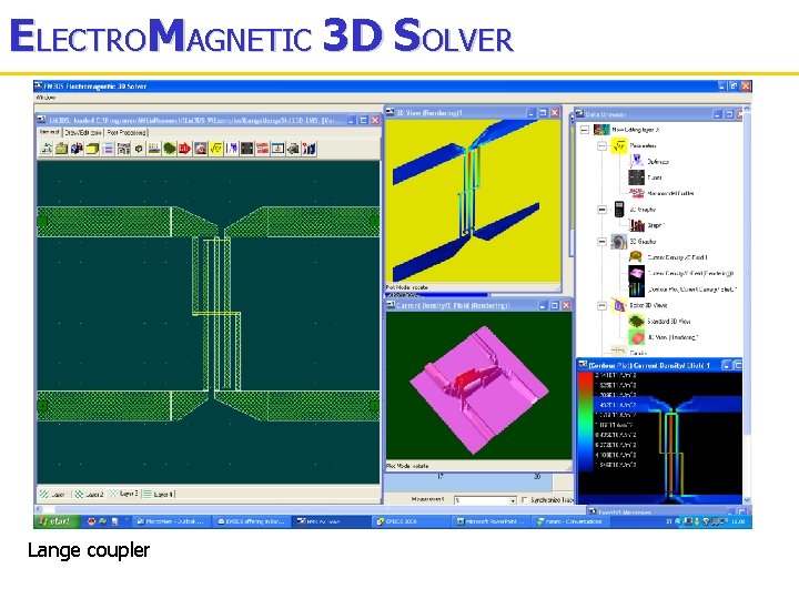
ELECTROMAGNETIC 3 D SOLVER Lange coupler

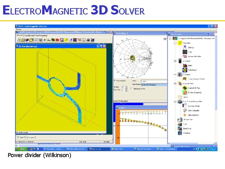
ELECTROMAGNETIC 3 D SOLVER Power divider (Wilkinson)

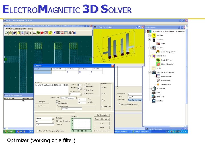
ELECTROMAGNETIC 3 D SOLVER Optimizer (working on a filter)

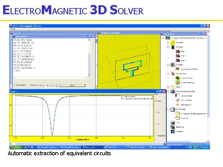
ELECTROMAGNETIC 3 D SOLVER Automatic extraction of equivalent circuits

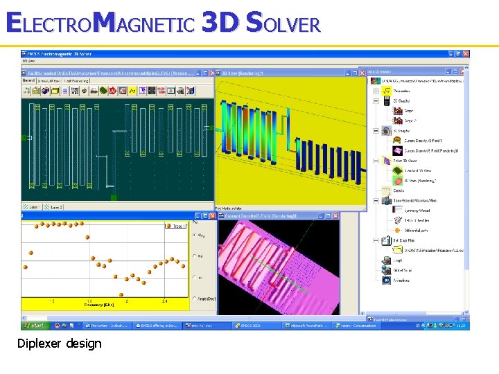
ELECTROMAGNETIC 3 D SOLVER Diplexer design

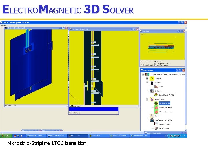
ELECTROMAGNETIC 3 D SOLVER Microstrip-Stripline LTCC transition

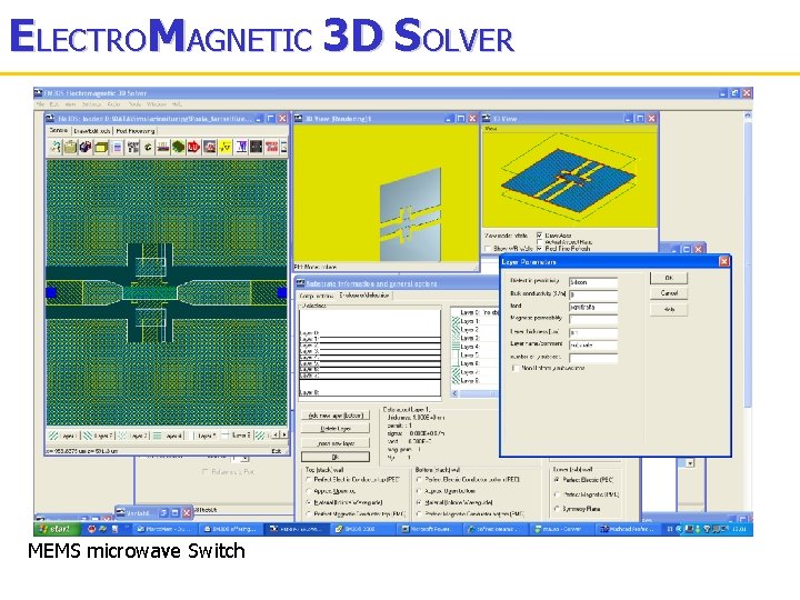
ELECTROMAGNETIC 3 D SOLVER MEMS microwave Switch

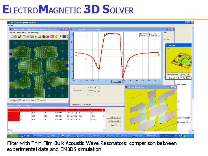
ELECTROMAGNETIC 3 D SOLVER Filter with Thin Film Bulk Acoustic Wave Resonators: comparison between experimental data and EM 3 DS simulation

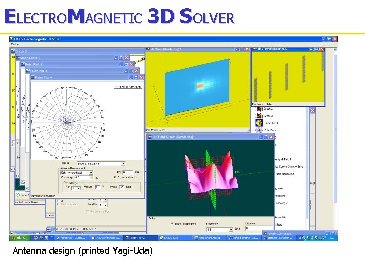
ELECTROMAGNETIC 3 D SOLVER Antenna design (printed Yagi-Uda)

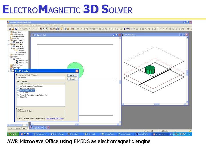
ELECTROMAGNETIC 3 D SOLVER AWR Microwave Office using EM 3 DS as electromagnetic engine

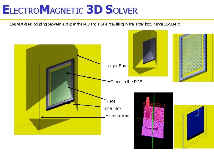
ELECTROMAGNETIC 3 D SOLVER EMI test case: coupling between a strip in the PCB and a wire travelling in the larger box. Range 10 -50 MHz Larger Box Trace in the PCB FR 4 Inner Box External wire

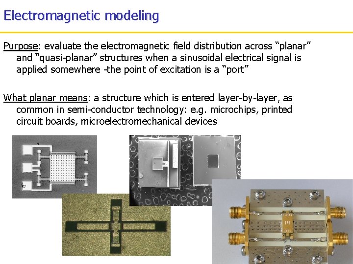
Electromagnetic modeling Purpose: evaluate the electromagnetic field distribution across “planar” and “quasi-planar” structures when a sinusoidal electrical signal is applied somewhere -the point of excitation is a “port” What planar means: a structure which is entered layer-by-layer, as common in semi-conductor technology: e. g. microchips, printed circuit boards, microelectromechanical devices

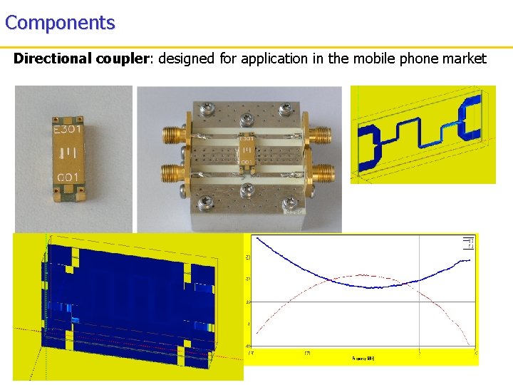
Components Directional coupler: designed for application in the mobile phone market