ELECTROCHEMICAL IMPEDANCE SPECTROSCOPY EIS A TOOL FOR THE


- Slides: 31

ELECTROCHEMICAL IMPEDANCE SPECTROSCOPY (EIS): A TOOL FOR THE CHARACTERIZATION OF SPUTTERED NIOBIUM FILMS M. Musiani Istituto per l’Energetica e le Interfasi, CNR, C. so Stati Uniti 4, 35127 Padova, Italy Work performed in collaboration with V. Palmieri, D. Tonini (INFN LNL) and with S. Cattarin (IENI CNR)

Contents Electrochemical Impedance Spectroscopy (EIS) EIS, Capacity and Surface Roughness EIS of porous/rough electrodes Magnetron Sputtering of Nb EIS results: - Surface roughness as a function of Target-Substrate angle - Attempts to control surface roughness Conclusions

Part 1 Electrochemical Impedance Spectroscopy

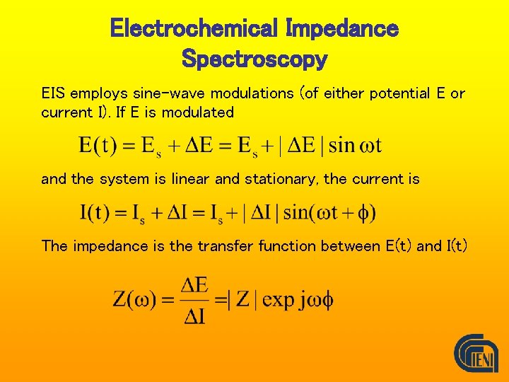
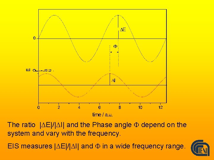
Electrochemical Impedance Spectroscopy EIS employs sine-wave modulations (of either potential E or current I). If E is modulated and the system is linear and stationary, the current is The impedance is the transfer function between E(t) and I(t)

The ratio |DE|/|DI| and the Phase angle F depend on the system and vary with the frequency. EIS measures |DE|/|DI| and F in a wide frequency range.

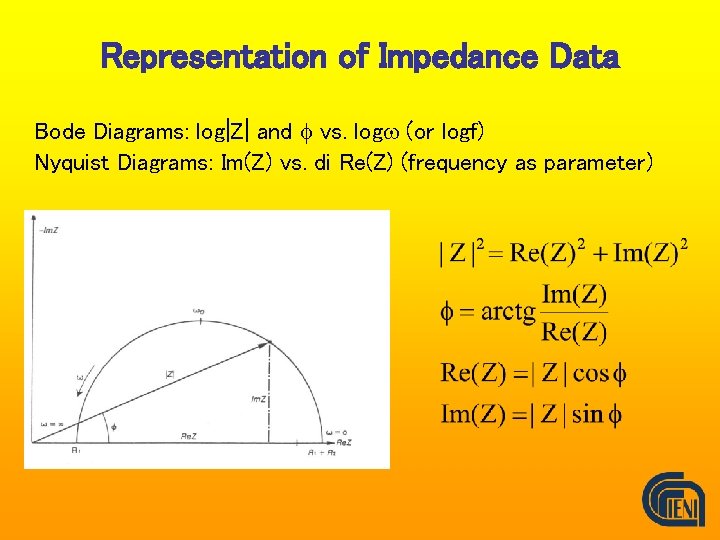
Representation of Impedance Data Bode Diagrams: log|Z| and f vs. logw (or logf) Nyquist Diagrams: Im(Z) vs. di Re(Z) (frequency as parameter)

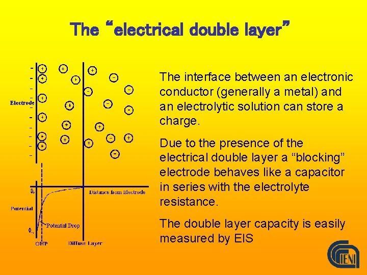
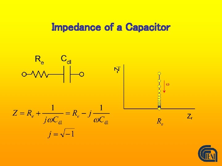
The “electrical double layer” The interface between an electronic conductor (generally a metal) and an electrolytic solution can store a charge. Due to the presence of the electrical double layer a “blocking” electrode behaves like a capacitor in series with the electrolyte resistance. The double layer capacity is easily measured by EIS

Impedance of a Capacitor

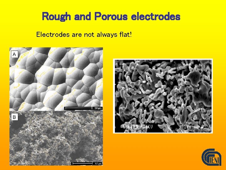
Rough and Porous electrodes Electrodes are not always flat!

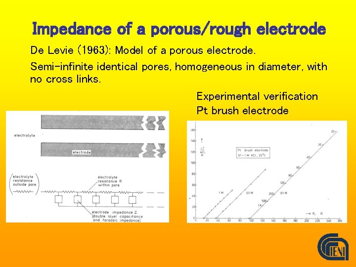
Impedance of a porous/rough electrode De Levie (1963): Model of a porous electrode. Semi-infinite identical pores, homogeneous in diameter, with no cross links. Experimental verification Pt brush electrode

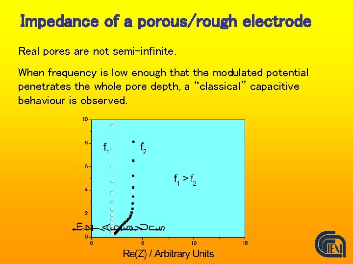
Impedance of a porous/rough electrode Real pores are not semi-infinite. When frequency is low enough that the modulated potential penetrates the whole pore depth, a “classical” capacitive behaviour is observed.

Impedance of a porous/rough electrode Keddam et al. (1981) “When a porous electrode is constituted of a three dimensional combination of small occluded pore units, the electrode impedance becomes very similar to that of a cylindrical pore electrode” Keddam et al. (1982) “At sufficiently low frequency, the impedance of a cylindrical pore is equal to that of the flat electrode of the same area as the developed pore surface”

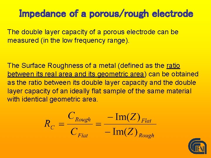
Impedance of a porous/rough electrode The double layer capacity of a porous electrode can be measured (in the low frequency range). The Surface Roughness of a metal (defined as the ratio between its real area and its geometric area) can be obtained as the ratio between its double layer capacity and the double layer capacity of an ideally flat sample of the same material with identical geometric area.

Part 2 Magnetron Sputtering of Nb

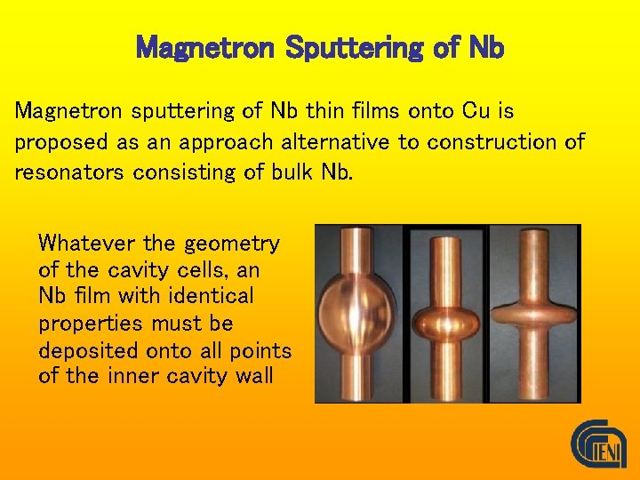
Magnetron Sputtering of Nb Magnetron sputtering of Nb thin films onto Cu is proposed as an approach alternative to construction of resonators consisting of bulk Nb. Whatever the geometry of the cavity cells, an Nb film with identical properties must be deposited onto all points of the inner cavity wall

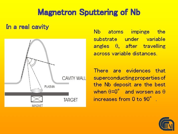
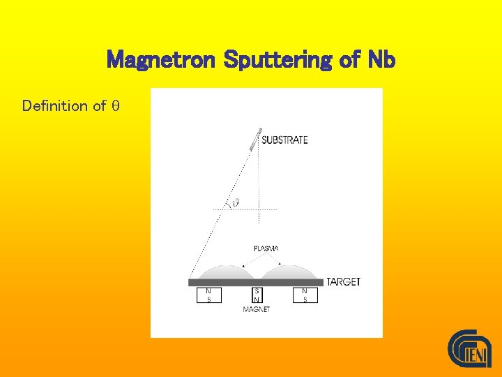
Magnetron Sputtering of Nb In a real cavity Nb atoms impinge the substrate under variable angles q, after travelling across variable distances. There are evidences that superconducting properties of the Nb deposit are the best when q=0° and worsen as q increases from 0 to 90°.

Magnetron Sputtering of Nb Definition of q

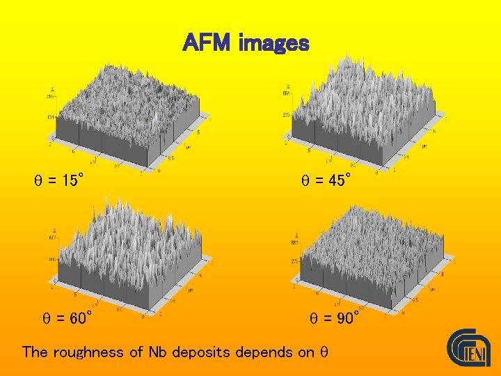
AFM images q = 15° q = 60° q = 45° q = 90° The roughness of Nb deposits depends on q

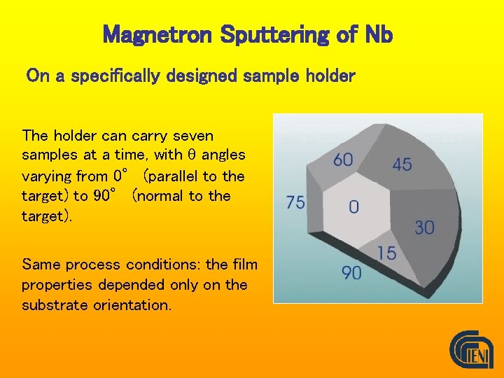
Magnetron Sputtering of Nb On a specifically designed sample holder The holder can carry seven samples at a time, with q angles varying from 0° (parallel to the target) to 90° (normal to the target). Same process conditions: the film properties depended only on the substrate orientation.

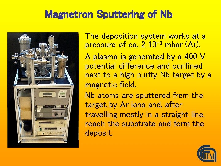
Magnetron Sputtering of Nb The deposition system works at a pressure of ca. 2 10 -3 mbar (Ar). A plasma is generated by a 400 V potential difference and confined next to a high purity Nb target by a magnetic field. Nb atoms are sputtered from the target by Ar ions and, after travelling mostly in a straight line, reach the substrate and form the deposit.

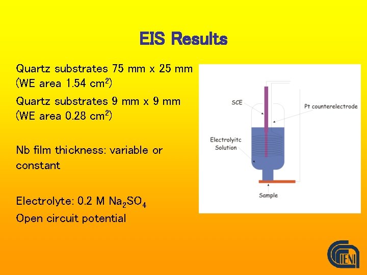
EIS Results Quartz substrates 75 mm x 25 mm (WE area 1. 54 cm 2) Quartz substrates 9 mm x 9 mm (WE area 0. 28 cm 2) Nb film thickness: variable or constant Electrolyte: 0. 2 M Na 2 SO 4 Open circuit potential

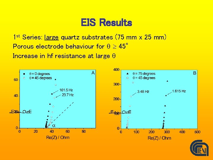
EIS Results 1 st Series: large quartz substrates (75 mm x 25 mm) Porous electrode behaviour for q 45° Increase in hf resistance at large q

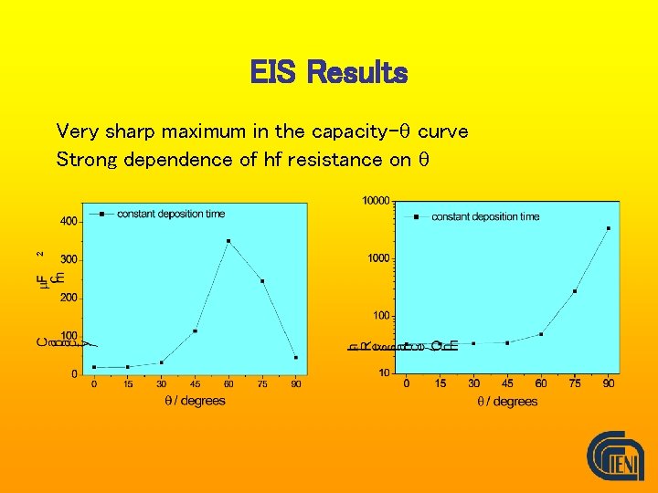
EIS Results Very sharp maximum in the capacity-q curve Strong dependence of hf resistance on q

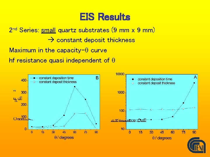
EIS Results 2 nd Series: small quartz substrates (9 mm x 9 mm) constant deposit thickness Maximum in the capacity-q curve hf resistance quasi independent of q

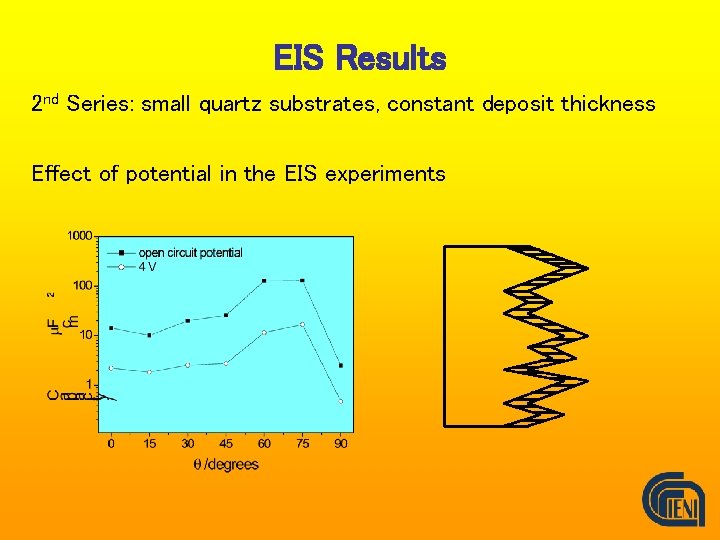
EIS Results 2 nd Series: small quartz substrates, constant deposit thickness Effect of potential in the EIS experiments

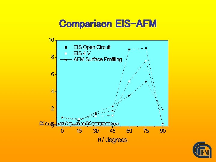
Comparison EIS-AFM

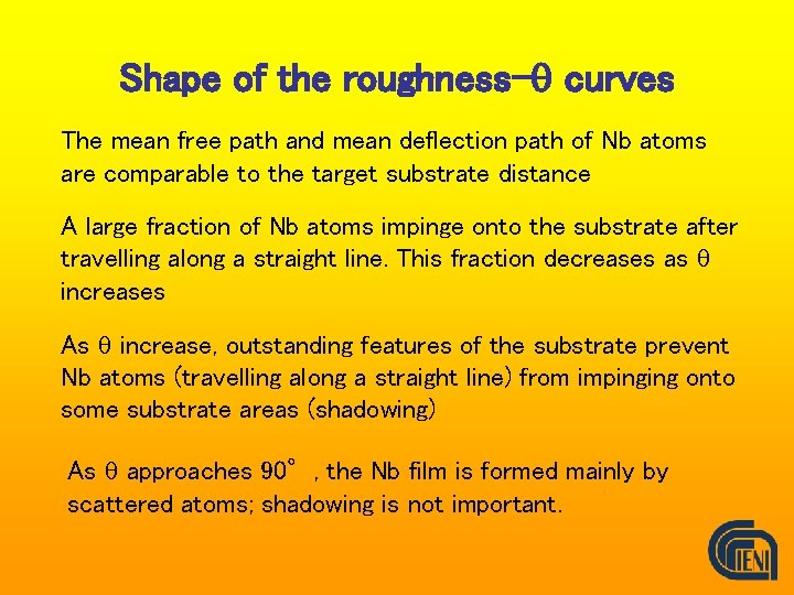
Shape of the roughness-q curves The mean free path and mean deflection path of Nb atoms are comparable to the target substrate distance A large fraction of Nb atoms impinge onto the substrate after travelling along a straight line. This fraction decreases as q increases As q increase, outstanding features of the substrate prevent Nb atoms (travelling along a straight line) from impinging onto some substrate areas (shadowing) As q approaches 90°, the Nb film is formed mainly by scattered atoms; shadowing is not important.

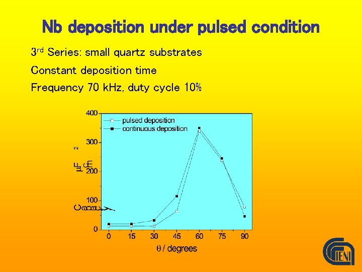
Nb deposition under pulsed condition 3 rd Series: small quartz substrates Constant deposition time Frequency 70 k. Hz, duty cycle 10%

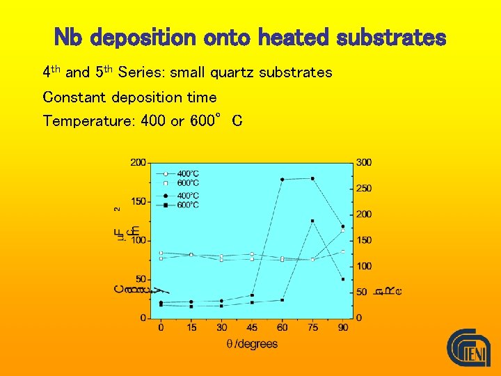
Nb deposition onto heated substrates 4 th and 5 th Series: small quartz substrates Constant deposition time Temperature: 400 or 600°C

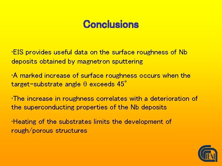
Conclusions • EIS provides useful data on the surface roughness of Nb deposits obtained by magnetron sputtering • A marked increase of surface roughness occurs when the target-substrate angle q exceeds 45° • The increase in roughness correlates with a deterioration of the superconducting properties of the Nb deposits • Heating of the substrates limits the development of rough/porous structures

Thanks for your attention