Electrical Engineering Materials EE 3219 Dr Md Sherajul


 and")


")


 Solids are composed of randomly orientated atoms, ions, or")


 Lattice with Different Choices for the Basis")


![Significance of Crystallographic Directions It is much easier to magnetize iron in the [100]](https://slidetodoc.com/presentation_image_h/37cee60d5516976cab83b2c659257874/image-53.jpg "Significance of Crystallographic Directions It is much easier to magnetize iron in the [100]")


- Slides: 63
Electrical Engineering Materials EE 3219 Dr. Md. Sherajul Islam Department of Electrical and Electronic Engineering Khulna University of Engineering & Technology Khulna, Bangladesh
LECTURE - 1 Elementary Materials Science Concepts
UNIVERSE HYPERBOLIC EUCLIDEAN SPHERICAL STRONG WEAK ELECTROMAGNET ENERGY SPACE GRAVITY n. D + t FIELDS PARTICLES METAL SEMI-METAL BAND STRUCTURE NON-ATOMIC SEMI-CONDUCTOR INSULATOR STATE / VISCOSITY GAS SOLID LIQUID CRYSTALS LIQUID STRUCTURE AMORPHOUS QUASICRYSTALS RATIONAL APPROXIMANTS CRYSTALS SIZE NANO-QUASICRYSTALS NANOCRYSTALS
Solids • Solids consist of atoms or molecules undergoing thermal motion about their equilibrium positions, which are at fixed points in space. STRUCTURE OF SOLIDS q Types of solids based on structure q Types of solids based on bonding
Bonding and Types of Solids
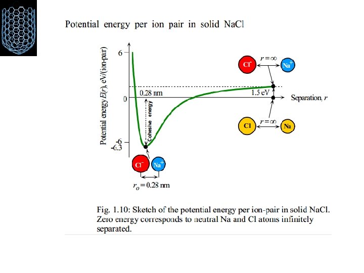
Bonding Energies and Forces Potential Energy, E repulsion 0 attraction equilibrium Typical potential between two atoms Repulsion when they are brought close together Related to Pauli principle (As electron clouds overlap energy increases) Attractive part: at large distances (Depends on type of bonding)
• This typical curve has a minimum at equilibrium distance R 0 • R > R 0 ; – the potential increases gradually, approaching 0 as R ∞ – the force is attractive • R < R 0; – the potential increases very rapidly, approaching ∞ at small separation. – the force is repulsive V(R) Repulsive 0 R Attractive r R ¡Force between the atoms is the negative of the slope of this curve. At equlibrium, repulsive force becomes equals to the attractive part.
The potential energy of either atom will be given by: V= decrease in potential energy+increase in potential energy (due to attraction) (due to repulsion) or simply: V(r): the net potential energy of interaction as function of r r : the distance between atoms, ions, or molecules a, b: proportionality constant of attraction and repulsion, respectively m, n: constant characteristics of each type of bond and type of structure
• Primary Bonds Ionic Covalent Metallic • Secondary Bonding Van der Waals Hydrogen bond • Molecules and Molecular Solids
1 - IONIC BONDING Ionic bonding is the electrostatic force of attraction between positively and negatively charged ions (between non-metals and metals). These ions have been produced as a result of a transfer of electrons between two atoms with a large difference in electro negativities. All ionic compounds are crystalline solids at room temperature. Na. Cl is a typical example of ionic bonding.
• The metallic elements have only up to the valence electrons in their outer shell will lose their electrons and become positive ions, whereas electronegative elements tend to acquire additional electrons to complete their octed and become negative ions, or anions. Na Cl
Na. Cl • Notice that when sodium loses its one valence electron it gets smaller in size, while chlorine grows larger when it gains an additional valance electron. After the reaction takes place, the charged Na+ and Cl- ions are held together by electrostatic forces, thus forming an ionic bond.
• When the Na+ and Cl- ions approach each other closely enough so that the orbits of the electron in the ions begin the overlap each other, then the electron begins to repel each other by virtue of the repulsive electrostatic coulomb force. Of course the closer together the ions are, the grater the repulsive force. • Pauli exclusion principle has an important role in repulsive force. To prevent a violation of the exclusion principle, the potential energy of the system increases very rapidly.
Property Explanation Melting point and boiling point The melting and boiling points of ionic compounds are high because a large amount of thermal energy is required to separate the ions which are bound by strong electrical forces. Electrical conductivity Solid ionic compounds do not conduct electricity when a potential is applied because there are no mobile charged particles. No free electrons causes the ions to be firmly bound and cannot carry charge by moving. Hardness Most ionic compounds are hard; the surfaces of their crystals are not easily scratches. This is because the ions are bound strongly to the lattice and aren't easily displaced. Brittleness Most ionic compounds are brittle; a crystal will shatter if we try to distort it. This happens because distortion cause ions of like charges to come close together then sharply repel.
2 - COVALENT BONDING • Covalent bonding takes place between atoms with small differences in electronegativity which are close to each other in periodic table (between non-metals and nonmetals). • The covalent bonding is formed by sharing of outer shell electrons (i. e. , s and p electrons) between atoms rather than by electron transfer. • This bonding can be attained if the two atoms each share one of the other’s electrons. • So the noble gas electron configuration can be attained.
• Each electron in a shared pair is attracted to both nuclei involved in the bond. The approach, electron overlap, and attraction can be visualized as shown in the following figure representing the nuclei and electrons in a hydrogen molecule. e e
Property Explanation Melting point and boiling point Very high melting points because each atom is bound by strong covalent bonds. Many covalent bonds must be broken if the solid is to be melted and a large amount of thermal energy is required for this. Electrical conductivity Poor conductors because electrons are held either on the atoms or within covalent bonds. They cannot move through the lattice. Hardness Brittleness They are hard because the atoms are strongly bound in the lattice, and are not easily displaced. Covalent network substances are brittle. If sufficient force is applied to a crystal, covalent bond are broken as the lattice is distorted. Shattering occurs rather than deformation of a shape.
Comparison of Ionic and Covalent Bonding
3 - METALLIC BONDING • Metallic bonding is the type of bonding found in metal elements. This is the electrostatic force of attraction between positively charged ions and delocalized outer electrons. • The metallic bond is weaker than the ionic and the covalent bonds. Metallic bonding is the force of attraction between valence electrons and the metal ions. It is the sharing of many detached electrons between many positive ions, where the electrons act as a "glue" giving the substance a definite structure.
METALLIC BONDING • Metallic structures are typically rather empty (having large internuclear spacings) and prefer lattice arrangements in which each atom has many nearest neighbors. • The weakness of the individual bonding actions in a metal is due to the enlargement of the internuclear spacing.
v Valance electrons are relatively bound to the nucleus and therefore they move freely through the metal and they are spread out among the atoms in the form of a low-density electron cloud. v. A metallic bond result from the sharing of a variable number of electrons by a variable number of v atoms. A metal may be described as a cloud of free electrons. v Therefore, metals have high electrical and thermal conductivity. + + + + +
• All valence electrons in a metal combine to form a “sea” of electrons that move freely between the atom cores. The more electrons, the stronger the attraction. This means the melting and boiling points are higher, and the metal is stronger and harder. • The positively charged cores are held together by these negatively charged electrons. • The free electrons act as the bond (or as a “glue”) between the positively charged ions. • This type of bonding is nondirectional and is rather insensitive to structure. • As a result we have a high ductility of metals - the “bonds” do not “break” when atoms are rearranged – metals can experience a significant degree of plastic deformation.
4 - VAN DER WAALS BONDING • It is a weak bond, with a typical strength of 0. 2 e. V/atom. • It occurs between neutral atoms and molecules. • The explanation of these weak forces of attraction is that there are natural fluctuation in the electron density of all molecules and these cause small temporary dipoles within the molecules. It is these temporary dipoles that attract one molecule to another. They are called van der Waals' forces. • The bigger a molecule is, the easier it is to polarise (to form a dipole), and so the van der Waal's forces get stronger, so bigger molecules exist as liquids or solids rather than gases.
• The shape of a molecule influences its ability to form temporary dipoles. Long thin molecules can pack closer to each other than molecules that are more spherical. The bigger the 'surface area' of a molecule, the greater the van der Waal's forces will be and the higher the melting and boiling points of the compound will be. • Van der Waal's forces are of the order of 1% of the strength of a covalent bond. Homonuclear molecules, such as iodine, develop temporary dipoles due to natural fluctuations of electron density within the molecule Heteronuclear molecules, such as H-Cl have permanent dipoles that attract the opposite pole in other molecules.
The dipoles can be formed as a result of unbalanced distribution of electrons in asymettrical molecules. This is caused by the instantaneous location of a few more electrons on one side of the nucleus than on the other. symmetric asymmetric Therefore atoms or molecules containing dipoles are attracted to each other by electrostatic forces. Display a marked attractive forces No attraction is produced
• These forces are due to the electrostatic attraction between the nucleus of one atom and the electrons of the other. ¡ Van der waals interaction occurs generally between atoms which have noble gas configuration. van der waals bonding
5 – HYDROGEN BONDING • A hydrogen atom, having one electron, can be covalently bonded to only one atom. However, the hydrogen atom can involve itself in an additional electrostatic bond with a second atom of highly electronegative character such as fluorine or oxygen. This second bond permits a hydrogen bond between two atoms or strucures. • The strength of hydrogen bonding varies from 0. 1 to 0. 5 ev/atom. n Hydrogen bonds connect water molecules in ordinary ice. Hydrogen bonding is also very important in proteins and nucleic acids and therefore in life processes.
¡Types ¡Ionic ¡Van Der Waals ¡ Bonding ¡Bonding of Bonding ¡Metallic ¡ Bonding ¡Covalent ¡Hydrogen Bonding ¡ ¡Low ¡ ¡High Melting Point ¡Hard Low Melting Points ¡ ¡ and Brittle conducting ¡ solid ¡Na. Cl, Cs. Cl, Zn. S Melting ¡Point Very High Melting ¡ Point ¡ Soft and Brittle ¡Variable ¡ ¡Non ¡Variable Non-Conducting ¡ ¡Hardness ¡ ¡ Ne, Ar, Kr and Xe Very Hard ¡Conducting ¡Fe, Cu, Ag ¡ ¡ Usually not Conducting Diamond, Graphite Melting Points ¡Soft and Brittle ¡Usually ¡Non-Conducting ¡İce, ¡organic solids
Periodic Arrays of Atoms Experimental Evidence of periodic structures. (See Kittel, Fig. 1. ) The external appearance of crystals gives some clues to this. Fig. 1 shows that when a crystal is cleaved, we can see that it is built up of identical “building blocks”. Further, the early crystallographers noted that the index numbers that define plane orientations are exact integers. Cleaving a Crystal
Elementary Crystallography Solid Material Types Crystalline Single Crystals Polycrystalline Amorphous
Crystalline Solids • A Crystalline Solid is the solid form of a substance in which the atoms or molecules are arranged in a definite, repeating pattern in three dimensions. • Single Crystals, ideally have a high degree of order, or regular geometric periodicity, throughout the entire volume of the material.
• A Single Crystal has an atomic structure that repeats periodically across its whole volume. Even at infinite length scales, each atom is related to every other equivalent atom in the structure by translational symmetry. Single Pyrite Crystal Single Crystals Amorphous Solid
Polycrystalline Solids • A Polycrystalline Solid is made up of an aggregate of many small single crystals (crystallites or grains). Polycrystalline materials have a high degree of order over many atomic or molecular dimensions. These ordered regions, or single crystal regions, vary in size & orientation with respect to one another. These regions are called grains (or domains) & are separated from one another by grain boundaries. • The atomic order can vary from one domain to the next. The grains are usually 100 nm - 100 microns in diameter. Polycrystals with grains that are < 10 nm in diameter are called nanocrystallites. Polycrystalline Pyrite Grain
Amorphous Solids • Amorphous (Non-crystalline) Solids are composed of randomly orientated atoms, ions, or molecules that do not form defined patterns or lattice structures. Amorphous materials have order only within a few atomic or molecular dimensions. They do not have any long-range order, but they have varying degrees of short-range order. Examples of amorphous material include amorphous silicon, plastics, & glasses.
Departures From the “Perfect Crystal” • A “Perfect Crystal” is an idealization that does not exist in nature. In some ways, even a crystal surface is an imperfection, because the periodicity is interrupted there. • Each atom undergoes thermal vibrations around their equilibrium positions for temperatures T > 0 K. These can also be viewed as “imperfections”. • Real Crystals always have foreign atoms (impurities), missing atoms (vacancies), & atoms in between lattice sites (interstitials) where they should not be. Each of these spoils the perfect crystal structure.
Crystal Lattice A lattice is a collection of points, which are arranged in a periodic pattern so that the surroundings of each point are identical. Platinum Surface Platinum (Scanning Tunneling Microscope) Crystal Lattice Structure of Platinum
Crystal Lattice Mathematically A Lattice is Defined as an Infinite Array of Points in Space in which each point has identical surroundings to all others. The points are arranged exactly in a periodic manner. 2 Dimensional Example y B C α b O D a A x E
Crystal Basis A group of one or more atoms located in a particular way with respect to each other and associated with each lattice point is known as the basis or motif. The simplest structural unit for a given solid is called the BASIS
Crystal Structure ≡ Lattice + Basis
Crystalline Periodicity • In a crystalline material, the equilibrium positions of all the atoms form a crystal Crystal Structure ≡ Lattice + Basis Lattice 2 Atom Basis Crystal Structure
Crystalline Periodicity Crystal Structure ≡ Lattice + Basis For another example, see the figure. Crystal Structure Lattice Basis
Crystalline Periodicity Crystal Structure ≡ Lattice + Basis For another example, see the figure. Basis Crystal Structure Lattice
A Two-Dimensional (Bravais) Lattice with Different Choices for the Basis
The atoms do not necessarily lie at lattice points!! Crystal Structure = Lattice + Basis Crystal Structure
Bravais Lattice An infinite array of discrete points with an arrangement and orientation that appears exactly the same, from any of the points the array is viewed from. Only one way to arrange points in one dimension such that each point has identical surroundings Five distinct ways to arrange points in two dimensions such that each point has identical surroundings Fourteen unique ways to arrange points in three dimensions All the credit to Auguste Bravais (1811– 1863) French crystallographer
Bravais Lattice The fourteen Bravais lattices are grouped into seven crystal systems Cubic, tetragonal, orthorhombic, rhombohedral (also known as trigonal), hexagonal, monoclinic, and triclinic Simple cubic (SC), face-centered cubic (FCC), and body-centered cubic (BCC) These names describe the arrangement of lattice points in the unit cell
Fourteen Bravais Lattices
Unit cell How the atoms are arranged in space? A hypothetical two-dimensional crystal that consists of atoms all of the same type Note that for each unit cell, there is only one quarter of an atom at each corner in two dimensions. 1/4 atom corner *4 corners = 1 atom per unit cell
Lattice Parameters and Interaxial Angles The lattice parameters are the axial lengths or dimensions of the unit cell and are denoted by convention as a, b, and c. The angles between the axial lengths, known as the interaxial angles, are denoted by the Greek letters α, β, and γ. By convention, α is the angle between the lengths b and c, β is the angle between a and c, and γ is the angle between a and b
Directions in the Unit Cell Miller indices for directions are the shorthand notation used to describe these directions. Procedure for finding the Miller indices : 1. Using a right-handed coordinate system, determine the coordinates of two points that lie on the direction. 2. Subtract the coordinates of the “tail” point from the coordinates of the “head” point to obtain the number of lattice parameters traveled in the direction of each axis of the coordinate system. 3. Clear fractions and or reduce the results obtained from the subtraction to lowest integers. 4. Enclose the numbers in square brackets [ ]. If a negative sign is produced, represent the negative sign with a bar over the number.
Directions in the Unit Cell
Significance of Crystallographic Directions It is much easier to magnetize iron in the [100] direction compared to the [111] or [110] directions. This is why the grains in Fe-Si steels used in magnetic applications (e. g. , transformer cores) are oriented in the [100] or equivalent directions
Planes in the Unit Cell Certain planes of atoms in a crystal also carry particular significance. For example, metals deform along planes of atoms that are most tightly packed together. The surface energy of different faces of a crystal depends upon the particular crystallographic planes. This becomes important in crystal growth. In thin film growth of certain electronic materials (e. g. , Si or Ga. As), we need to be sure the substrate is oriented in such a way that the thin film can grow on a particular crystallographic plane Miller indices are used as a shorthand notation to identify these important planes, as described in the following procedure
Planes in the Unit Cell 1. Identify the points at which the plane intercepts the x, y, and z coordinates in terms of the number of lattice parameters. If the plane passes through the origin, the origin of the coordinate system must be moved to that of an adjacent unit cell. 2. Take reciprocals of these intercepts. 3. Clear fractions but do not reduce to lowest integers. 4. Enclose the resulting numbers in parentheses (). Again, negative numbers should be written with a bar over the number.
Planes in the Unit Cell
Crystalline Defects Point Defects: Vacancies and Impurities vacancy concentration Point defects are localized disruptions in otherwise perfect atomic or ionic arrangements in a crystal structure A vacancy is produced when an atom or an ion is missing from its normal site in the crystal structure Vacancies play an important role in determining the rate at which atoms or ions move around or diffuse in a solid material, especially in pure metals Temperature greater than room temperature
Impurities are elements or compounds that are present from raw materials or processing. A substitutional defect is introduced when one atom or ion is replaced by a different type of atom or ion An interstitial defect is formed when an extra atom or ion is inserted into the crystal structure at a normally unoccupied position
Crystalline Defects Interstitial atoms such as hydrogen are often present as impurities Carbon atoms are intentionally added to iron to produce steel. For small concentrations, carbon atoms occupy interstitial sites in the iron crystal structure, introducing a stress in the localized region of the crystal in their vicinity. the introduction of interstitial atoms is one important way of increasing the strength of metallic material
Point defects in ionic crystals The missing of cationanion pair in an ionic crystal, is called a Schottky defect. (which may have migrated to the surface), so the neutrality is maintained Schottky defects are responsible for the major optical and electrical properties of alkali halide crystals When a host ion is displaced into an interstitial position, leaving a vacancy at its original site known as Frenkel defect, substitutional point defect occurs when an ion of one charge replaces an ion of a different charge.
Line Defects: Edge and screw dislocations A line defect is formed in a crystal when an atomic plane terminates within the crystal instead of passing all the way to the end of the crystal
Line Defects: Edge and screw dislocations Screw dislocation, which is essentially a shearing of one portion of the crystal with respect to another, by one atomic distance Dislocations increase the resistivity of materials, cause significant leakage current in a pn junction, and give rise to unwanted noise in various semiconductor devices.
Planar Defects: Grain boundaries For electrical engineers, the grain boundaries become important when designing electronic devices based on polysilicon or any polycrystalline semiconductor. For example, in highly polycrystalline materials, particularly thin-film semiconductors (e. g. , polysilicon), the resistivity is invariably determined by polycrystallinity, or grain size, of the material.