Electrical Energy Conversion and Power Systems Universidad de

![Review of PN-diode operation (IV) • Ideal diode: i + i [A] vext - Review of PN-diode operation (IV) • Ideal diode: i + i [A] vext -](https://slidetodoc.com/presentation_image_h/f3646c7654092090bacde84214ac05bf/image-8.jpg)
- Slides: 50

Electrical Energy Conversion and Power Systems Universidad de Oviedo Power Electronic Devices Semester 1 Power Supply Systems Lecturer: Javier Sebastián

Outline � Review of the physical principles of operation of semiconductor devices. � Thermal management in power semiconductor devices. � Power diodes. � Power MOSFETs. � The IGBT. � High-power, low-frequency semiconductor devices (thyristors). 2

Electrical Energy Conversion and Power Systems Universidad de Oviedo Lesson 3 - Power diodes. Semester 1 - Power Electronics Devices 3

Outline • The main topics to be addressed in this lesson are the following: § Review of diode operation. § Power diode packages. § Internal structure of PN and Schottky power diodes. § Static characteristic of power diodes. § Dynamic characteristic of power diodes. § Losses in power diodes. 4

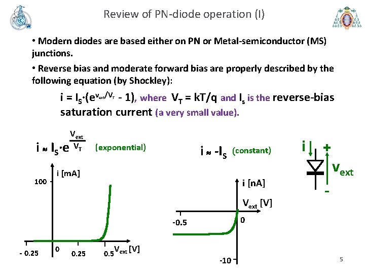
Review of PN-diode operation (I) • Modern diodes are based either on PN or Metal-semiconductor (MS) junctions. • Reverse bias and moderate forward bias are properly described by the following equation (by Shockley): i = IS·(ev /V - 1), where VT = k. T/q and Is is the reverse-bias saturation current (a very small value). ext i » IS 100 Vext ·e VT T i » -IS (exponential) i [m. A] (constant) i [n. A] Vext [V] 0 0. 25 Vext [V] 0. 5 + vext - 0 -0. 5 - 0. 25 i -10 5

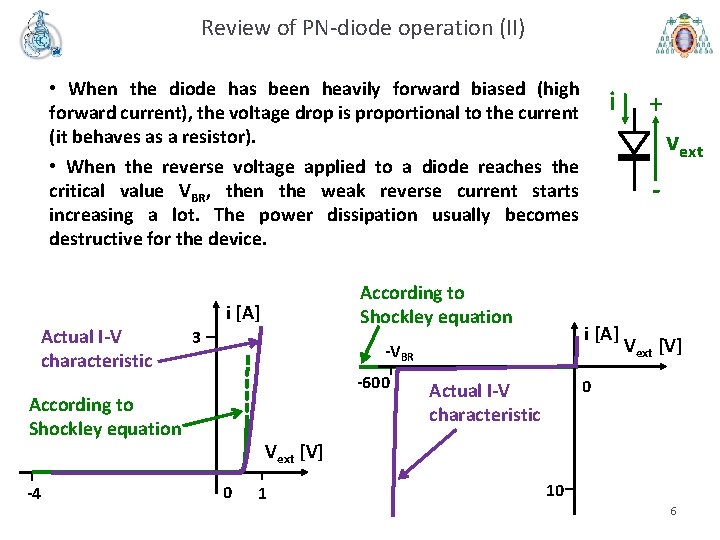
Review of PN-diode operation (II) • When the diode has been heavily forward biased (high forward current), the voltage drop is proportional to the current (it behaves as a resistor). • When the reverse voltage applied to a diode reaches the critical value VBR, then the weak reverse current starts increasing a lot. The power dissipation usually becomes destructive for the device. According to Shockley equation i [A] Actual I-V characteristic 3 According to Shockley equation -4 + vext - i [A] -VBR -600 i Vext [V] 0 Actual I-V characteristic Vext [V] 0 1 10 6

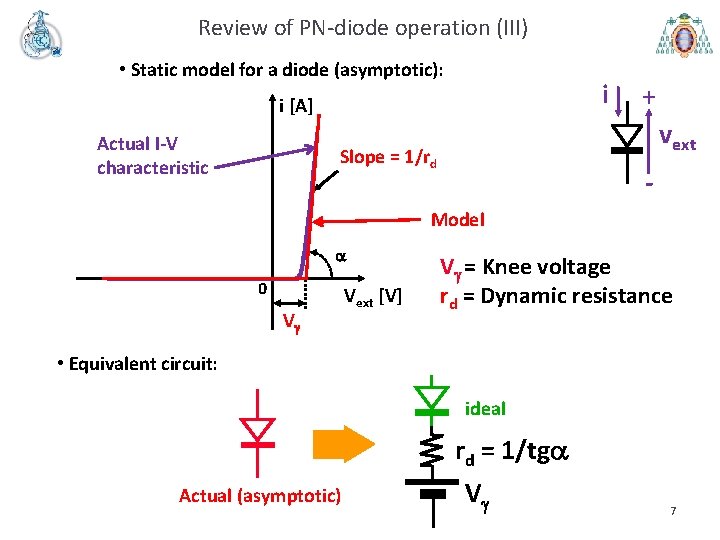
Review of PN-diode operation (III) • Static model for a diode (asymptotic): i i [A] Actual I-V characteristic + vext Slope = 1/rd - Model a 0 V Vext [V] V = Knee voltage rd = Dynamic resistance • Equivalent circuit: ideal rd = 1/tga Actual (asymptotic) V 7
![Review of PNdiode operation IV Ideal diode i i A vext Review of PN-diode operation (IV) • Ideal diode: i + i [A] vext -](https://slidetodoc.com/presentation_image_h/f3646c7654092090bacde84214ac05bf/image-8.jpg)
Review of PN-diode operation (IV) • Ideal diode: i + i [A] vext - Whatever the forward current is, the forward voltage drop is always zero. Ideal diode 0 Whatever the reverse voltage is, the reverse current is always zero. Vext [V] • The ideal diode behaves as a shortcircuit in forward bias. • The ideal diode behaves as a opencircuit in reverse bias. 8

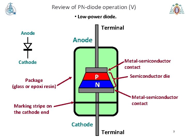
Review of PN-diode operation (V) • Low-power diode. Anode Terminal Anode Metal-semiconductor contact Cathode P N Package (glass or epoxi resin) Semiconductor die Metal-semiconductor contact Marking stripe on the cathode end Cathode Terminal 9

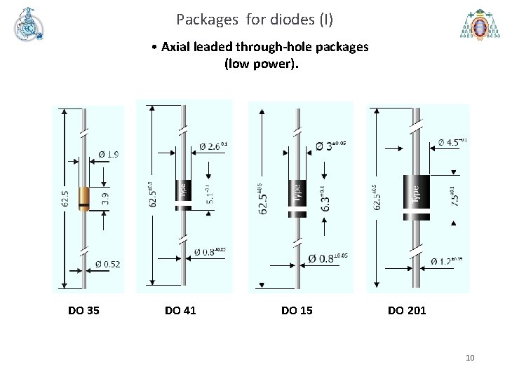
Packages for diodes (I) • Axial leaded through-hole packages (low power). DO 35 DO 41 DO 15 DO 201 10

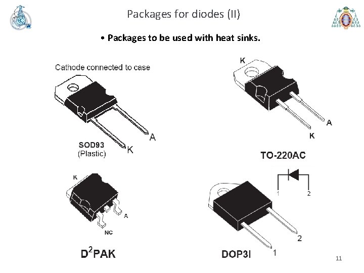
Packages for diodes (II) • Packages to be used with heat sinks. 11

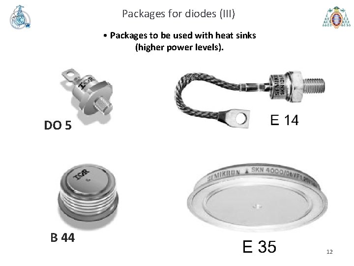
Packages for diodes (III) • Packages to be used with heat sinks (higher power levels). DO 5 B 44 12

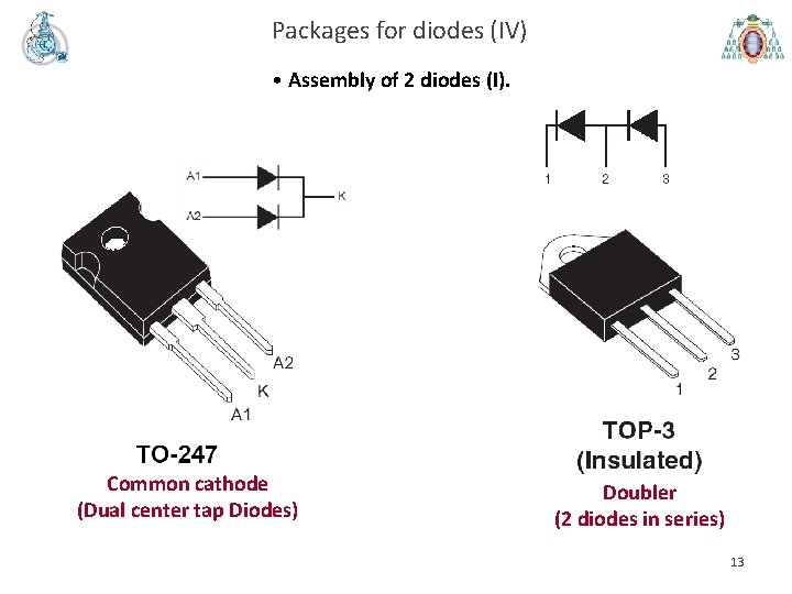
Packages for diodes (IV) • Assembly of 2 diodes (I). Common cathode (Dual center tap Diodes) Doubler (2 diodes in series) 13

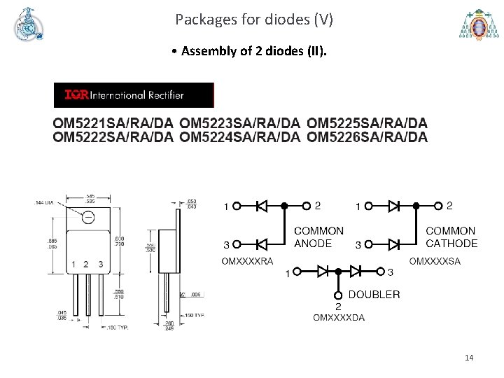
Packages for diodes (V) • Assembly of 2 diodes (II). 14

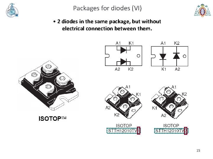
Packages for diodes (VI) • 2 diodes in the same package, but without electrical connection between them. 15

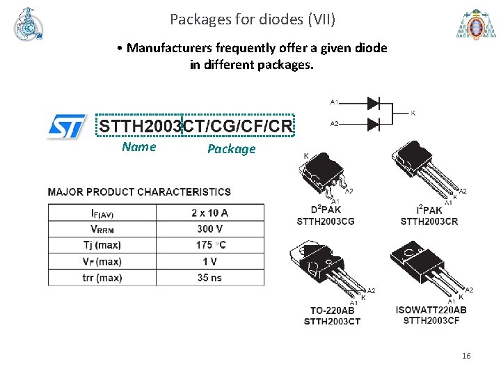
Packages for diodes (VII) • Manufacturers frequently offer a given diode in different packages. Name Package 16

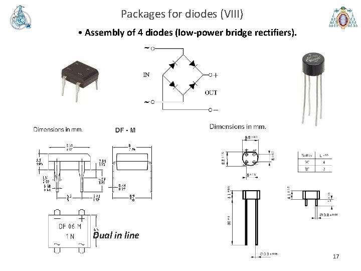
Packages for diodes (VIII) • Assembly of 4 diodes (low-power bridge rectifiers). Dual in line 17

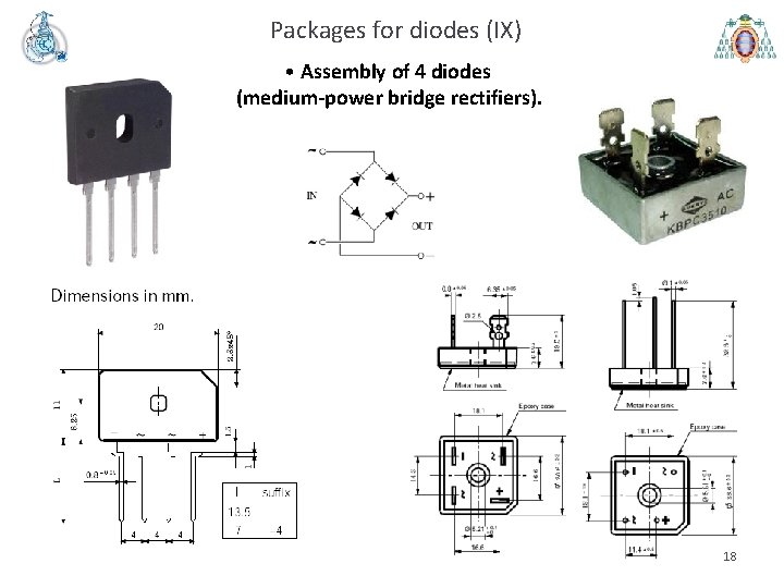
Packages for diodes (IX) • Assembly of 4 diodes (medium-power bridge rectifiers). 18

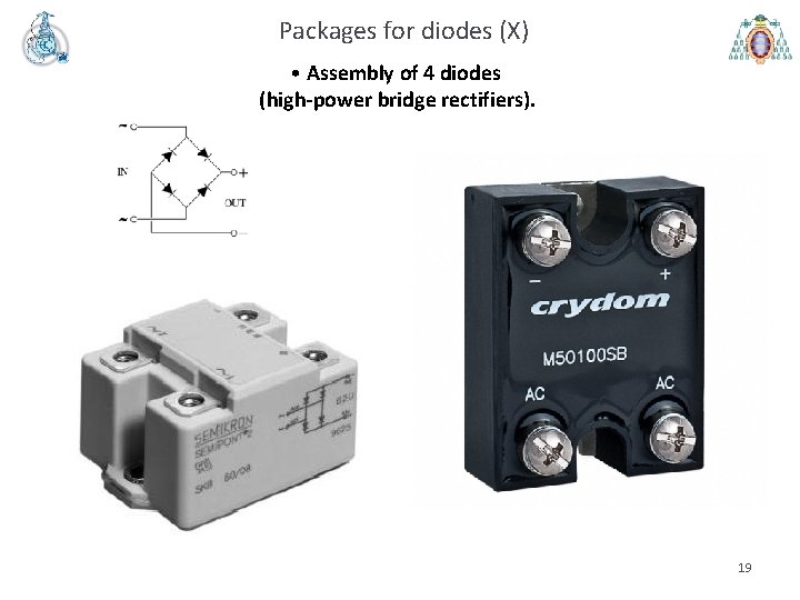
Packages for diodes (X) • Assembly of 4 diodes (high-power bridge rectifiers). 19

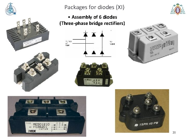
Packages for diodes (XI) • Assembly of 6 diodes (Three-phase bridge rectifiers). 20

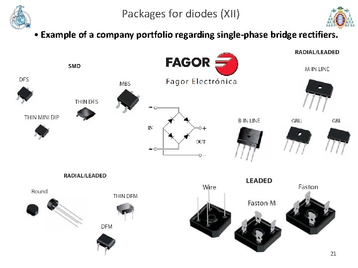
Packages for diodes (XII) • Example of a company portfolio regarding single-phase bridge rectifiers. 21

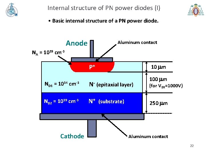
Internal structure of PN power diodes (I) • Basic internal structure of a PN power diode. Anode Aluminum contact NA = 1019 cm-3 P+ ND 1 = 1014 cm-3 ND 2 = 1019 cm-3 Cathode N- 10 mm (epitaxial layer) N+ (substrate) 100 mm (for VBR=1000 V) 250 mm Aluminum contact 22

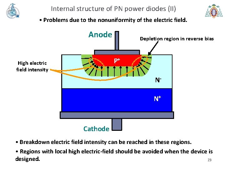
Internal structure of PN power diodes (II) • Problems due to the nonuniformity of the electric field. Anode Depletion region in reverse bias P+ High electric field intensity NN+ Cathode • Breakdown electric field intensity can be reached in these regions. • Regions with local high electric-field should be avoided when the device is designed. 23

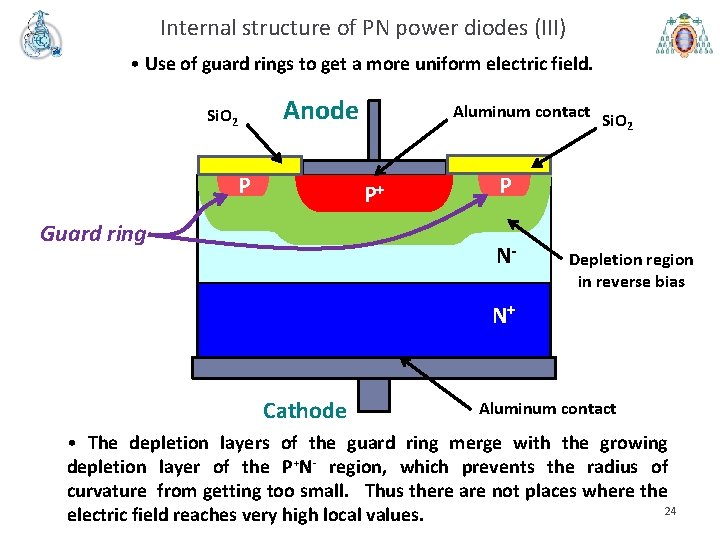
Internal structure of PN power diodes (III) • Use of guard rings to get a more uniform electric field. Si. O 2 Anode P Aluminum contact Si. O 2 P+ Guard ring P N- Depletion region in reverse bias N+ Cathode Aluminum contact • The depletion layers of the guard ring merge with the growing depletion layer of the P+N- region, which prevents the radius of curvature from getting too small. Thus there are not places where the 24 electric field reaches very high local values.

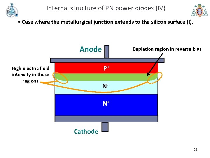
Internal structure of PN power diodes (IV) • Case where the metallurgical junction extends to the silicon surface (I). Anode Depletion region in reverse bias P+ High electric field intensity in these regions NN+ Cathode 25

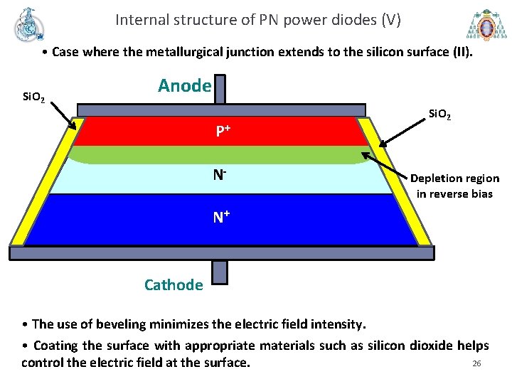
Internal structure of PN power diodes (V) • Case where the metallurgical junction extends to the silicon surface (II). Si. O 2 Anode P+ N- Si. O 2 Depletion region in reverse bias N+ Cathode • The use of beveling minimizes the electric field intensity. • Coating the surface with appropriate materials such as silicon dioxide helps 26 control the electric field at the surface.

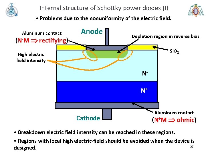
Internal structure of Schottky power diodes (I) • Problems due to the nonuniformity of the electric field. Aluminum contact (N-M Þ rectifying) Anode Depletion region in reverse bias Si. O 2 High electric field intensity NN+ Cathode Aluminum contact (N+M Þ ohmic) • Breakdown electric field intensity can be reached in these regions. • Regions with local high electric-field should be avoided when the device is 27 designed.

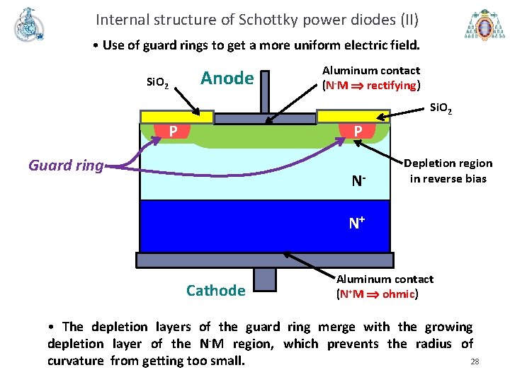
Internal structure of Schottky power diodes (II) • Use of guard rings to get a more uniform electric field. Si. O 2 Anode Aluminum contact (N-M Þ rectifying) Si. O 2 P P Guard ring N- Depletion region in reverse bias N+ Cathode Aluminum contact (N+M Þ ohmic) • The depletion layers of the guard ring merge with the growing depletion layer of the N-M region, which prevents the radius of 28 curvature from getting too small.

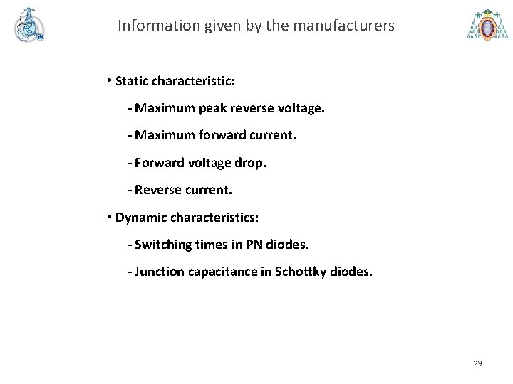
Information given by the manufacturers • Static characteristic: - Maximum peak reverse voltage. - Maximum forward current. - Forward voltage drop. - Reverse current. • Dynamic characteristics: - Switching times in PN diodes. - Junction capacitance in Schottky diodes. 29

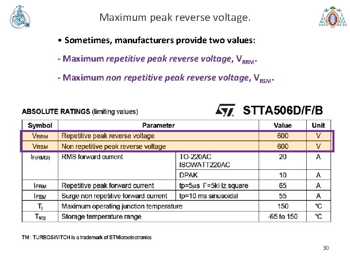
Maximum peak reverse voltage. • Sometimes, manufacturers provide two values: - Maximum repetitive peak reverse voltage, VRRM. - Maximum non repetitive peak reverse voltage, VRSM. 30

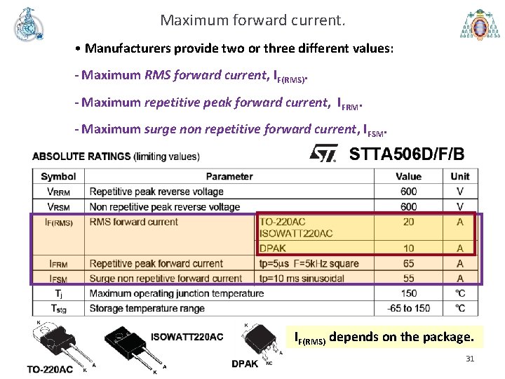
Maximum forward current. • Manufacturers provide two or three different values: - Maximum RMS forward current, IF(RMS). - Maximum repetitive peak forward current, IFRM. - Maximum surge non repetitive forward current, IFSM. IF(RMS) depends on the package. 31

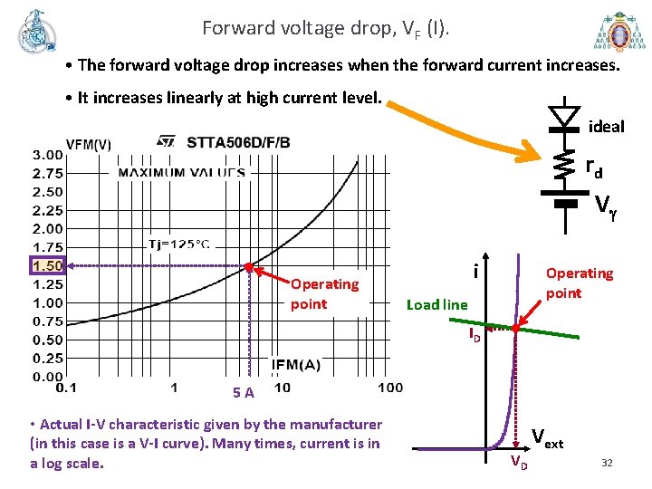
Forward voltage drop, VF (I). • The forward voltage drop increases when the forward current increases. • It increases linearly at high current level. ideal rd V Operating point i Operating point Load line ID 5 A • Actual I-V characteristic given by the manufacturer (in this case is a V-I curve). Many times, current is in a log scale. VD Vext 32

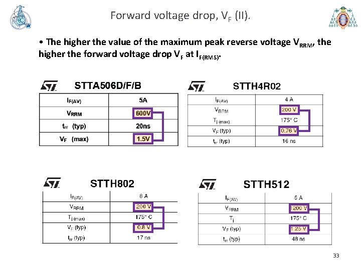
Forward voltage drop, VF (II). • The higher the value of the maximum peak reverse voltage VRRM, the higher the forward voltage drop VF at IF(RMS). 33

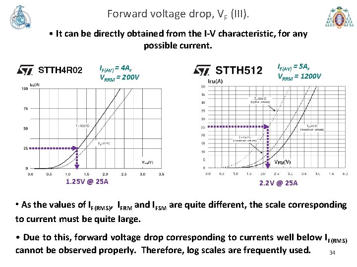
Forward voltage drop, VF (III). • It can be directly obtained from the I-V characteristic, for any possible current. IF(AV) = 4 A, VRRM = 200 V 1. 25 V @ 25 A IF(AV) = 5 A, VRRM = 1200 V 2. 2 V @ 25 A • As the values of IF(RMS), IFRM and IFSM are quite different, the scale corresponding to current must be quite large. • Due to this, forward voltage drop corresponding to currents well below IF(RMS) cannot be observed properly. Therefore, log scales are frequently used. 34

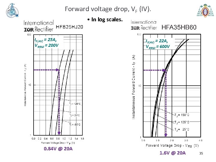
Forward voltage drop, VF (IV). • In log scales. IF(AV) = 25 A, VRRM = 200 V 0. 84 V @ 20 A IF(AV) = 22 A, VRRM = 600 V 1. 6 V @ 20 A 35

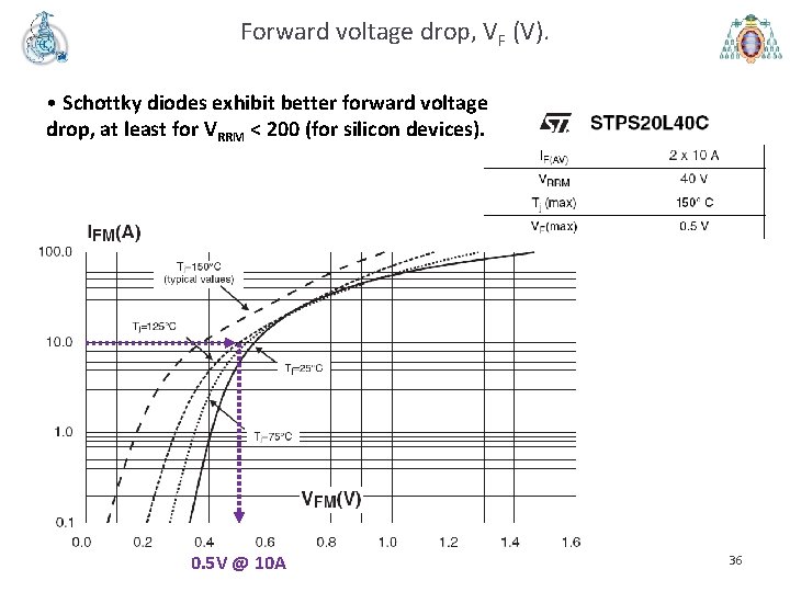
Forward voltage drop, VF (V). • Schottky diodes exhibit better forward voltage drop, at least for VRRM < 200 (for silicon devices). 0. 5 V @ 10 A 36

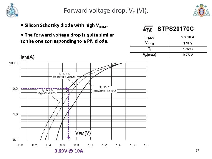
Forward voltage drop, VF (VI). • Silicon Schottky diode with high VRRM. • The forward voltage drop is quite similar to the one corresponding to a PN diode. 0. 69 V @ 10 A 37

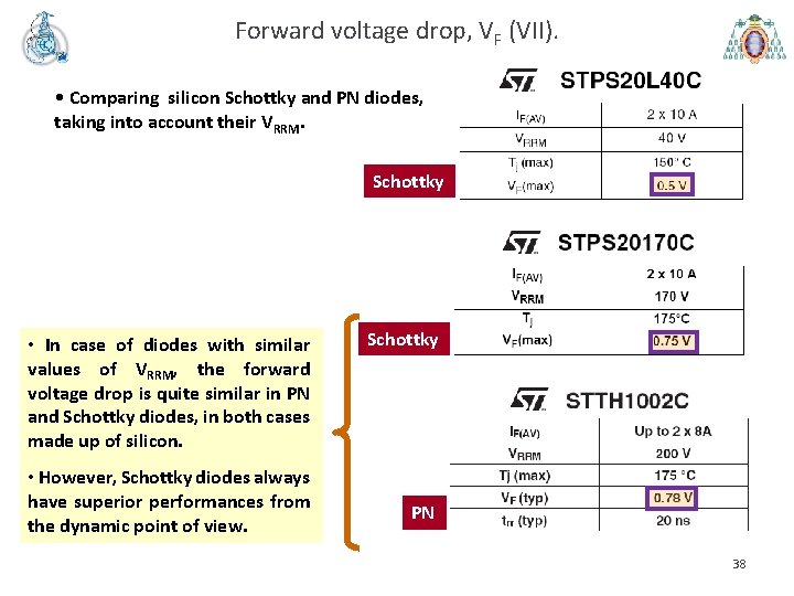
Forward voltage drop, VF (VII). • Comparing silicon Schottky and PN diodes, taking into account their VRRM. Schottky • In case of diodes with similar values of VRRM, the forward voltage drop is quite similar in PN and Schottky diodes, in both cases made up of silicon. • However, Schottky diodes always have superior performances from the dynamic point of view. Schottky PN 38

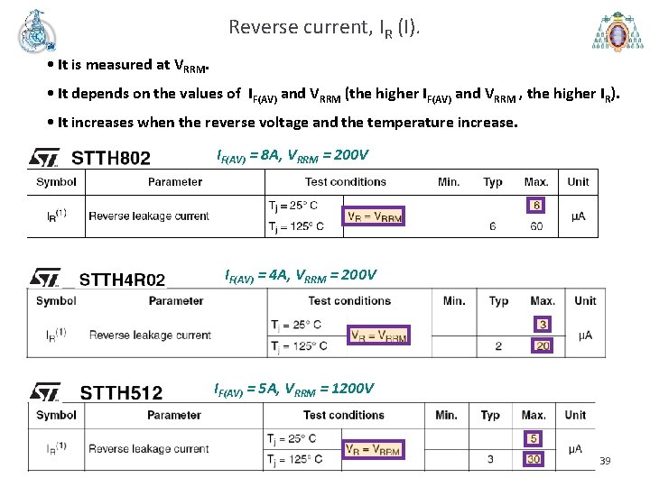
Reverse current, IR (I). • It is measured at VRRM. • It depends on the values of IF(AV) and VRRM (the higher IF(AV) and VRRM , the higher IR). • It increases when the reverse voltage and the temperature increase. IF(AV) = 8 A, VRRM = 200 V IF(AV) = 4 A, VRRM = 200 V IF(AV) = 5 A, VRRM = 1200 V 39

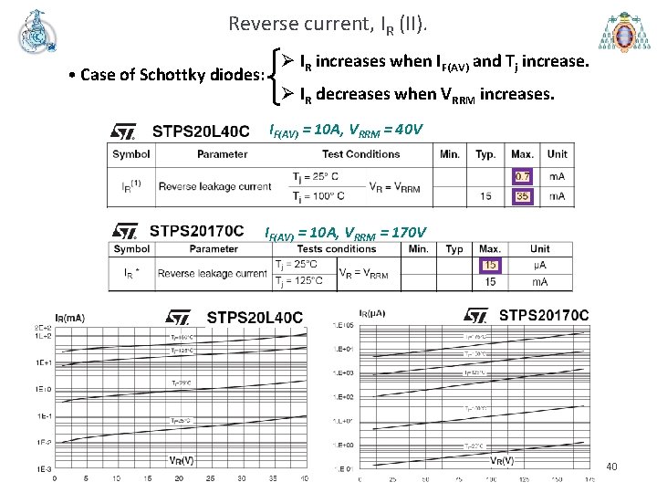
Reverse current, IR (II). • Case of Schottky diodes: Ø IR increases when IF(AV) and Tj increase. Ø IR decreases when VRRM increases. IF(AV) = 10 A, VRRM = 40 V IF(AV) = 10 A, VRRM = 170 V 40

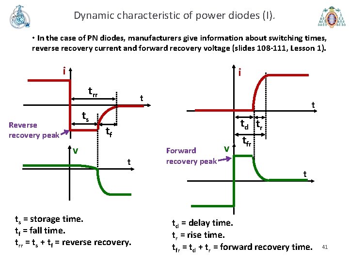
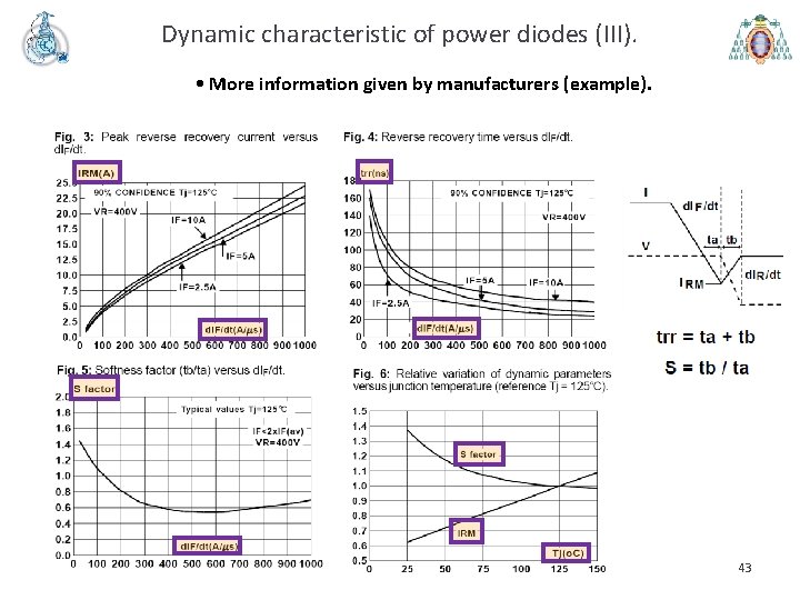
Dynamic characteristic of power diodes (I). • In the case of PN diodes, manufacturers give information about switching times, reverse recovery current and forward recovery voltage (slides 108 -111, Lesson 1). i i trr ts Reverse recovery peak v t t tf t Forward recovery peak v td tr tfr t ts = storage time. tf = fall time. trr = ts + tf = reverse recovery. td = delay time. tr = rise time. tfr = td + tr = forward recovery time. 41

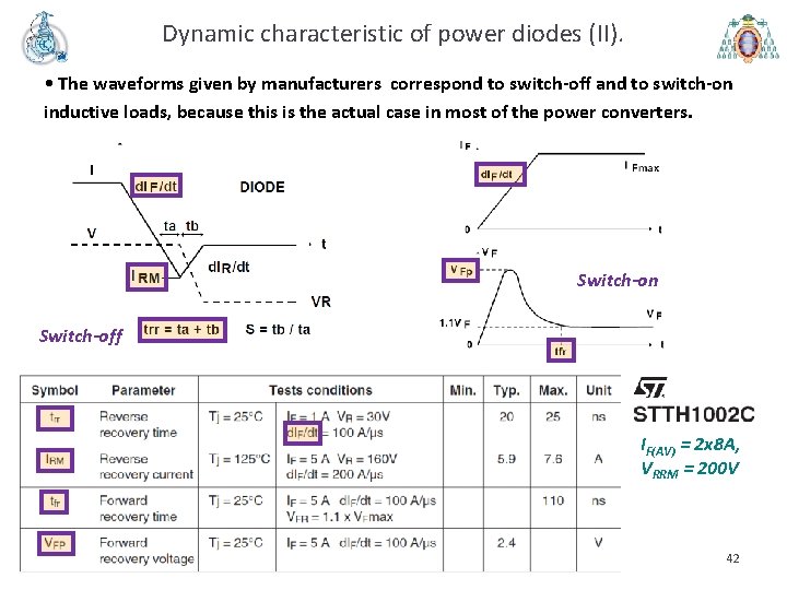
Dynamic characteristic of power diodes (II). • The waveforms given by manufacturers correspond to switch-off and to switch-on inductive loads, because this is the actual case in most of the power converters. Switch-on Switch-off IF(AV) = 2 x 8 A, VRRM = 200 V 42

Dynamic characteristic of power diodes (III). • More information given by manufacturers (example). 43

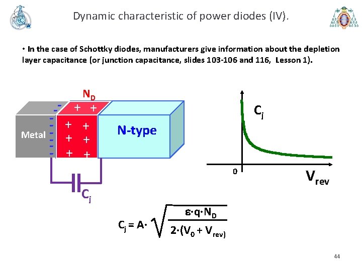
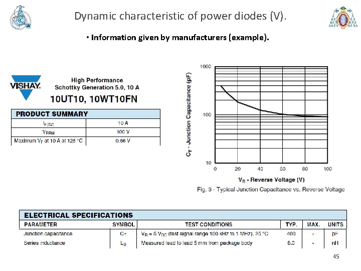
Dynamic characteristic of power diodes (IV). • In the case of Schottky diodes, manufacturers give information about the depletion layer capacitance (or junction capacitance, slides 103 -106 and 116, Lesson 1). ND -- + + Metal -- + + Cj N N-type 0 Cj Cj = A· Vrev ·q·ND 2·(V 0 + Vrev) 44

Dynamic characteristic of power diodes (V). • Information given by manufacturers (example). 45

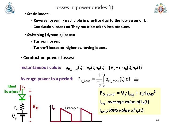
Losses in power diodes (I). • Static losses: - Reverse losses Þ negligible in practice due to the low value of IR. - Conduction losses Þ They must be taken into account. • Switching (dynamic) losses: - Turn-on losses. - Turn-off losses Þ higher switching losses. • Conduction power losses: Instantaneous value: p. D_cond(t) = v. D(t)·i. D(t) = [V + rd·i. D(t)]·i. D(t) Average power in a period: Ideal i. D (lossless) + V PD_cond = V ·Iavg + rd·IRMS 2 v. D rd - Þ i. D Iavg: average value of i. D(t) Example IRMS: RMS value of i. D(t) 46

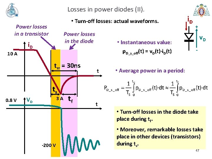
Losses in power diodes (II). • Turn-off losses: actual waveforms. Power losses in a transistor Power losses in the diode i. D • Instantaneous value: p. D_s_off(t) = v. D(t)·i. D(t) 10 A trr = 30 ns ts 0. 8 V 3 A VD tf t i. D + v. D - • Average power in a period: t • Turn-off losses in the diode take place during tf. -200 V • Moreover, remarkable losses take place in other devices (transistors) during ts. 47

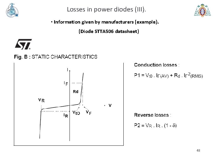
Losses in power diodes (III). • Information given by manufacturers (example). (Diode STTA 506 datasheet) 48

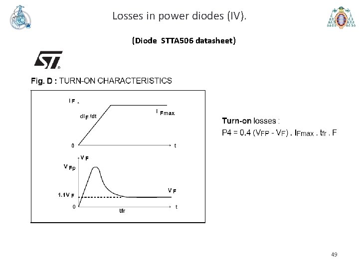
Losses in power diodes (IV). (Diode STTA 506 datasheet) 49

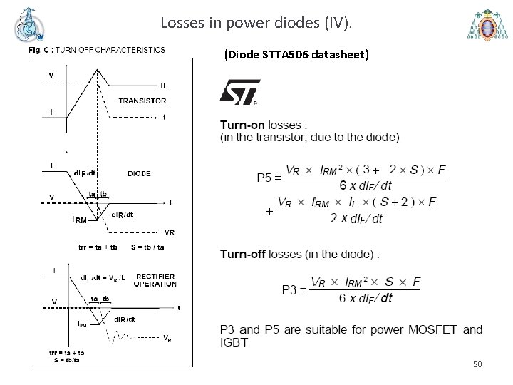
Losses in power diodes (IV). (Diode STTA 506 datasheet) 50