ELEC 7770 Advanced VLSI Design Spring 2014 Timing

- Slides: 38

ELEC 7770 Advanced VLSI Design Spring 2014 Timing Verification and Optimization Vishwani D. Agrawal James J. Danaher Professor ECE Department, Auburn University, Auburn, AL 36849 vagrawal@eng. auburn. edu http: //www. eng. auburn. edu/~vagrawal/COURSE/E 7770_Spr 14/course. html Spring 2014, Feb 5. . . ELEC 7770: Advanced VLSI Design (Agrawal) 1

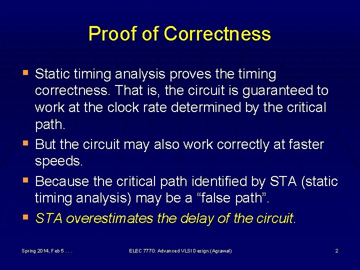
Proof of Correctness § Static timing analysis proves the timing § § § correctness. That is, the circuit is guaranteed to work at the clock rate determined by the critical path. But the circuit may also work correctly at faster speeds. Because the critical path identified by STA (static timing analysis) may be a “false path”. STA overestimates the delay of the circuit. Spring 2014, Feb 5. . . ELEC 7770: Advanced VLSI Design (Agrawal) 2

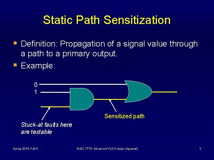
Static Path Sensitization § Definition: Propagation of a signal value through § a path to a primary output. Example: 0 1 Sensitized path Stuck-at faults here are testable Spring 2014, Feb 5. . . ELEC 7770: Advanced VLSI Design (Agrawal) 3

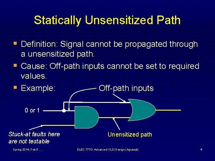
Statically Unsensitized Path § Definition: Signal cannot be propagated through § § a unsensitized path. Cause: Off-path inputs cannot be set to required values. Example: Off-path inputs 0 or 1 Stuck-at faults here are not testable Spring 2014, Feb 5. . . Unensitized path ELEC 7770: Advanced VLSI Design (Agrawal) 4

Dynamically Sensitized Path § Definition: A dynamic signal can be propagated § through a statically unsensitizable path. Example: See later. Spring 2014, Feb 5. . . ELEC 7770: Advanced VLSI Design (Agrawal) 5

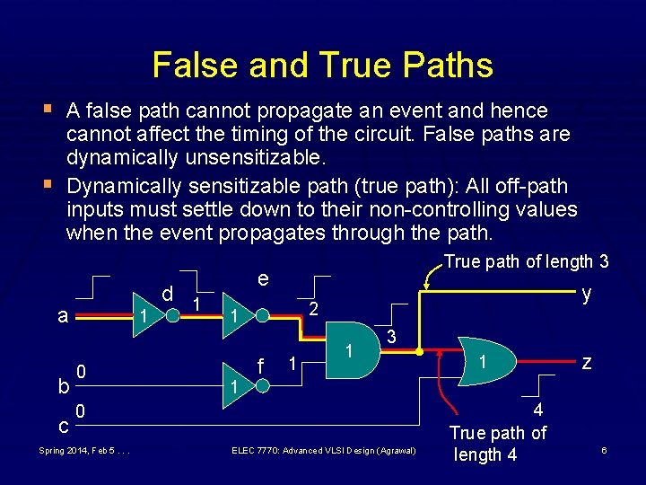
False and True Paths § A false path cannot propagate an event and hence § cannot affect the timing of the circuit. False paths are dynamically unsensitizable. Dynamically sensitizable path (true path): All off-path inputs must settle down to their non-controlling values when the event propagates through the path. a b c 1 0 d 1 True path of length 3 e 2 1 1 y f 1 1 3 0 Spring 2014, Feb 5. . . ELEC 7770: Advanced VLSI Design (Agrawal) 1 4 True path of length 4 z 6

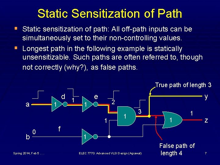
Static Sensitization of Path § Static sensitization of path: All off-path inputs can be § simultaneously set to their non-controlling values. Longest path in the following example is statically unsensitizable. Such paths are often referred to, though not correctly (why? ), as false paths. True path of length 3 a d 1 1 e 2 1 1 b 0 Spring 2014, Feb 5. . . y 1 3 1 1 z f 1 ELEC 7770: Advanced VLSI Design (Agrawal) False path of length 4 7

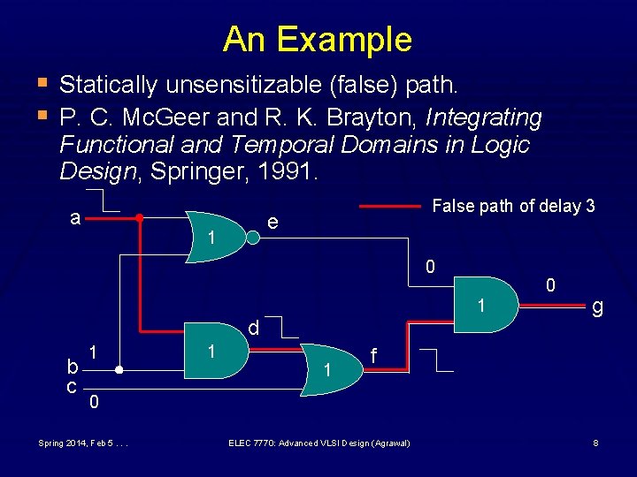
An Example § Statically unsensitizable (false) path. § P. C. Mc. Geer and R. K. Brayton, Integrating Functional and Temporal Domains in Logic Design, Springer, 1991. a False path of delay 3 e 1 0 0 1 d b c 1 1 1 g f 0 Spring 2014, Feb 5. . . ELEC 7770: Advanced VLSI Design (Agrawal) 8

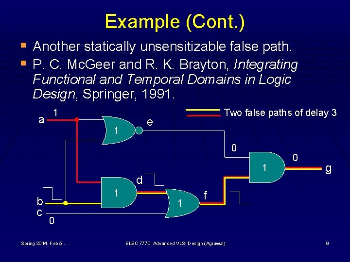
Example (Cont. ) § Another statically unsensitizable false path. § P. C. Mc. Geer and R. K. Brayton, Integrating Functional and Temporal Domains in Logic Design, Springer, 1991. a 1 Two false paths of delay 3 e 1 0 1 d b c 1 1 0 g f 0 Spring 2014, Feb 5. . . ELEC 7770: Advanced VLSI Design (Agrawal) 9

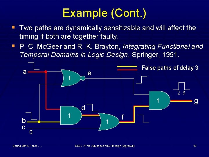
Example (Cont. ) § Two paths are dynamically sensitizable and will affect the § timing if both are together faulty. P. C. Mc. Geer and R. K. Brayton, Integrating Functional and Temporal Domains in Logic Design, Springer, 1991. a False paths of delay 3 e 1 2 3 1 d b c 1 1 g f 0 Spring 2014, Feb 5. . . ELEC 7770: Advanced VLSI Design (Agrawal) 10

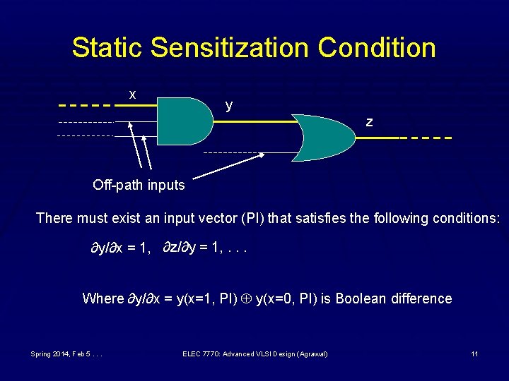
Static Sensitization Condition x y z Off-path inputs There must exist an input vector (PI) that satisfies the following conditions: ∂y/∂x = 1, ∂z/∂y = 1, . . . Where ∂y/∂x = y(x=1, PI) y(x=0, PI) is Boolean difference Spring 2014, Feb 5. . . ELEC 7770: Advanced VLSI Design (Agrawal) 11

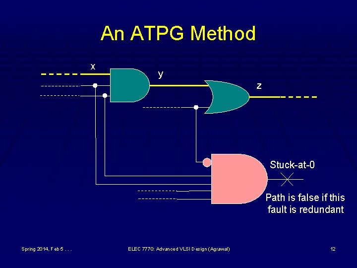
An ATPG Method x y z Stuck-at-0 Path is false if this fault is redundant Spring 2014, Feb 5. . . ELEC 7770: Advanced VLSI Design (Agrawal) 12

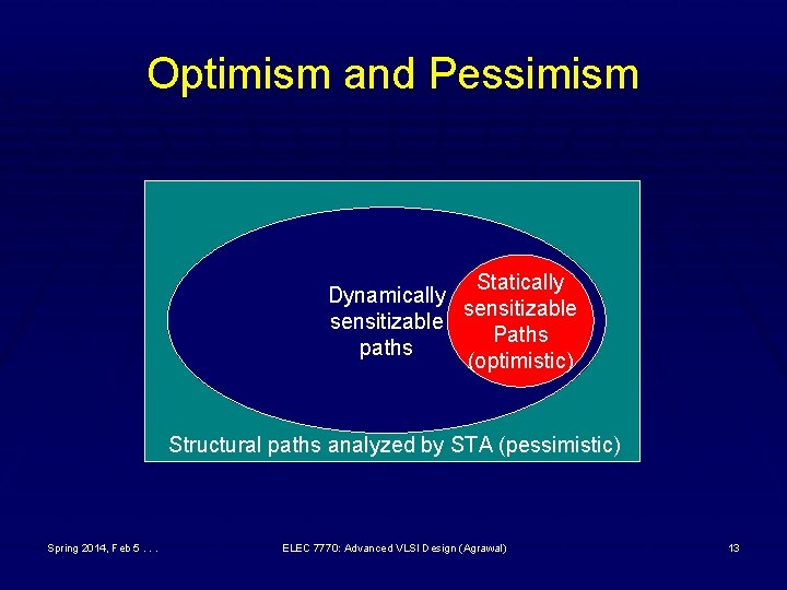
Optimism and Pessimism Statically Dynamically sensitizable Paths paths (optimistic) Structural paths analyzed by STA (pessimistic) Spring 2014, Feb 5. . . ELEC 7770: Advanced VLSI Design (Agrawal) 13

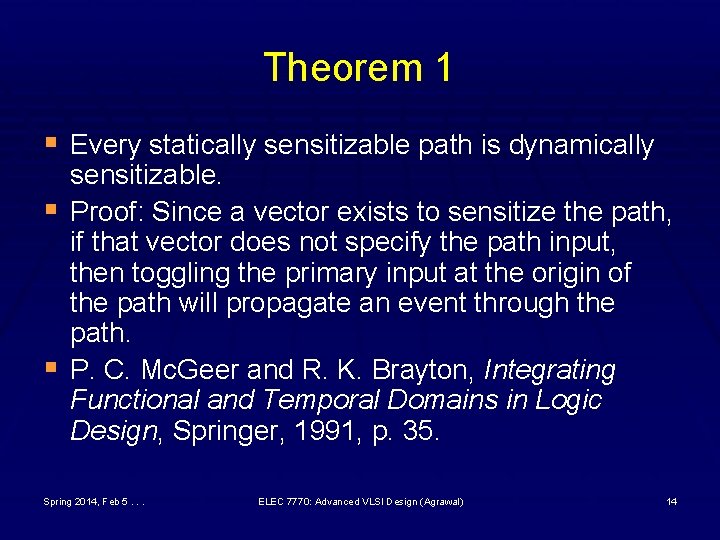
Theorem 1 § Every statically sensitizable path is dynamically § § sensitizable. Proof: Since a vector exists to sensitize the path, if that vector does not specify the path input, then toggling the primary input at the origin of the path will propagate an event through the path. P. C. Mc. Geer and R. K. Brayton, Integrating Functional and Temporal Domains in Logic Design, Springer, 1991, p. 35. Spring 2014, Feb 5. . . ELEC 7770: Advanced VLSI Design (Agrawal) 14

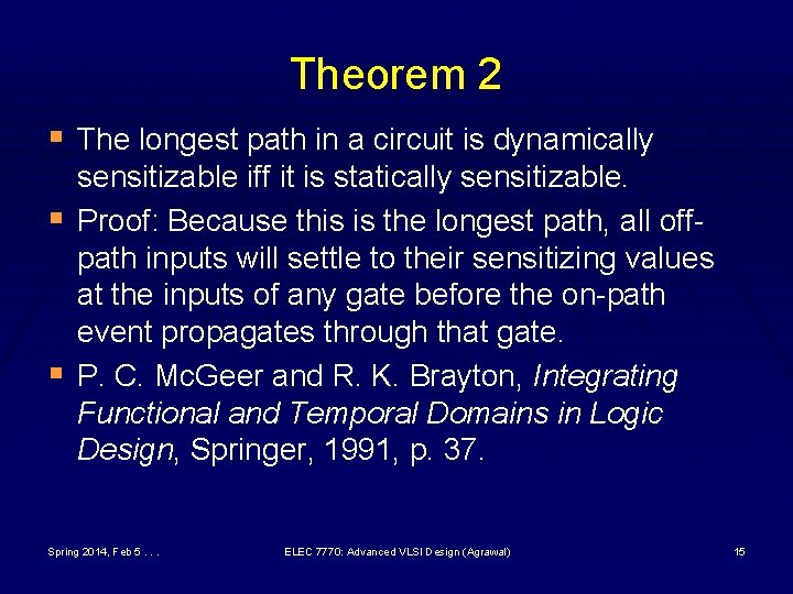
Theorem 2 § The longest path in a circuit is dynamically § § sensitizable iff it is statically sensitizable. Proof: Because this is the longest path, all offpath inputs will settle to their sensitizing values at the inputs of any gate before the on-path event propagates through that gate. P. C. Mc. Geer and R. K. Brayton, Integrating Functional and Temporal Domains in Logic Design, Springer, 1991, p. 37. Spring 2014, Feb 5. . . ELEC 7770: Advanced VLSI Design (Agrawal) 15

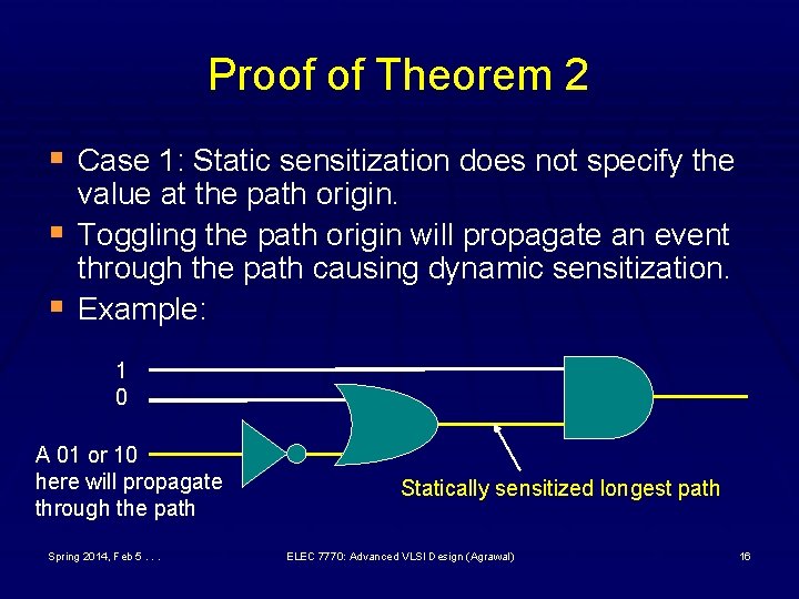
Proof of Theorem 2 § Case 1: Static sensitization does not specify the § § value at the path origin. Toggling the path origin will propagate an event through the path causing dynamic sensitization. Example: 1 0 A 01 or 10 here will propagate through the path Spring 2014, Feb 5. . . Statically sensitized longest path ELEC 7770: Advanced VLSI Design (Agrawal) 16

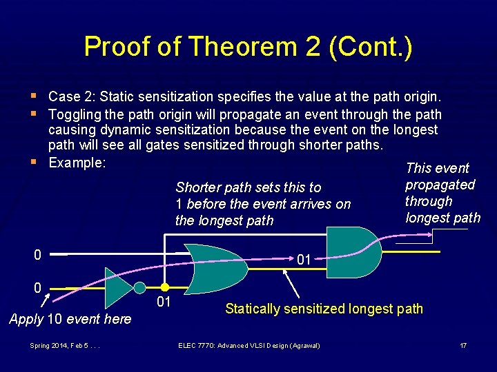
Proof of Theorem 2 (Cont. ) § Case 2: Static sensitization specifies the value at the path origin. § Toggling the path origin will propagate an event through the path § causing dynamic sensitization because the event on the longest path will see all gates sensitized through shorter paths. Example: This event Shorter path sets this to 1 before the event arrives on the longest path 0 0 Apply 10 event here Spring 2014, Feb 5. . . propagated through longest path 01 01 Statically sensitized longest path ELEC 7770: Advanced VLSI Design (Agrawal) 17

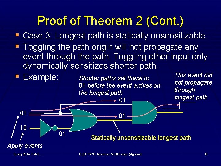
Proof of Theorem 2 (Cont. ) § Case 3: Longest path is statically unsensitizable. § Toggling the path origin will not propagate any § event through the path. Toggling other input only dynamically sensitizes shorter path. This event did Example: Shorter paths set these to 01 before the event arrives on the longest path 01 01 10 not propagate through longest path 01 01 Statically unsensitizable longest path Apply events Spring 2014, Feb 5. . . ELEC 7770: Advanced VLSI Design (Agrawal) 18

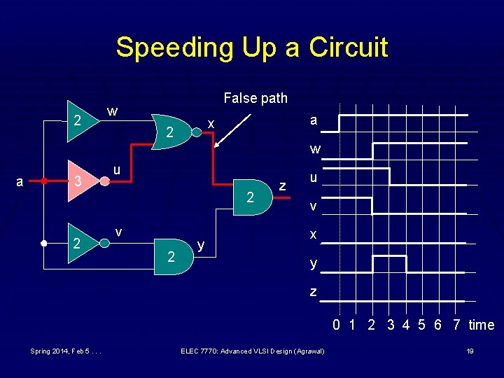
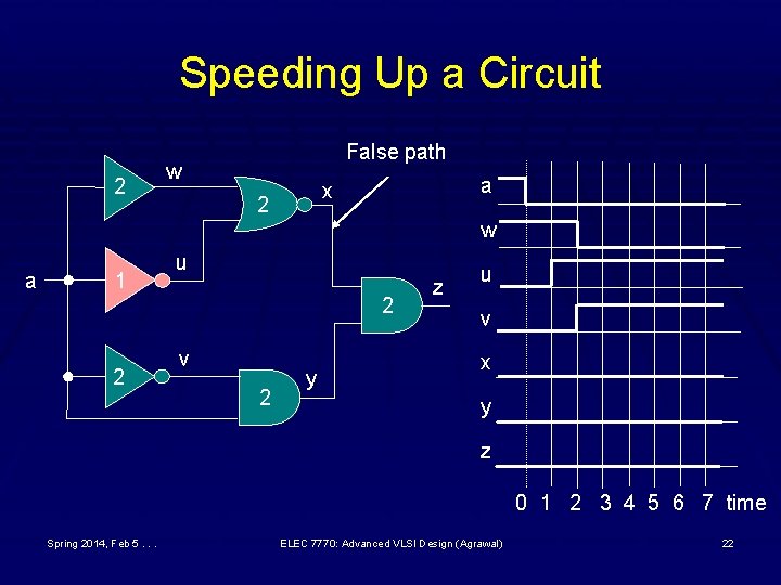
Speeding Up a Circuit 2 False path w a x 2 w a 3 u 2 2 v 2 y z u v x y z 0 1 2 3 4 5 6 7 time Spring 2014, Feb 5. . . ELEC 7770: Advanced VLSI Design (Agrawal) 19

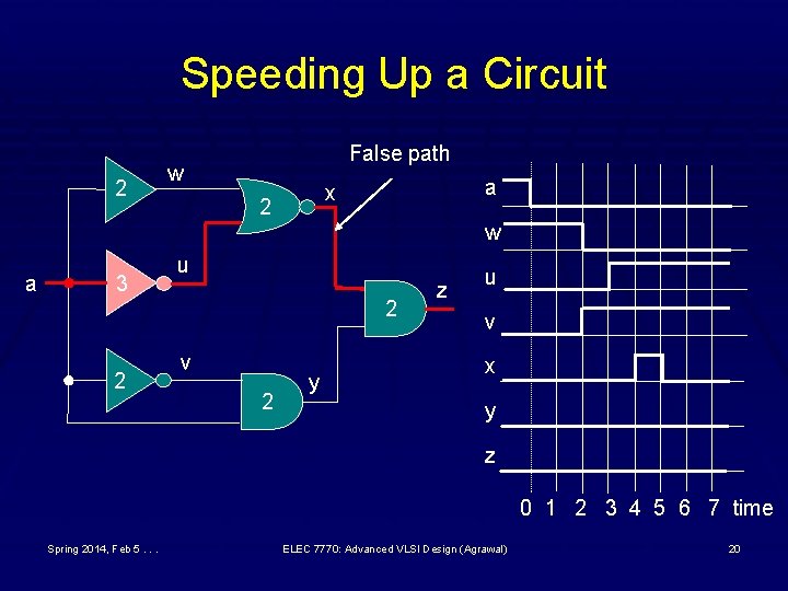
Speeding Up a Circuit 2 False path w a x 2 w a 3 u 2 2 v 2 y z u v x y z 0 1 2 3 4 5 6 7 time Spring 2014, Feb 5. . . ELEC 7770: Advanced VLSI Design (Agrawal) 20

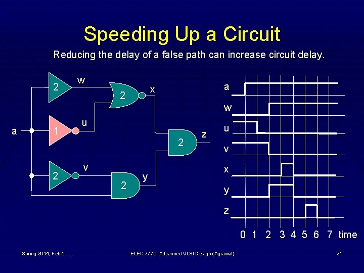
Speeding Up a Circuit Reducing the delay of a false path can increase circuit delay. 2 w a x 2 w a 1 u 2 2 v 2 y z u v x y z 0 1 2 3 4 5 6 7 time Spring 2014, Feb 5. . . ELEC 7770: Advanced VLSI Design (Agrawal) 21

Speeding Up a Circuit 2 False path w a x 2 w a 1 u 2 2 v 2 y z u v x y z 0 1 2 3 4 5 6 7 time Spring 2014, Feb 5. . . ELEC 7770: Advanced VLSI Design (Agrawal) 22

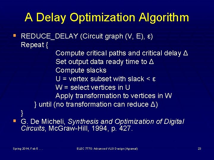
A Delay Optimization Algorithm § REDUCE_DELAY (Circuit graph (V, E), ε) Repeat { Compute critical paths and critical delay Δ Set output data ready time to Δ Compute slacks U = vertex subset with slack < ε W = select vertices in U Apply transformation to vertices in W } until (no transformation can reduce Δ) § } G. De Micheli, Synthesis and Optimization of Digital Circuits, Mc. Graw-Hill, 1994, p. 427. Spring 2014, Feb 5. . . ELEC 7770: Advanced VLSI Design (Agrawal) 23

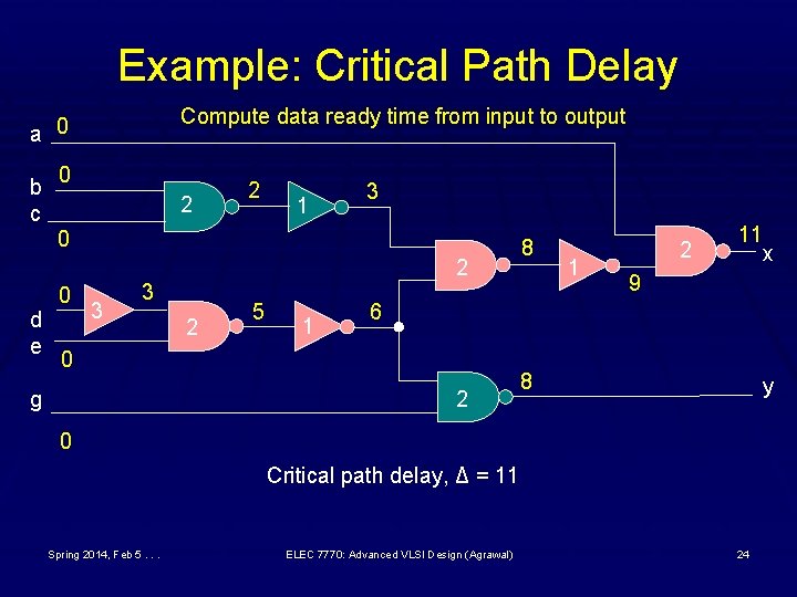
Example: Critical Path Delay Compute data ready time from input to output a 0 b c 0 2 2 1 3 0 d e 0 3 2 5 1 1 2 11 x 9 6 0 g 8 2 8 y 0 Critical path delay, Δ = 11 Spring 2014, Feb 5. . . ELEC 7770: Advanced VLSI Design (Agrawal) 24

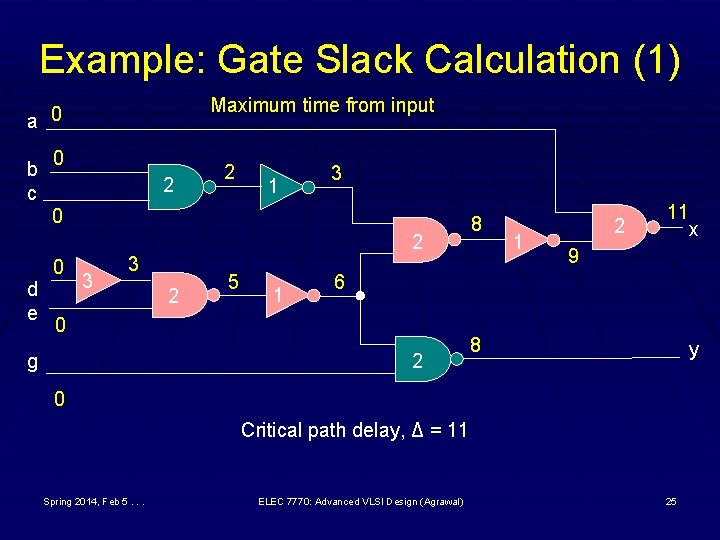
Example: Gate Slack Calculation (1) Maximum time from input a 0 b c 0 2 2 1 3 0 d e 0 3 2 5 1 1 2 11 x 9 6 0 g 8 2 8 y 0 Critical path delay, Δ = 11 Spring 2014, Feb 5. . . ELEC 7770: Advanced VLSI Design (Agrawal) 25

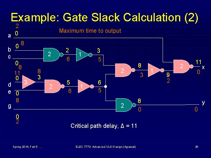
Example: Gate Slack Calculation (2) 2 a 0 b c Maximum time to output 08 2 0 8 11 0 3 d e 0 8 g Spring 2014, Feb 5. . . 1 3 5 2 8 3 0 2 2 6 2 5 6 1 8 3 6 5 2 8 0 1 2 9 2 11 x 0 y 0 Critical path delay, Δ = 11 ELEC 7770: Advanced VLSI Design (Agrawal) 26

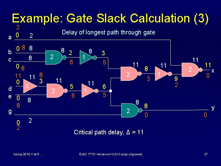
Example: Gate Slack Calculation (3) 2 a 0 b c Delay of longest path through gate 2 08 8 8 08 11 11 8 3 0 3 d e 0 8 8 g 0 2 2 8 2 6 11 2 1 8 3 5 11 2 5 6 11 1 3 6 5 8 2 2 Spring 2014, Feb 5. . . 8 8 0 11 1 11 2 9 2 11 x 0 y 0 Critical path delay, Δ = 11 ELEC 7770: Advanced VLSI Design (Agrawal) 27

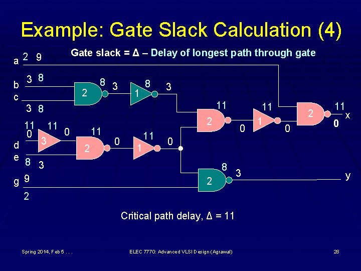
Example: Gate Slack Calculation (4) Gate slack = Δ – Delay of longest path through gate a 2 9 b c 3 8 2 8 3 11 3 8 d e 11 0 11 3 11 0 8 3 g 9 2 2 0 11 1 2 0 11 x 0 0 8 2 3 y 2 Critical path delay, Δ = 11 Spring 2014, Feb 5. . . ELEC 7770: Advanced VLSI Design (Agrawal) 28

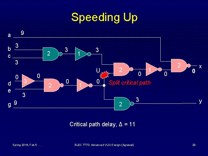
Speeding Up 9 a b c 3 2 3 1 3 3 d e 0 3 U 0 2 0 1 0 2 0 Split critical path 3 g 9 1 2 2 0 0 3 y Critical path delay, Δ = 11 Spring 2014, Feb 5. . . ELEC 7770: Advanced VLSI Design (Agrawal) x 29

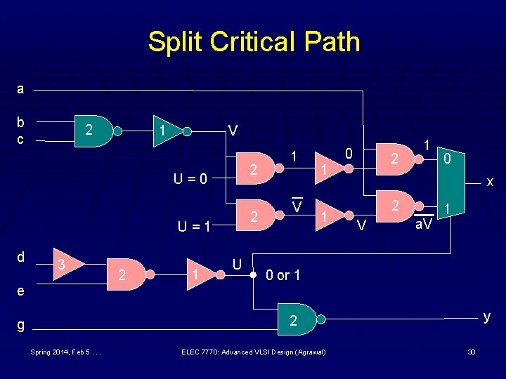
Split Critical Path a b c 2 V 1 2 U=0 2 U=1 d 3 e 2 1 U 1 V 0 2 1 1 1 0 x 2 V a. V 1 0 or 1 y 2 g Spring 2014, Feb 5. . . ELEC 7770: Advanced VLSI Design (Agrawal) 30

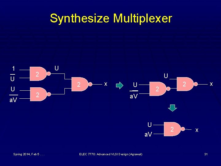
Synthesize Multiplexer 1 U U a. V 2 U U 2 2 x U 2 a. V U a. V Spring 2014, Feb 5. . . x 2 ELEC 7770: Advanced VLSI Design (Agrawal) 2 x 31

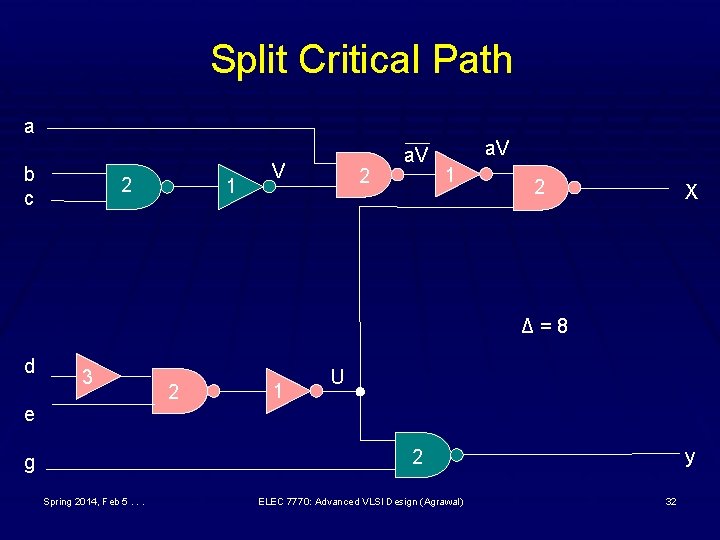
Split Critical Path a b c 2 1 V 2 a. V 1 2 X Δ=8 d 3 e 2 1 U y 2 g Spring 2014, Feb 5. . . ELEC 7770: Advanced VLSI Design (Agrawal) 32

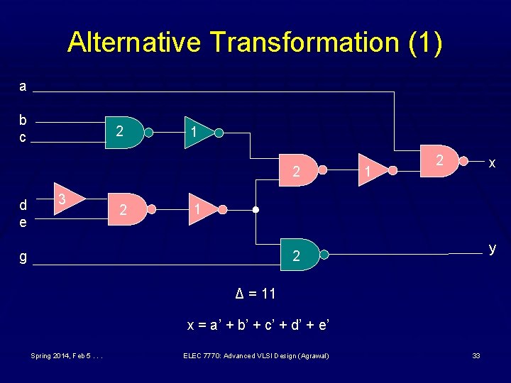
Alternative Transformation (1) a b c 2 1 2 d e 3 2 1 2 x 1 g y 2 Δ = 11 x = a’ + b’ + c’ + d’ + e’ Spring 2014, Feb 5. . . ELEC 7770: Advanced VLSI Design (Agrawal) 33

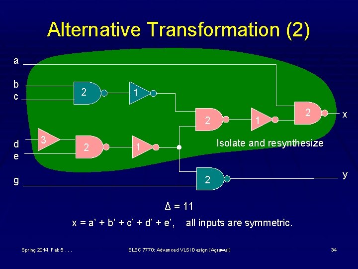
Alternative Transformation (2) a b c 2 1 2 d e 3 2 1 2 x Isolate and resynthesize 1 g y 2 Δ = 11 x = a’ + b’ + c’ + d’ + e’, Spring 2014, Feb 5. . . all inputs are symmetric. ELEC 7770: Advanced VLSI Design (Agrawal) 34

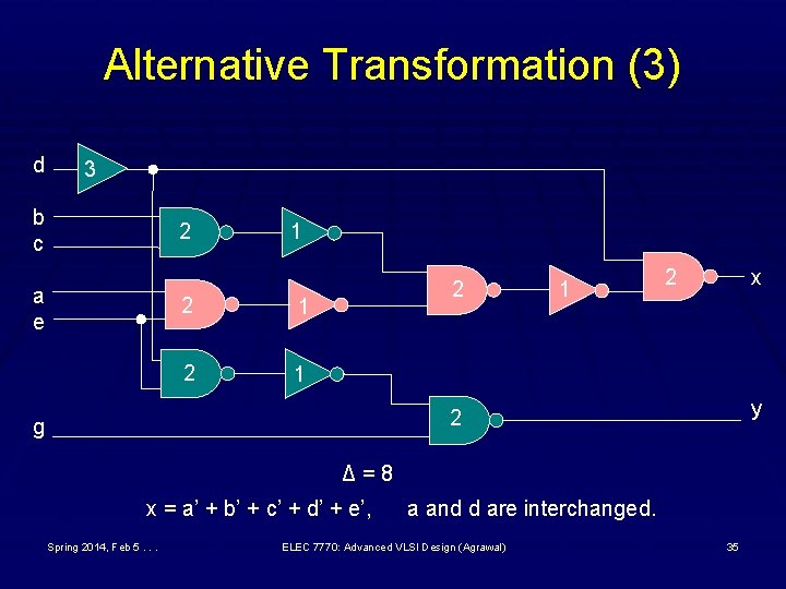
Alternative Transformation (3) d 3 b c 2 a e 1 2 1 2 x y 2 g Δ=8 x = a’ + b’ + c’ + d’ + e’, Spring 2014, Feb 5. . . a and d are interchanged. ELEC 7770: Advanced VLSI Design (Agrawal) 35

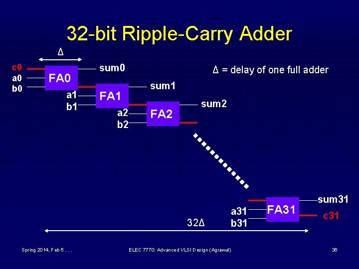
32 -bit Ripple-Carry Adder Δ c 0 a 0 b 0 FA 0 a 1 b 1 sum 0 FA 1 a 2 b 2 Δ = delay of one full adder sum 1 FA 2 sum 2 32Δ Spring 2014, Feb 5. . . a 31 b 31 ELEC 7770: Advanced VLSI Design (Agrawal) FA 31 sum 31 c 31 36

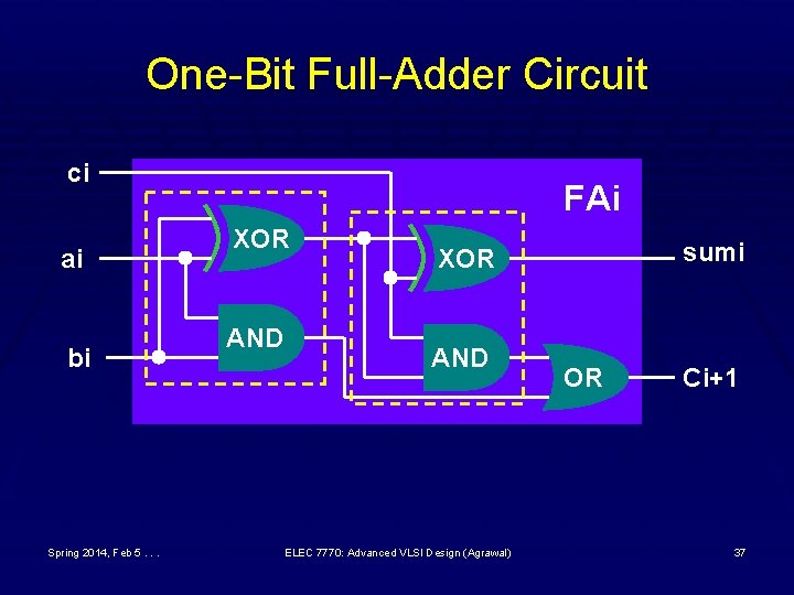
One-Bit Full-Adder Circuit ci ai bi Spring 2014, Feb 5. . . FAi XOR AND sumi XOR AND ELEC 7770: Advanced VLSI Design (Agrawal) OR Ci+1 37

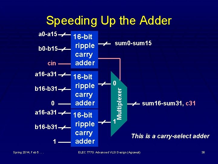
Speeding Up the Adder b 0 -b 15 cin a 16 -a 31 b 16 -b 31 0 a 16 -a 31 b 16 -b 31 1 Spring 2014, Feb 5. . . 16 -bit ripple carry adder sum 0 -sum 15 0 Multiplexer a 0 -a 15 sum 16 -sum 31, c 31 1 This is a carry-select adder ELEC 7770: Advanced VLSI Design (Agrawal) 38