ELEC 7770 Advanced VLSI Design Spring 2012 A


- Slides: 23

ELEC 7770 Advanced VLSI Design Spring 2012 A Linear Programming Solution to Clock Constraint Problem Vishwani D. Agrawal James J. Danaher Professor ECE Department, Auburn University, Auburn, AL 36849 vagrawal@eng. auburn. edu http: //www. eng. auburn. edu/~vagrawal/COURSE/E 7770_Spr 12/course. html Spring 2012, Feb 27. . . ELEC 7770: Advanced VLSI Design (Agrawal) 1

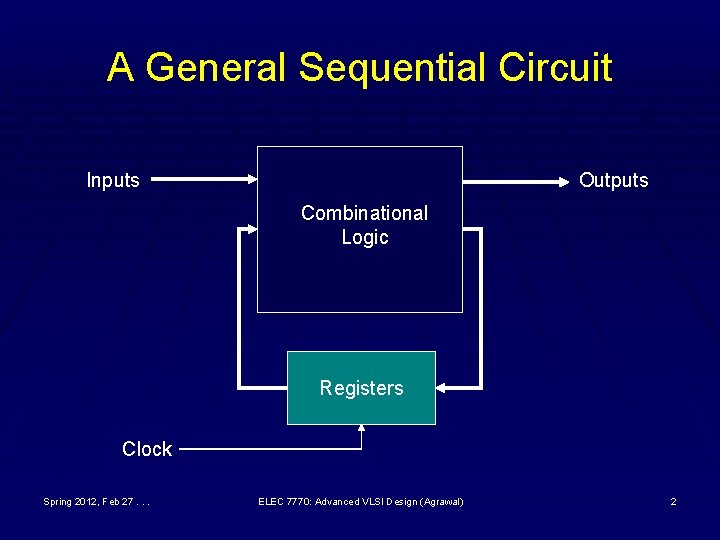
A General Sequential Circuit Inputs Outputs Combinational Logic Registers Clock Spring 2012, Feb 27. . . ELEC 7770: Advanced VLSI Design (Agrawal) 2

A Level-Sensitive Latch D QN Q CK Clock period, Tck CK Latch open Spring 2012, Feb 27. . . Latch closed ELEC 7770: Advanced VLSI Design (Agrawal) Latch open time 3

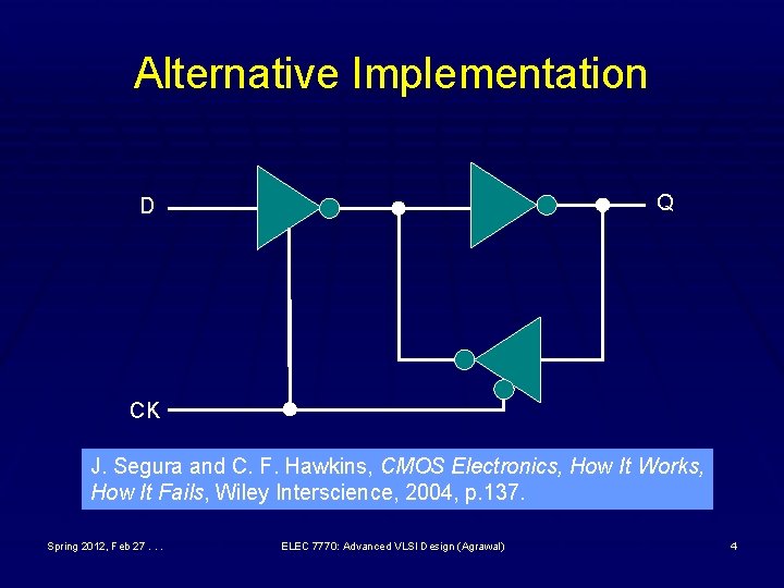
Alternative Implementation Q D CK J. Segura and C. F. Hawkins, CMOS Electronics, How It Works, How It Fails, Wiley Interscience, 2004, p. 137. Spring 2012, Feb 27. . . ELEC 7770: Advanced VLSI Design (Agrawal) 4

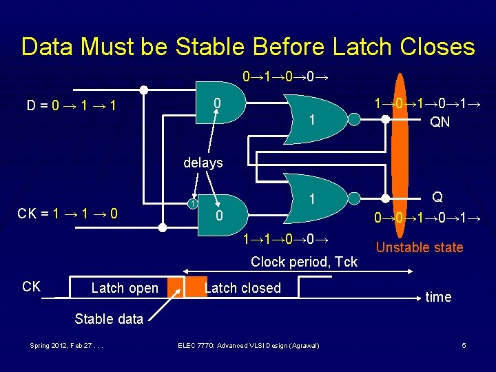
Data Must be Stable Before Latch Closes 0→ 1→ 0→ 0→ 0 D=0→ 1→ 1 1 1→ 0→ 1→ QN delays CK = 1 → 0 1 1 0 0→ 0→ 1→ 1→ 1→ 0→ 0→ Clock period, Tck CK Latch open Q Latch closed Unstable state time Stable data Spring 2012, Feb 27. . . ELEC 7770: Advanced VLSI Design (Agrawal) 5

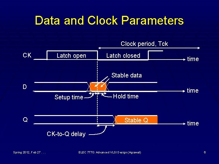
Data and Clock Parameters Clock period, Tck CK Latch open Latch closed time Stable data D Setup time Q Hold time Stable Q time CK-to-Q delay Spring 2012, Feb 27. . . ELEC 7770: Advanced VLSI Design (Agrawal) 6

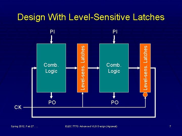
Design With Level-Sensitive Latches CK Spring 2012, Feb 27. . . PO Comb. Logic Level-sens. Latches Comb. Logic PI Level-sens. Latches PI PO ELEC 7770: Advanced VLSI Design (Agrawal) 7

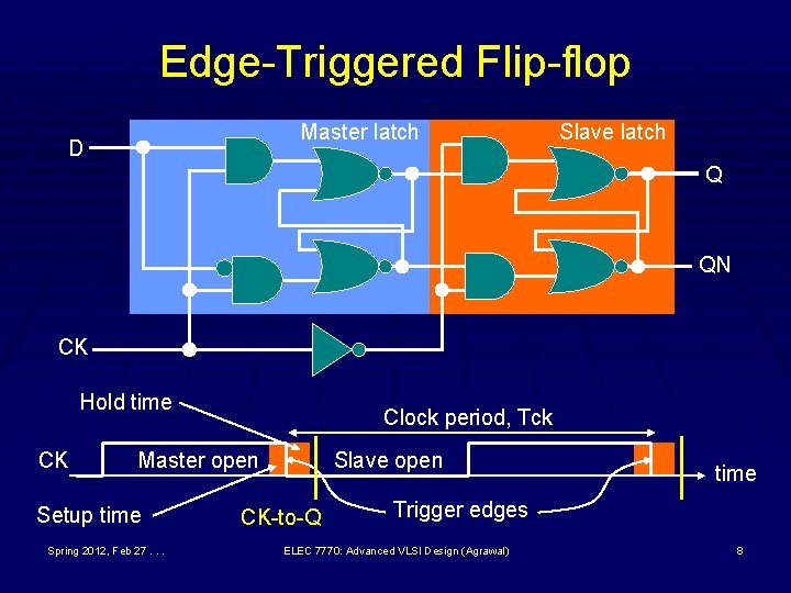
Edge-Triggered Flip-flop Master latch D Slave latch Q QN CK Hold time CK Clock period, Tck Master open Setup time Spring 2012, Feb 27. . . Slave open CK-to-Q time Trigger edges ELEC 7770: Advanced VLSI Design (Agrawal) 8

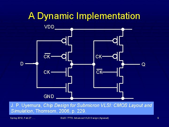
A Dynamic Implementation VDD CK CK D Q CK CK GND J. P. Uyemura, Chip Design for Submicron VLSI: CMOS Layout and Simulation, Thomsom, 2006, p. 229. Spring 2012, Feb 27. . . ELEC 7770: Advanced VLSI Design (Agrawal) 9

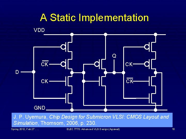
A Static Implementation VDD Q CK CK D GND J. P. Uyemura, Chip Design for Submicron VLSI: CMOS Layout and Simulation, Thomsom, 2006, p. 230. Spring 2012, Feb 27. . . ELEC 7770: Advanced VLSI Design (Agrawal) 10

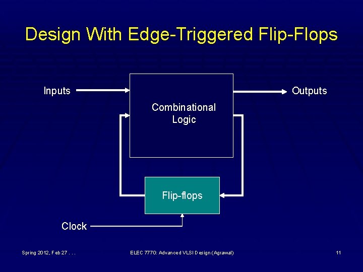
Design With Edge-Triggered Flip-Flops Inputs Outputs Combinational Logic Flip-flops Clock Spring 2012, Feb 27. . . ELEC 7770: Advanced VLSI Design (Agrawal) 11

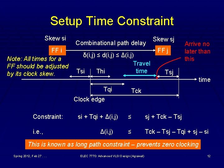
Setup Time Constraint Skew si FF i Note: All times for a FF should be adjusted by its clock skew. Combinational path delay δ(i, j) ≤ d(i, j) ≤ Δ(i, j) Travel time Tsi Thi Skew sj FF j Arrive no later than this Tsj time Tqi Tck Clock edge Constraint: i. e. , si + Tqi + Δ(i, j) ≤ sj + Tck – Tsj ≤ Tck – Tsj – Tqi + sj – si This is known as long path constraint – prevents zero clocking Spring 2012, Feb 27. . . ELEC 7770: Advanced VLSI Design (Agrawal) 12

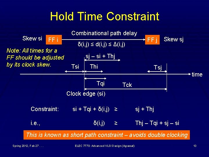
Hold Time Constraint Skew si FF i Note: All times for a FF should be adjusted by its clock skew. Combinational path delay δ(i, j) ≤ d(i, j) ≤ Δ(i, j) FF j Skew sj sj – si + Thj Tsi Thi Tsj time Tqi Tck Clock edge (si) Constraint: i. e. , si + Tqi + δ(i, j) ≥ sj + Thj – Tqi + sj – si This is known as short path constraint – avoids double clocking Spring 2012, Feb 27. . . ELEC 7770: Advanced VLSI Design (Agrawal) 13

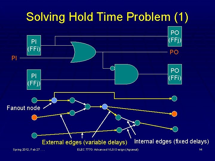
Solving Hold Time Problem (1) PO (FFj) PI (FFi) PO PI PO (FFi) PI (FFj) Fanout node External edges (variable delays) Spring 2012, Feb 27. . . Internal edges (fixed delays) ELEC 7770: Advanced VLSI Design (Agrawal) 14

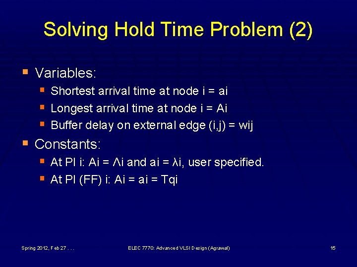
Solving Hold Time Problem (2) § Variables: § Shortest arrival time at node i = ai § Longest arrival time at node i = Ai § Buffer delay on external edge (i, j) = wij § Constants: § At PI i: Ai = Λi and ai = λi, user specified. § At PI (FF) i: Ai = ai = Tqi Spring 2012, Feb 27. . . ELEC 7770: Advanced VLSI Design (Agrawal) 15

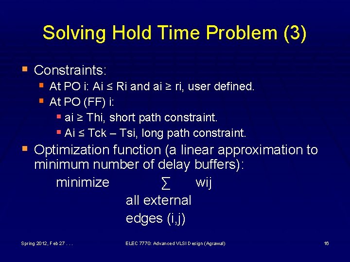
Solving Hold Time Problem (3) § Constraints: § At PO i: Ai ≤ Ri and ai ≥ ri, user defined. § At PO (FF) i: § ai ≥ Thi, short path constraint. § Ai ≤ Tck – Tsi, long path constraint. § Optimization function (a linear approximation to minimum number of delay buffers): minimize ∑ wij all external edges (i, j) Spring 2012, Feb 27. . . ELEC 7770: Advanced VLSI Design (Agrawal) 16

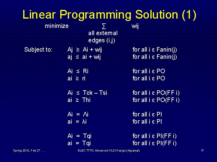
Linear Programming Solution (1) minimize Subject to: Spring 2012, Feb 27. . . ∑ all external edges (i, j) Aj ≥ Ai + wij aj ≤ ai + wij Ai ≤ Ri ai ≥ ri for all i ε PO Ai ≤ Tck – Tsi ai ≥ Thi for all i ε PO(FF i) Ai = Λi ai = λi for all i ε PI Ai = Tqi ai = Tqi for all i ε PI(FF i) for all i ε Fanin(j) ELEC 7770: Advanced VLSI Design (Agrawal) 17

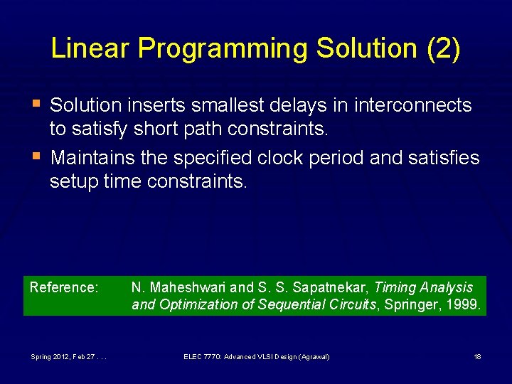
Linear Programming Solution (2) § Solution inserts smallest delays in interconnects § to satisfy short path constraints. Maintains the specified clock period and satisfies setup time constraints. Reference: Spring 2012, Feb 27. . . N. Maheshwari and S. S. Sapatnekar, Timing Analysis and Optimization of Sequential Circuits, Springer, 1999. ELEC 7770: Advanced VLSI Design (Agrawal) 18

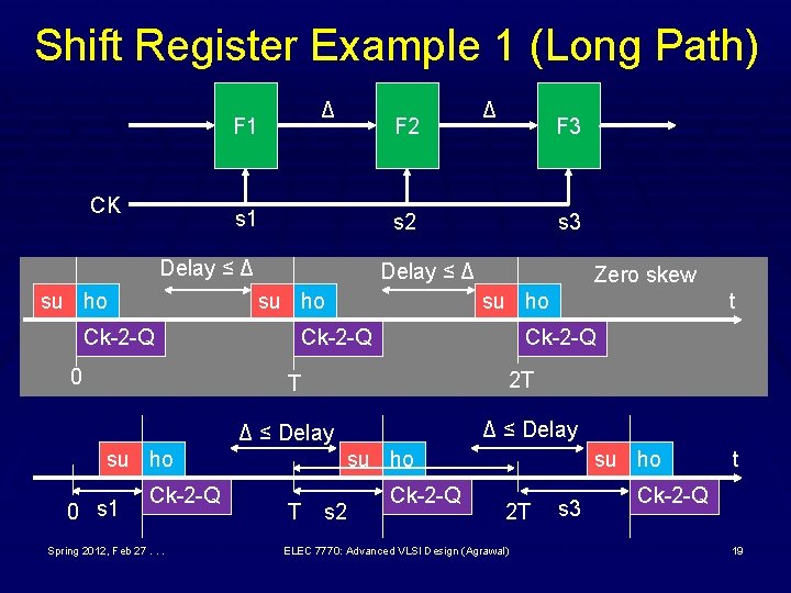
Shift Register Example 1 (Long Path) Δ F 1 CK F 2 s 1 0 Ck-2 -Q su ho Spring 2012, Feb 27. . . t Ck-2 -Q 2 T Δ ≤ Delay Ck-2 -Q Zero skew su ho T 0 s 1 s 3 Delay ≤ Δ su ho Ck-2 -Q F 3 s 2 Delay ≤ Δ su ho T s 2 Ck-2 -Q su ho 2 T ELEC 7770: Advanced VLSI Design (Agrawal) s 3 t Ck-2 -Q 19

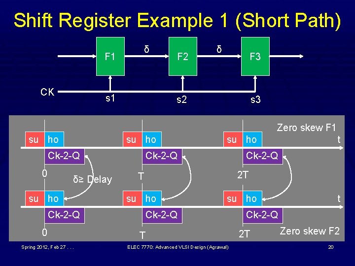
Shift Register Example 1 (Short Path) F 1 CK δ s 1 F 2 δ F 3 s 2 s 3 Zero skew F 1 su ho Ck-2 -Q 0 δ≥ Delay su ho Ck-2 -Q 0 Spring 2012, Feb 27. . . su ho Ck-2 -Q t Ck-2 -Q T 2 T su ho Ck-2 -Q T ELEC 7770: Advanced VLSI Design (Agrawal) t Ck-2 -Q 2 T Zero skew F 2 20

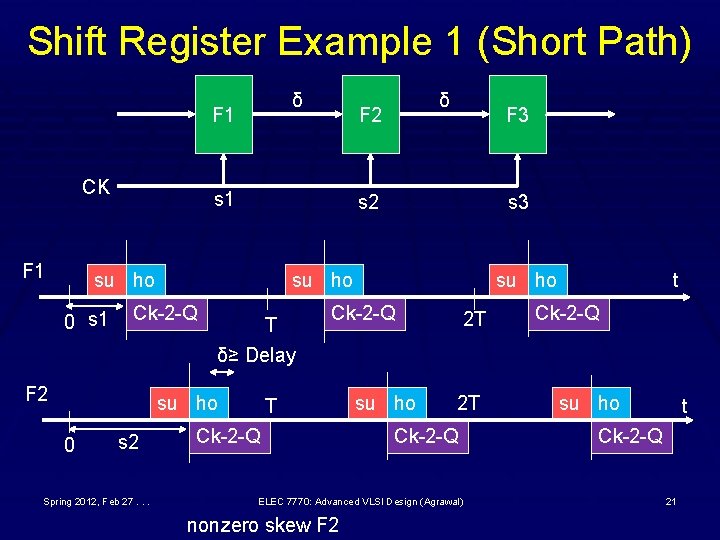
Shift Register Example 1 (Short Path) δ F 1 CK F 1 s 2 T δ≥ Delay su ho s 2 Spring 2012, Feb 27. . . F 3 su ho Ck-2 -Q F 2 0 F 2 s 1 su ho 0 s 1 δ su ho Ck-2 -Q T Ck-2 -Q su ho 2 T 2 T Ck-2 -Q ELEC 7770: Advanced VLSI Design (Agrawal) nonzero skew F 2 t Ck-2 -Q su ho t Ck-2 -Q 21

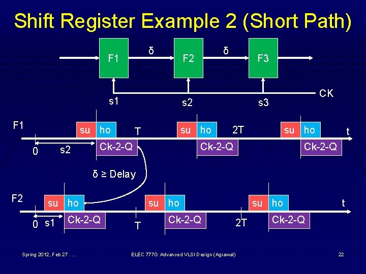
Shift Register Example 2 (Short Path) δ F 1 F 2 s 1 F 1 s 2 F 3 s 2 su ho 0 δ s 3 su ho T Ck-2 -Q CK 2 T su ho Ck-2 -Q t Ck-2 -Q δ ≥ Delay F 2 su ho 0 s 1 Ck-2 -Q Spring 2012, Feb 27. . . su ho T Ck-2 -Q su ho 2 T ELEC 7770: Advanced VLSI Design (Agrawal) t Ck-2 -Q 22

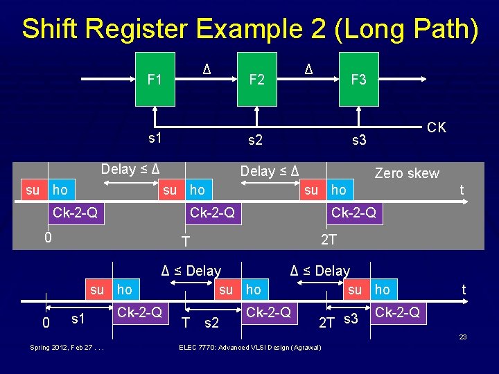
Shift Register Example 2 (Long Path) Δ F 1 s 1 F 2 su ho Ck-2 -Q Zero skew su ho Ck-2 -Q 0 2 T Δ ≤ Delay su ho Ck-2 -Q T t Ck-2 -Q T su ho CK s 3 Delay ≤ Δ su ho s 1 F 3 s 2 Delay ≤ Δ 0 Δ s 2 Δ ≤ Delay su ho Ck-2 -Q 2 T s 3 t Ck-2 -Q 23 Spring 2012, Feb 27. . . ELEC 7770: Advanced VLSI Design (Agrawal)