ELEC 7770 Advanced VLSI Design Spring 2008 VLSI

- Slides: 45

ELEC 7770 Advanced VLSI Design Spring 2008 VLSI Test Principles Vishwani D. Agrawal James J. Danaher Professor ECE Department, Auburn University Auburn, AL 36849 vagrawal@eng. auburn. edu http: //www. eng. auburn. edu/~vagrawal/COURSE/E 7770_Spr 08/course. html Spring 08, Mar 13 ELEC 7770: Advanced VLSI Design (Agrawal) 1

Reference M. L. Bushnell and V. D. Agrawal, Essentials of Electronic Testing for Digital, Memory and Mixed-Signal VLSI Circuits, Springer, 2000. Spring 08, Mar 13 ELEC 7770: Advanced VLSI Design (Agrawal) 2

Testing and Diagnosis § Testing § Determine whether of not a device is faulty. § Accomplished through input-output experiment. § Diagnosis § Given a device has failed, locate the fault that caused § failure Accomplished by analysis of test data and by intrusive experiments. Spring 08, Mar 13 ELEC 7770: Advanced VLSI Design (Agrawal) 3

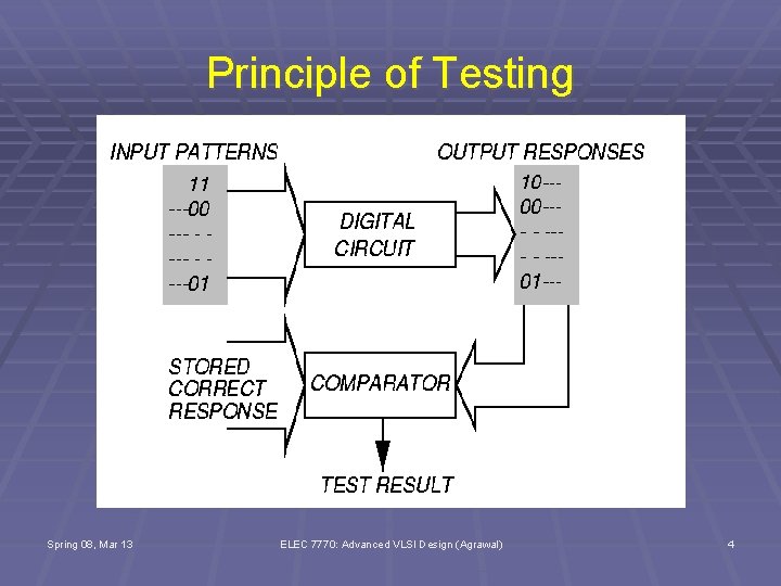
Principle of Testing Spring 08, Mar 13 ELEC 7770: Advanced VLSI Design (Agrawal) 4

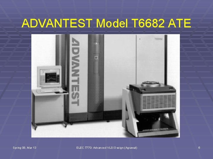
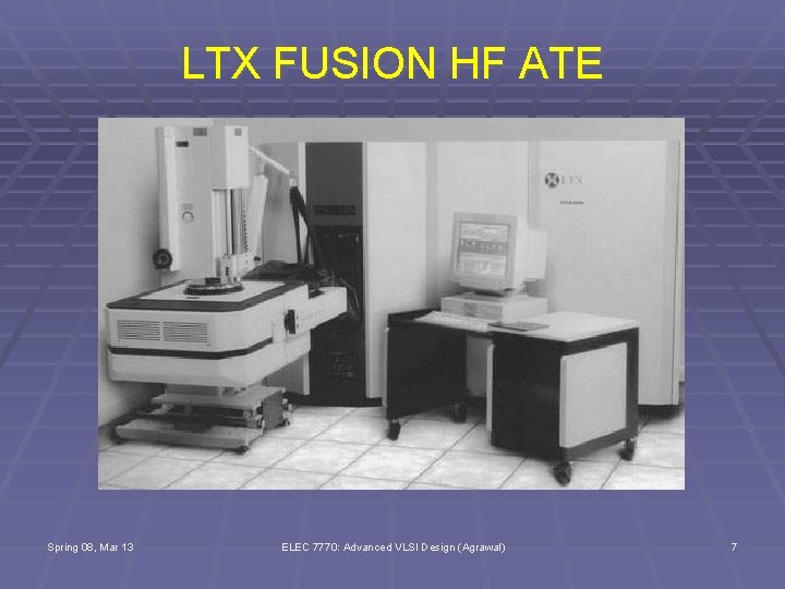
Automatic Test Equipment (ATE) § Consists of: § Powerful computer § Powerful 32 -bit Digital Signal Processor (DSP) § § § for analog testing Test Program (written in high-level language) running on the computer Probe Head (actually touches the bare or packaged chip to perform fault detection experiments) Probe Card or Membrane Probe (contains electronics to measure signals on chip pin or pad) Spring 08, Mar 13 ELEC 7770: Advanced VLSI Design (Agrawal) 5

ADVANTEST Model T 6682 ATE Spring 08, Mar 13 ELEC 7770: Advanced VLSI Design (Agrawal) 6

LTX FUSION HF ATE Spring 08, Mar 13 ELEC 7770: Advanced VLSI Design (Agrawal) 7

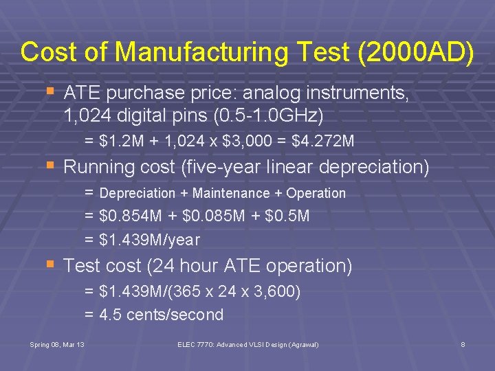
Cost of Manufacturing Test (2000 AD) § ATE purchase price: analog instruments, 1, 024 digital pins (0. 5 -1. 0 GHz) = $1. 2 M + 1, 024 x $3, 000 = $4. 272 M § Running cost (five-year linear depreciation) = Depreciation + Maintenance + Operation = $0. 854 M + $0. 085 M + $0. 5 M = $1. 439 M/year § Test cost (24 hour ATE operation) = $1. 439 M/(365 x 24 x 3, 600) = 4. 5 cents/second Spring 08, Mar 13 ELEC 7770: Advanced VLSI Design (Agrawal) 8

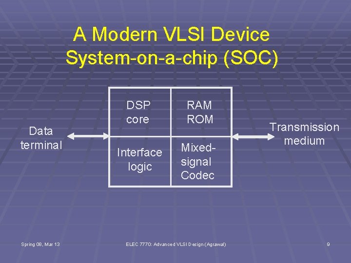
A Modern VLSI Device System-on-a-chip (SOC) Data terminal Spring 08, Mar 13 DSP core RAM ROM Interface logic Mixedsignal Codec ELEC 7770: Advanced VLSI Design (Agrawal) Transmission medium 9

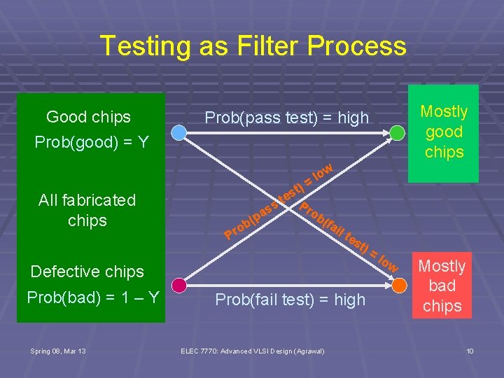
Testing as Filter Process Good chips Prob(good) = Y Mostly good chips Prob(pass test) = high ow l = All fabricated chips t) s te P s ro as b( p ( fai b lt ro P es t) Defective chips Prob(bad) = 1 – Y Spring 08, Mar 13 Prob(fail test) = high ELEC 7770: Advanced VLSI Design (Agrawal) =l ow Mostly bad chips 10

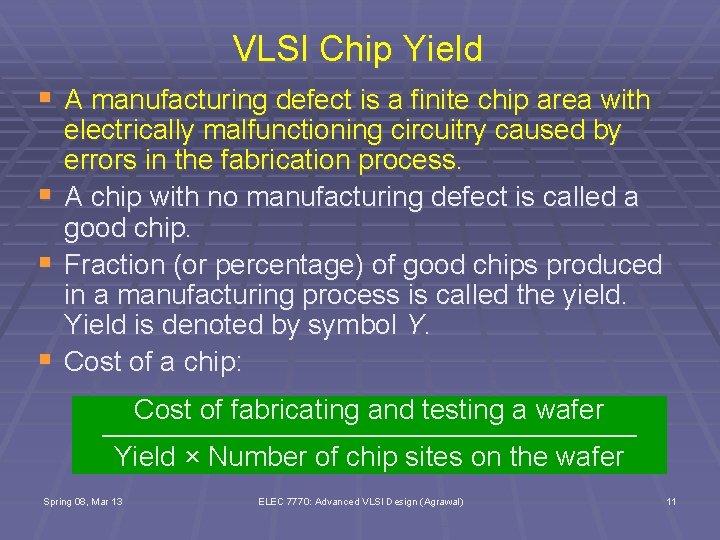
VLSI Chip Yield § A manufacturing defect is a finite chip area with § § § electrically malfunctioning circuitry caused by errors in the fabrication process. A chip with no manufacturing defect is called a good chip. Fraction (or percentage) of good chips produced in a manufacturing process is called the yield. Yield is denoted by symbol Y. Cost of a chip: Cost of fabricating and testing a wafer Yield × Number of chip sites on the wafer Spring 08, Mar 13 ELEC 7770: Advanced VLSI Design (Agrawal) 11

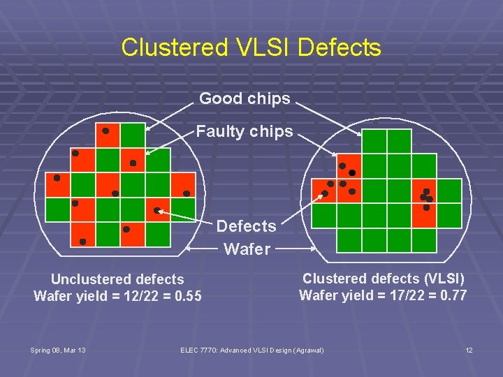
Clustered VLSI Defects Good chips Faulty chips Defects Wafer Unclustered defects Wafer yield = 12/22 = 0. 55 Spring 08, Mar 13 Clustered defects (VLSI) Wafer yield = 17/22 = 0. 77 ELEC 7770: Advanced VLSI Design (Agrawal) 12

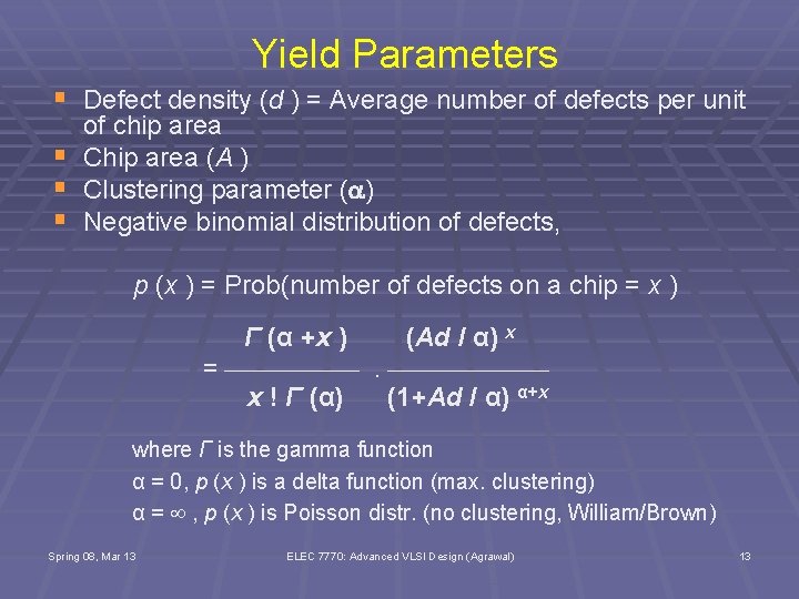
Yield Parameters § Defect density (d ) = Average number of defects per unit § § § of chip area Chip area (A ) Clustering parameter (a) Negative binomial distribution of defects, p (x ) = Prob(number of defects on a chip = x ) Γ (α +x ) (Ad / α) x = . x ! Γ (α) (1+Ad / α) α+x where Γ is the gamma function α = 0, p (x ) is a delta function (max. clustering) α = , p (x ) is Poisson distr. (no clustering, William/Brown) Spring 08, Mar 13 ELEC 7770: Advanced VLSI Design (Agrawal) 13

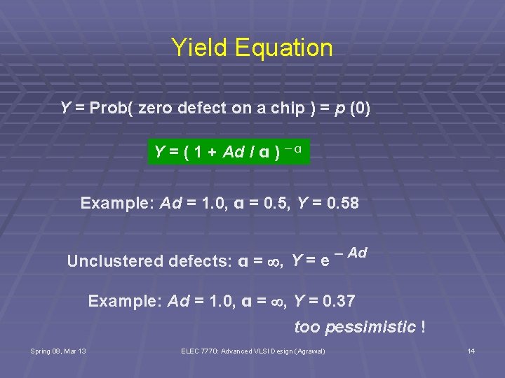
Yield Equation Y = Prob( zero defect on a chip ) = p (0) Y = ( 1 + Ad / α ) – α Example: Ad = 1. 0, α = 0. 5, Y = 0. 58 Unclustered defects: α = , Y = e – Ad Example: Ad = 1. 0, α = , Y = 0. 37 too pessimistic ! Spring 08, Mar 13 ELEC 7770: Advanced VLSI Design (Agrawal) 14

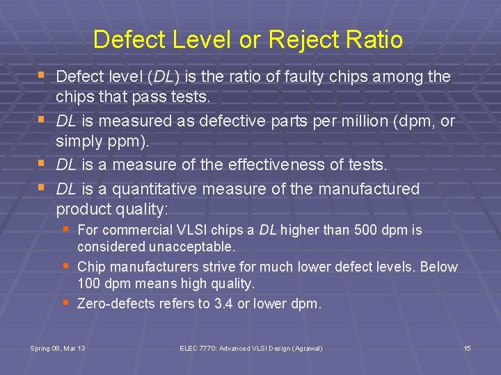
Defect Level or Reject Ratio § Defect level (DL) is the ratio of faulty chips among the § § § chips that pass tests. DL is measured as defective parts per million (dpm, or simply ppm). DL is a measure of the effectiveness of tests. DL is a quantitative measure of the manufactured product quality: § For commercial VLSI chips a DL higher than 500 dpm is § § considered unacceptable. Chip manufacturers strive for much lower defect levels. Below 100 dpm means high quality. Zero-defects refers to 3. 4 or lower dpm. Spring 08, Mar 13 ELEC 7770: Advanced VLSI Design (Agrawal) 15

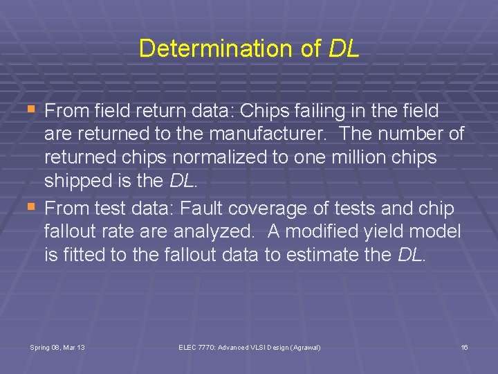
Determination of DL § From field return data: Chips failing in the field § are returned to the manufacturer. The number of returned chips normalized to one million chips shipped is the DL. From test data: Fault coverage of tests and chip fallout rate are analyzed. A modified yield model is fitted to the fallout data to estimate the DL. Spring 08, Mar 13 ELEC 7770: Advanced VLSI Design (Agrawal) 16

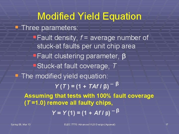
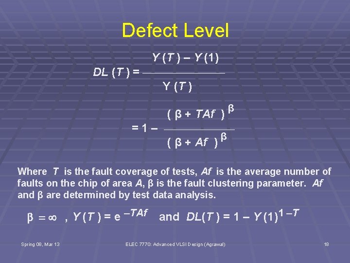
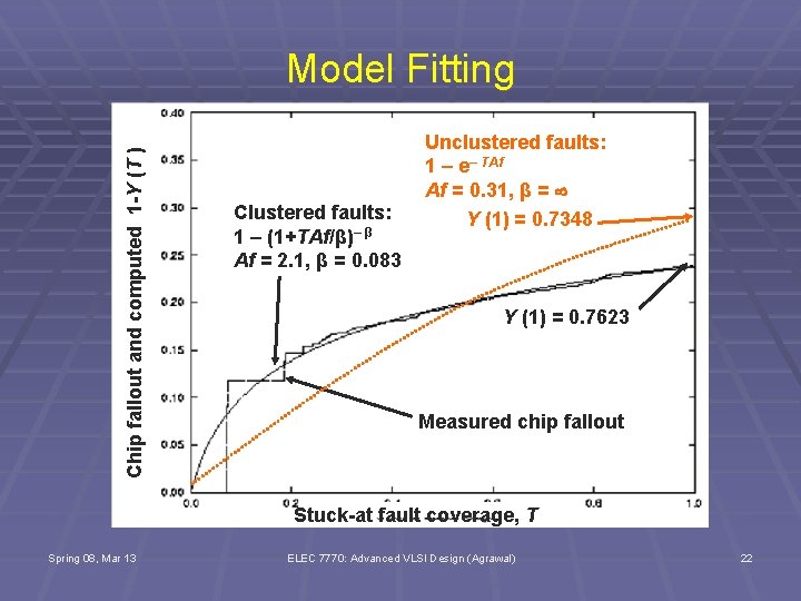
Modified Yield Equation § Three parameters: § Fault density, f = average number of § stuck-at faults per unit chip area § Fault clustering parameter, b § Stuck-at fault coverage, T The modified yield equation: Y (T ) = (1 + TAf / β) – β Assuming that tests with 100% fault coverage (T =1. 0) remove all faulty chips, Y = Y (1) = (1 + Af / β) – β Spring 08, Mar 13 ELEC 7770: Advanced VLSI Design (Agrawal) 17

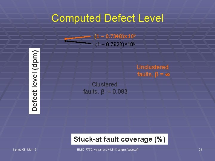
Defect Level Y (T ) – Y (1) DL (T ) = Y (T ) ( β + TAf ) =1– β ( β + Af ) β Where T is the fault coverage of tests, Af is the average number of faults on the chip of area A, β is the fault clustering parameter. Af and β are determined by test data analysis. b = , Y (T ) = e –TAf Spring 08, Mar 13 and DL(T ) = 1 – Y (1)1 –T ELEC 7770: Advanced VLSI Design (Agrawal) 18

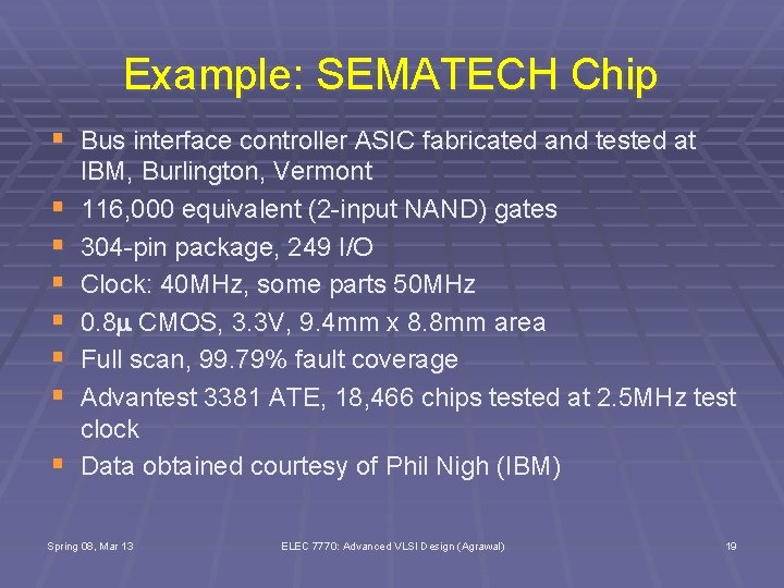
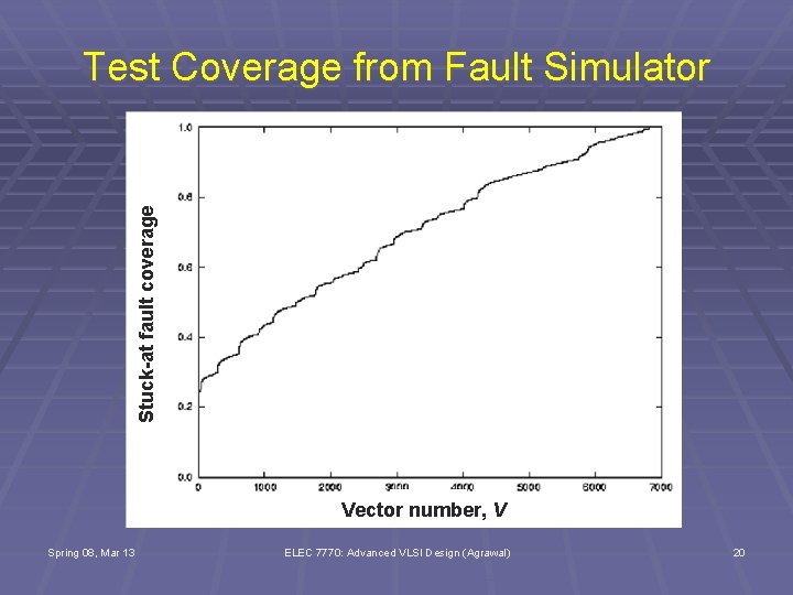
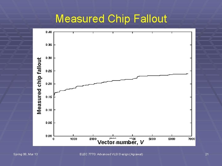
Example: SEMATECH Chip § Bus interface controller ASIC fabricated and tested at § § § § IBM, Burlington, Vermont 116, 000 equivalent (2 -input NAND) gates 304 -pin package, 249 I/O Clock: 40 MHz, some parts 50 MHz 0. 8 m CMOS, 3. 3 V, 9. 4 mm x 8. 8 mm area Full scan, 99. 79% fault coverage Advantest 3381 ATE, 18, 466 chips tested at 2. 5 MHz test clock Data obtained courtesy of Phil Nigh (IBM) Spring 08, Mar 13 ELEC 7770: Advanced VLSI Design (Agrawal) 19

Stuck-at fault coverage Test Coverage from Fault Simulator Vector number, V Spring 08, Mar 13 ELEC 7770: Advanced VLSI Design (Agrawal) 20

Measured chip fallout Measured Chip Fallout Vector number, V Spring 08, Mar 13 ELEC 7770: Advanced VLSI Design (Agrawal) 21

Chip fallout and computed 1 -Y (T ) Model Fitting Clustered faults: 1 – (1+TAf/β)– β Af = 2. 1, β = 0. 083 Unclustered faults: 1 – e– TAf Af = 0. 31, β = Y (1) = 0. 7348 Y (1) = 0. 7623 Measured chip fallout Stuck-at fault coverage, T Spring 08, Mar 13 ELEC 7770: Advanced VLSI Design (Agrawal) 22

Computed Defect Level Defect level (dpm) (1 – 0. 7348)× 106 (1 – 0. 7623)× 106 Unclustered faults, β = Clustered faults, β = 0. 083 Stuck-at fault coverage (%) Spring 08, Mar 13 ELEC 7770: Advanced VLSI Design (Agrawal) 23

Fault Modeling Spring 08, Mar 13 ELEC 7770: Advanced VLSI Design (Agrawal) 24

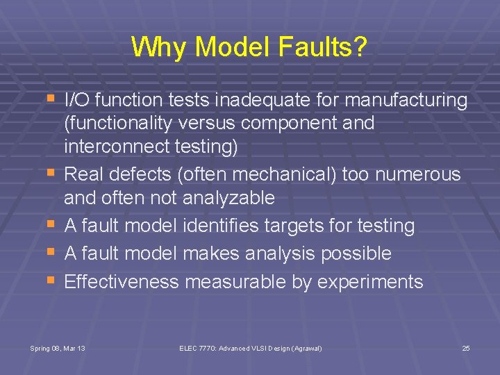
Why Model Faults? § I/O function tests inadequate for manufacturing § § (functionality versus component and interconnect testing) Real defects (often mechanical) too numerous and often not analyzable A fault model identifies targets for testing A fault model makes analysis possible Effectiveness measurable by experiments Spring 08, Mar 13 ELEC 7770: Advanced VLSI Design (Agrawal) 25

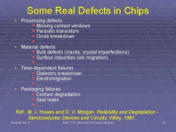
Some Real Defects in Chips § Processing defects § Missing contact windows § Parasitic transistors § Oxide breakdown §. . . § Material defects § Bulk defects (cracks, crystal imperfections) § Surface impurities (ion migration) §. . . § Time-dependent failures § Dielectric breakdown § Electromigration §. . . § Packaging failures § Contact degradation § Seal leaks §. . . Ref. : M. J. Howes and D. V. Morgan, Reliability and Degradation Semiconductor Devices and Circuits, Wiley, 1981. Spring 08, Mar 13 ELEC 7770: Advanced VLSI Design (Agrawal) 26

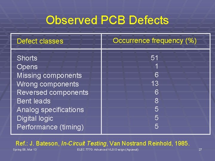
Observed PCB Defects Occurrence frequency (%) Defect classes Shorts Opens Missing components Wrong components Reversed components Bent leads Analog specifications Digital logic Performance (timing) 51 1 6 13 6 8 5 5 5 Ref. : J. Bateson, In-Circuit Testing, Van Nostrand Reinhold, 1985. Spring 08, Mar 13 ELEC 7770: Advanced VLSI Design (Agrawal) 27

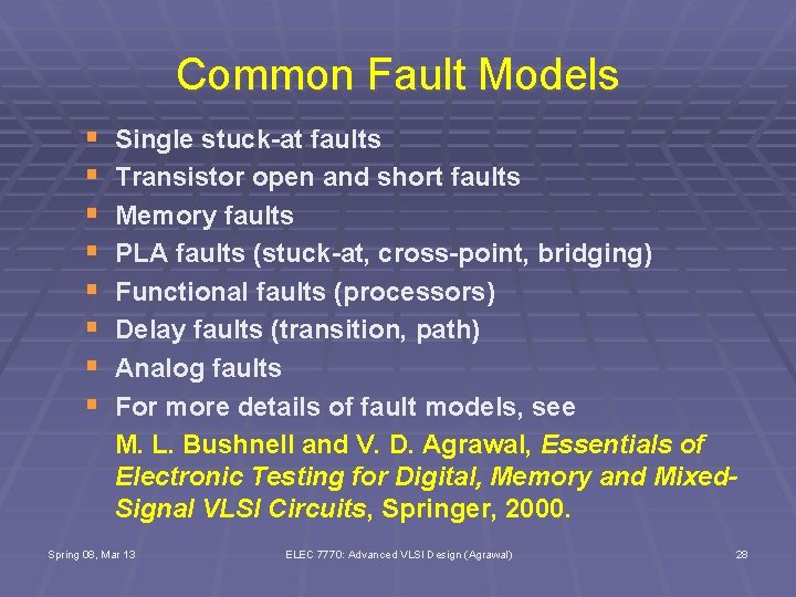
Common Fault Models § § § § Single stuck-at faults Transistor open and short faults Memory faults PLA faults (stuck-at, cross-point, bridging) Functional faults (processors) Delay faults (transition, path) Analog faults For more details of fault models, see M. L. Bushnell and V. D. Agrawal, Essentials of Electronic Testing for Digital, Memory and Mixed. Signal VLSI Circuits, Springer, 2000. Spring 08, Mar 13 ELEC 7770: Advanced VLSI Design (Agrawal) 28

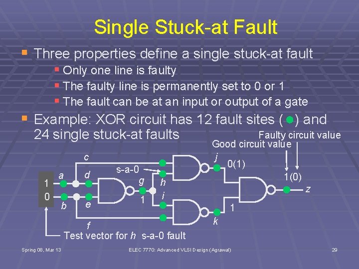
Single Stuck-at Fault § Three properties define a single stuck-at fault § § Only one line is faulty § The faulty line is permanently set to 0 or 1 § The fault can be at an input or output of a gate Example: XOR circuit has 12 fault sites ( ) and Faulty circuit value 24 single stuck-at faults c 1 0 a b d e s-a-0 g 1 h i f Test vector for h s-a-0 fault Spring 08, Mar 13 Good circuit value j 0(1) 1(0) z 1 k ELEC 7770: Advanced VLSI Design (Agrawal) 29

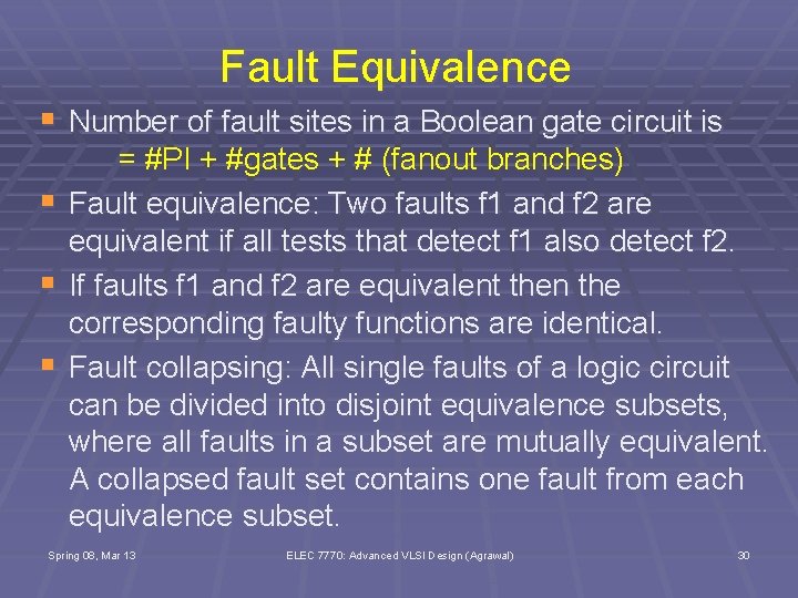
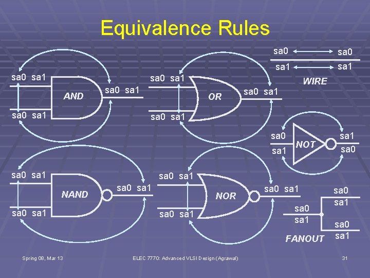
Fault Equivalence § Number of fault sites in a Boolean gate circuit is § § § = #PI + #gates + # (fanout branches) Fault equivalence: Two faults f 1 and f 2 are equivalent if all tests that detect f 1 also detect f 2. If faults f 1 and f 2 are equivalent then the corresponding faulty functions are identical. Fault collapsing: All single faults of a logic circuit can be divided into disjoint equivalence subsets, where all faults in a subset are mutually equivalent. A collapsed fault set contains one fault from each equivalence subset. Spring 08, Mar 13 ELEC 7770: Advanced VLSI Design (Agrawal) 30

Equivalence Rules sa 0 sa 1 sa 0 sa 1 AND sa 0 sa 1 OR WIRE sa 0 sa 1 NOT sa 1 sa 0 sa 1 NAND sa 0 sa 1 NOR sa 0 sa 1 FANOUT Spring 08, Mar 13 ELEC 7770: Advanced VLSI Design (Agrawal) sa 0 sa 1 31

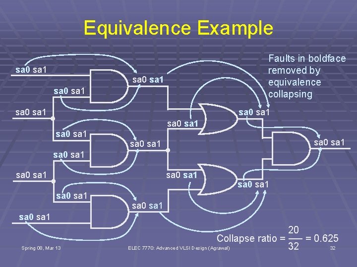
Equivalence Example Faults in boldface removed by equivalence collapsing sa 0 sa 1 sa 0 sa 1 sa 0 sa 1 sa 0 sa 1 Spring 08, Mar 13 20 Collapse ratio = ── = 0. 625 ELEC 7770: Advanced VLSI Design (Agrawal) 32 32

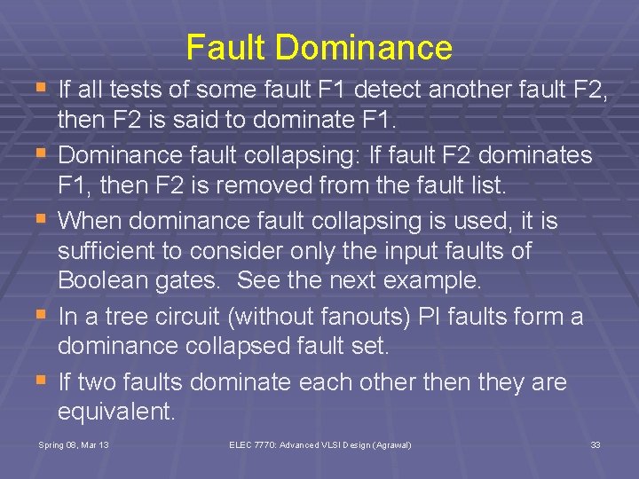
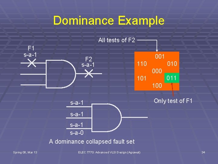
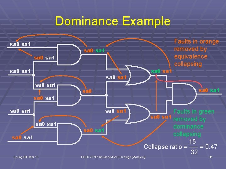
Fault Dominance § If all tests of some fault F 1 detect another fault F 2, § § then F 2 is said to dominate F 1. Dominance fault collapsing: If fault F 2 dominates F 1, then F 2 is removed from the fault list. When dominance fault collapsing is used, it is sufficient to consider only the input faults of Boolean gates. See the next example. In a tree circuit (without fanouts) PI faults form a dominance collapsed fault set. If two faults dominate each other then they are equivalent. Spring 08, Mar 13 ELEC 7770: Advanced VLSI Design (Agrawal) 33

Dominance Example All tests of F 2 F 1 s-a-1 F 2 s-a-1 001 110 000 011 100 s-a-1 Only test of F 1 s-a-1 s-a-0 A dominance collapsed fault set Spring 08, Mar 13 ELEC 7770: Advanced VLSI Design (Agrawal) 34

Dominance Example sa 0 sa 1 Faults in orange removed by equivalence collapsing sa 0 sa 1 sa 0 sa 1 sa 0 sa 1 sa 0 sa 1 Spring 08, Mar 13 sa 0 sa 1 Faults in green sa 0 sa 1 removed by dominance collapsing 15 Collapse ratio = ── = 0. 47 32 ELEC 7770: Advanced VLSI Design (Agrawal) 35

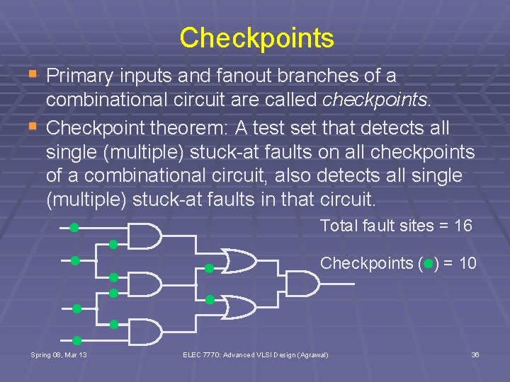
Checkpoints § Primary inputs and fanout branches of a § combinational circuit are called checkpoints. Checkpoint theorem: A test set that detects all single (multiple) stuck-at faults on all checkpoints of a combinational circuit, also detects all single (multiple) stuck-at faults in that circuit. Total fault sites = 16 Checkpoints ( ) = 10 Spring 08, Mar 13 ELEC 7770: Advanced VLSI Design (Agrawal) 36

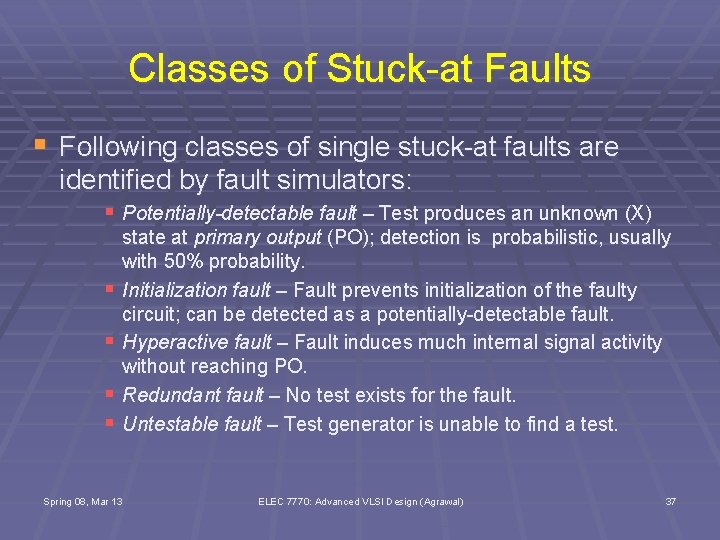
Classes of Stuck-at Faults § Following classes of single stuck-at faults are identified by fault simulators: § Potentially-detectable fault – Test produces an unknown (X) § § state at primary output (PO); detection is probabilistic, usually with 50% probability. Initialization fault – Fault prevents initialization of the faulty circuit; can be detected as a potentially-detectable fault. Hyperactive fault – Fault induces much internal signal activity without reaching PO. Redundant fault – No test exists for the fault. Untestable fault – Test generator is unable to find a test. Spring 08, Mar 13 ELEC 7770: Advanced VLSI Design (Agrawal) 37

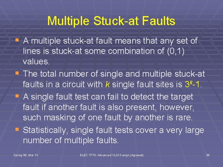
Multiple Stuck-at Faults § A multiple stuck-at fault means that any set of § § § lines is stuck-at some combination of (0, 1) values. The total number of single and multiple stuck-at faults in a circuit with k single fault sites is 3 k-1. A single fault test can fail to detect the target fault if another fault is also present, however, such masking of one fault by another is rare. Statistically, single fault tests cover a very large number of multiple faults. Spring 08, Mar 13 ELEC 7770: Advanced VLSI Design (Agrawal) 38

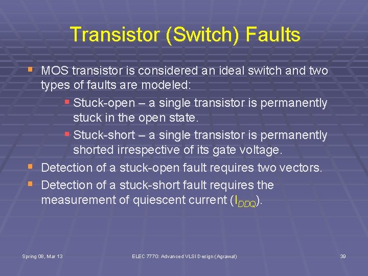
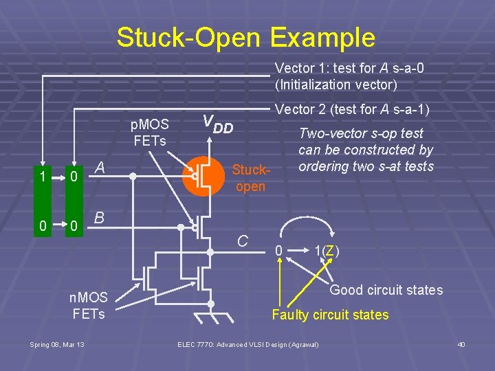
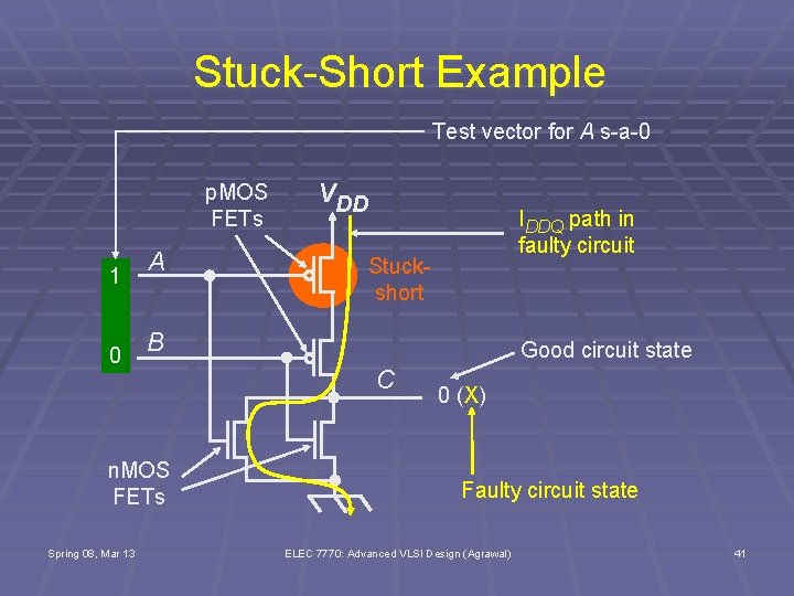
Transistor (Switch) Faults § MOS transistor is considered an ideal switch and two § § types of faults are modeled: § Stuck-open – a single transistor is permanently stuck in the open state. § Stuck-short – a single transistor is permanently shorted irrespective of its gate voltage. Detection of a stuck-open fault requires two vectors. Detection of a stuck-short fault requires the measurement of quiescent current (IDDQ). Spring 08, Mar 13 ELEC 7770: Advanced VLSI Design (Agrawal) 39

Stuck-Open Example Vector 1: test for A s-a-0 (Initialization vector) p. MOS FETs 1 0 0 0 A VDD Two-vector s-op test can be constructed by ordering two s-at tests Stuckopen B n. MOS FETs Spring 08, Mar 13 Vector 2 (test for A s-a-1) C 0 1(Z) Good circuit states Faulty circuit states ELEC 7770: Advanced VLSI Design (Agrawal) 40

Stuck-Short Example Test vector for A s-a-0 p. MOS FETs 1 0 A IDDQ path in faulty circuit Stuckshort B n. MOS FETs Spring 08, Mar 13 VDD Good circuit state C 0 (X) Faulty circuit state ELEC 7770: Advanced VLSI Design (Agrawal) 41

Summary § Fault models are analyzable approximations of defects § § and are essential for a test methodology. For digital logic single stuck-at fault model offers best advantage of tools and experience. Many other faults (bridging, stuck-open and multiple stuck -at) are largely covered by stuck-at fault tests. Stuck-short and delay faults and technology-dependent faults require special tests. Memory and analog circuits need other specialized fault models and tests. Spring 08, Mar 13 ELEC 7770: Advanced VLSI Design (Agrawal) 42

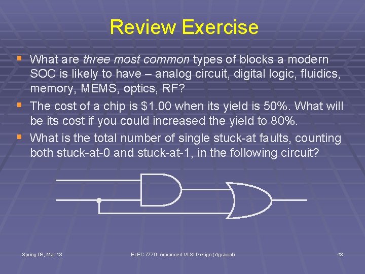
Review Exercise § What are three most common types of blocks a modern § § SOC is likely to have – analog circuit, digital logic, fluidics, memory, MEMS, optics, RF? The cost of a chip is $1. 00 when its yield is 50%. What will be its cost if you could increased the yield to 80%. What is the total number of single stuck-at faults, counting both stuck-at-0 and stuck-at-1, in the following circuit? Spring 08, Mar 13 ELEC 7770: Advanced VLSI Design (Agrawal) 43

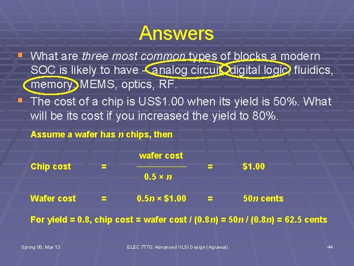
Answers § What are three most common types of blocks a modern § SOC is likely to have – analog circuit, digital logic, fluidics, memory, MEMS, optics, RF. The cost of a chip is US$1. 00 when its yield is 50%. What will be its cost if you increased the yield to 80%. Assume a wafer has n chips, then Chip cost = wafer cost ──── 0. 5 × n Wafer cost = 0. 5 n × $1. 00 = 50 n cents For yield = 0. 8, chip cost = wafer cost / (0. 8 n) = 50 n / (0. 8 n) = 62. 5 cents Spring 08, Mar 13 ELEC 7770: Advanced VLSI Design (Agrawal) 44

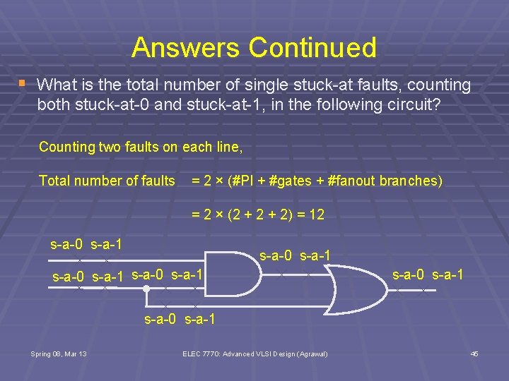
Answers Continued § What is the total number of single stuck-at faults, counting both stuck-at-0 and stuck-at-1, in the following circuit? Counting two faults on each line, Total number of faults = 2 × (#PI + #gates + #fanout branches) = 2 × (2 + 2) = 12 s-a-0 s-a-1 s-a-0 s-a-1 Spring 08, Mar 13 ELEC 7770: Advanced VLSI Design (Agrawal) 45