ELEC 5270 0016270 001 Fall 2006 LowPower Design
- Slides: 37

ELEC 5270 -001/6270 -001 (Fall 2006) Low-Power Design of Electronic Circuits (ELEC 5970/6970) Low Voltage Low Power Devices Vishwani D. Agrawal James J. Danaher Professor Department of Electrical and Computer Engineering Auburn University http: //www. eng. auburn. edu/~vagrawal@eng. auburn. edu 8/29/06 and 8/31/06 ELEC 5270 -001/6270 -001 Lecture 3 1

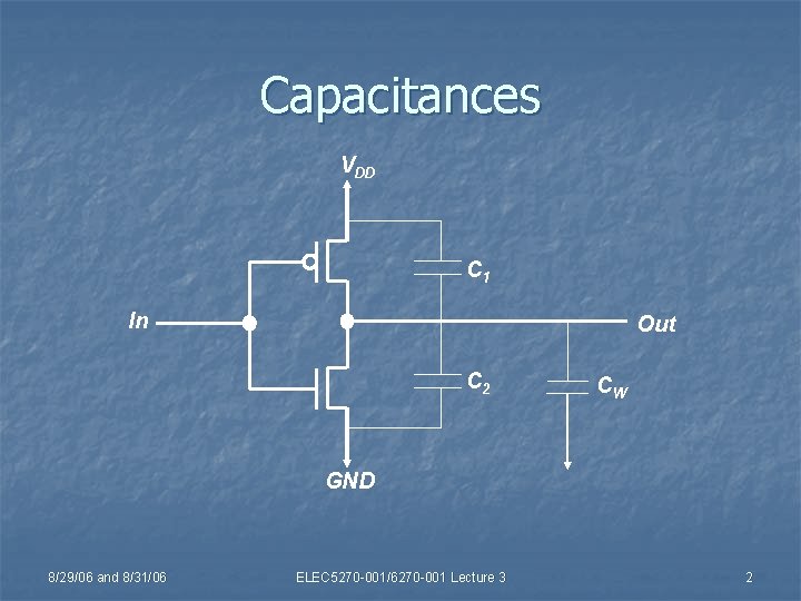
Capacitances VDD C 1 In Out C 2 CW GND 8/29/06 and 8/31/06 ELEC 5270 -001/6270 -001 Lecture 3 2

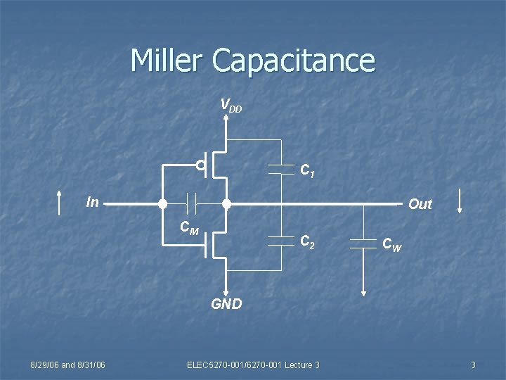
Miller Capacitance VDD C 1 In Out CM C 2 CW GND 8/29/06 and 8/31/06 ELEC 5270 -001/6270 -001 Lecture 3 3

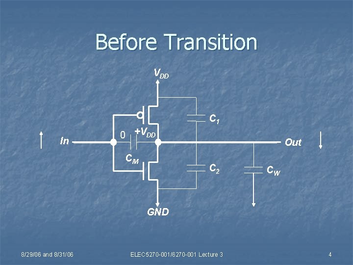
Before Transition VDD C 1 In 0 +VDD CM Out C 2 CW GND 8/29/06 and 8/31/06 ELEC 5270 -001/6270 -001 Lecture 3 4

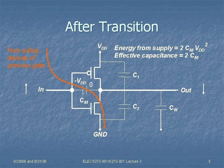
After Transition VDD from pullup devices of previous gate -VDD In 2 Energy from supply = 2 CM VDD Effective capacitance = 2 CM C 1 0 Out CM C 2 CW GND 8/29/06 and 8/31/06 ELEC 5270 -001/6270 -001 Lecture 3 5

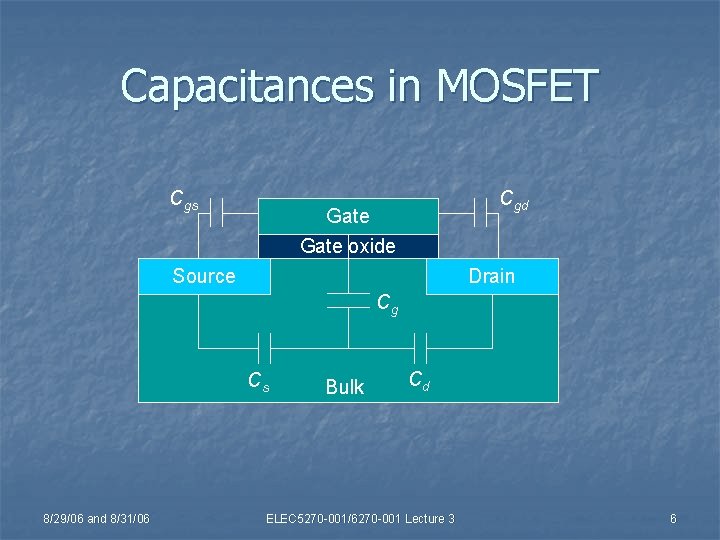
Capacitances in MOSFET Cgs Cgd Gate oxide Source Drain Cg Cs 8/29/06 and 8/31/06 Bulk Cd ELEC 5270 -001/6270 -001 Lecture 3 6

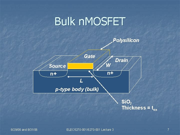
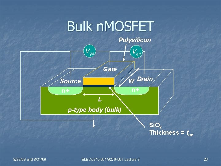
Bulk n. MOSFET Polysilicon Gate W Source Drain n+ n+ L p-type body (bulk) Si. O 2 Thickness = tox 8/29/06 and 8/31/06 ELEC 5270 -001/6270 -001 Lecture 3 7

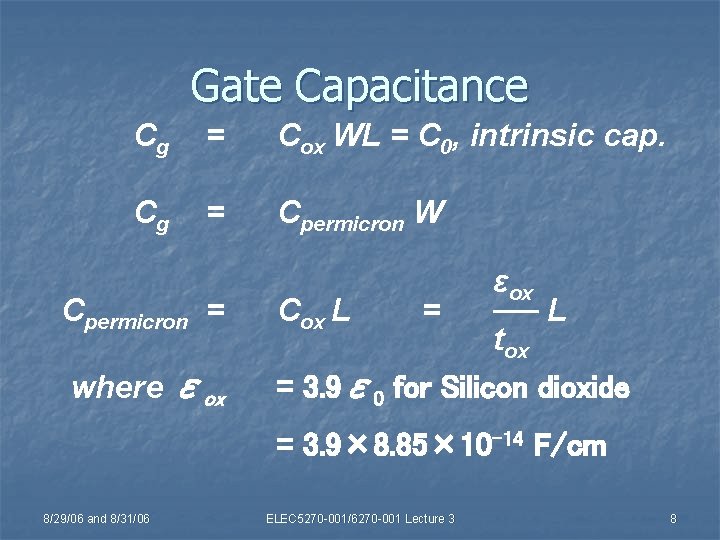
Gate Capacitance Cg = Cox WL = C 0, intrinsic cap. Cg = Cpermicron W Cpermicron = where εox Cox L = ── L tox = 3. 9ε 0 for Silicon dioxide = 3. 9× 8. 85× 10 -14 F/cm 8/29/06 and 8/31/06 ELEC 5270 -001/6270 -001 Lecture 3 8

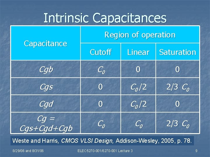
Intrinsic Capacitances Capacitance Region of operation Cutoff Linear Saturation Cgb C 0 0 0 Cgs 0 C 0 /2 2/3 C 0 Cgd 0 C 0 /2 0 Cg = Cgs+Cgd+Cgb C 0 2/3 C 0 Weste and Harris, CMOS VLSI Design, Addison-Wesley, 2005, p. 78. 8/29/06 and 8/31/06 ELEC 5270 -001/6270 -001 Lecture 3 9

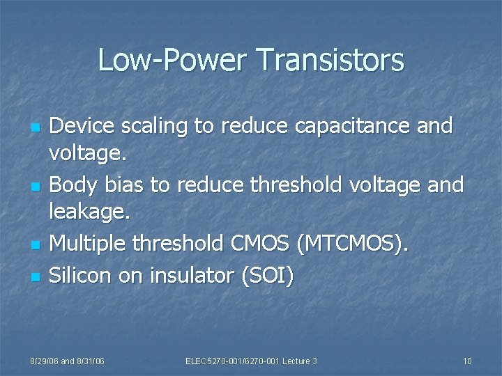
Low-Power Transistors n n Device scaling to reduce capacitance and voltage. Body bias to reduce threshold voltage and leakage. Multiple threshold CMOS (MTCMOS). Silicon on insulator (SOI) 8/29/06 and 8/31/06 ELEC 5270 -001/6270 -001 Lecture 3 10

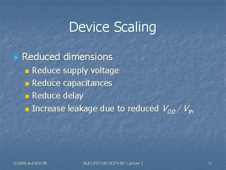
Device Scaling n Reduced dimensions Reduce supply voltage n Reduce capacitances n Reduce delay n Increase leakage due to reduced VDD / Vth n 8/29/06 and 8/31/06 ELEC 5270 -001/6270 -001 Lecture 3 11

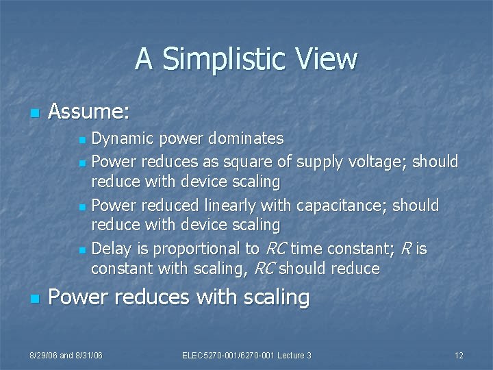
A Simplistic View n Assume: Dynamic power dominates n Power reduces as square of supply voltage; should reduce with device scaling n Power reduced linearly with capacitance; should reduce with device scaling n Delay is proportional to RC time constant; R is constant with scaling, RC should reduce n n Power reduces with scaling 8/29/06 and 8/31/06 ELEC 5270 -001/6270 -001 Lecture 3 12

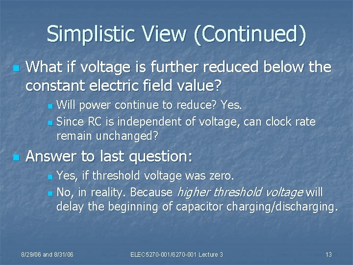
Simplistic View (Continued) n What if voltage is further reduced below the constant electric field value? Will power continue to reduce? Yes. n Since RC is independent of voltage, can clock rate remain unchanged? n n Answer to last question: Yes, if threshold voltage was zero. n No, in reality. Because higher threshold voltage will delay the beginning of capacitor charging/discharging. n 8/29/06 and 8/31/06 ELEC 5270 -001/6270 -001 Lecture 3 13

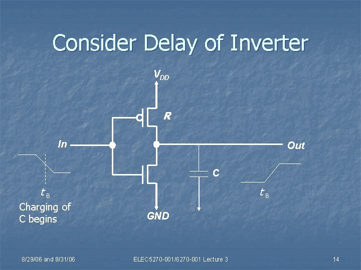
Consider Delay of Inverter VDD R In Out C t. B Charging of C begins 8/29/06 and 8/31/06 t. B GND ELEC 5270 -001/6270 -001 Lecture 3 14

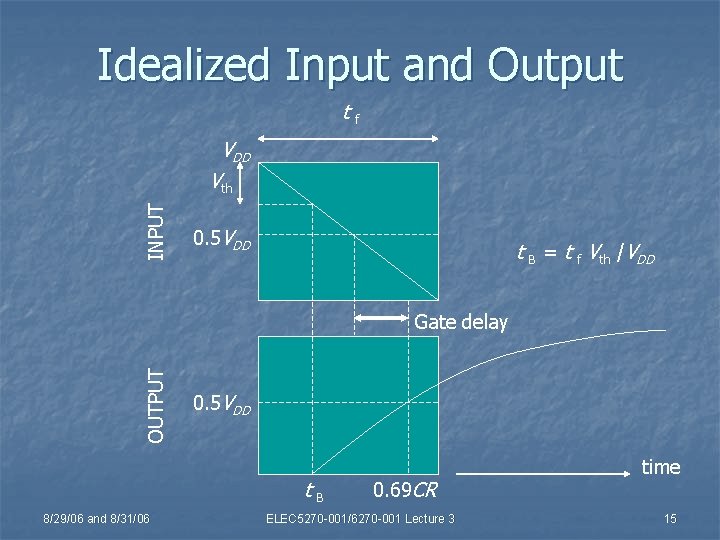
Idealized Input and Output tf INPUT VDD Vth 0. 5 VDD t B = t f Vth /VDD OUTPUT Gate delay 0. 5 VDD t. B 8/29/06 and 8/31/06 0. 69 CR ELEC 5270 -001/6270 -001 Lecture 3 time 15

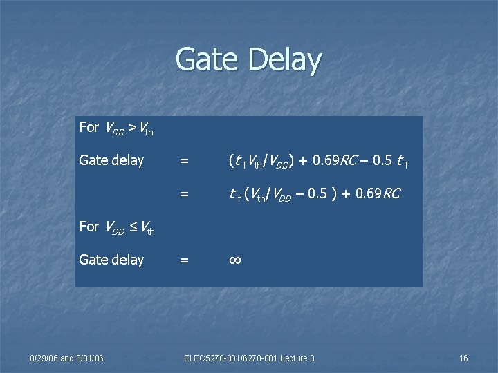
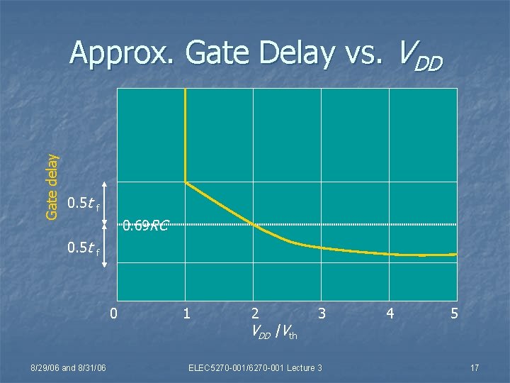
Gate Delay For VDD >Vth Gate delay = (t f. Vth/VDD) + 0. 69 RC – 0. 5 t = t f (Vth/VDD – 0. 5 ) + 0. 69 RC = ∞ f For VDD ≤Vth Gate delay 8/29/06 and 8/31/06 ELEC 5270 -001/6270 -001 Lecture 3 16

Gate delay Approx. Gate Delay vs. VDD 0. 5 t f 0. 69 RC 0. 5 t f 0 8/29/06 and 8/31/06 1 2 VDD /Vth 3 ELEC 5270 -001/6270 -001 Lecture 3 4 5 17

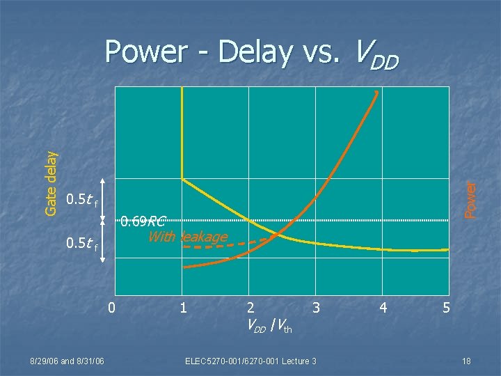
0. 5 t Power Gate delay Power - Delay vs. VDD f 0. 69 RC 0. 5 t With leakage f 0 8/29/06 and 8/31/06 1 2 VDD /Vth 3 ELEC 5270 -001/6270 -001 Lecture 3 4 5 18

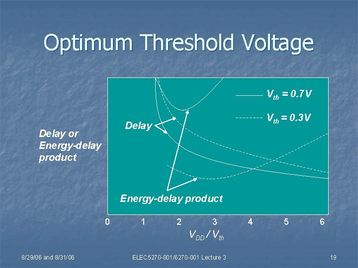
Optimum Threshold Voltage Vth = 0. 7 V Vth = 0. 3 V Delay or Energy-delay product 0 1 2 3 4 5 6 VDD / Vth 8/29/06 and 8/31/06 ELEC 5270 -001/6270 -001 Lecture 3 19

Bulk n. MOSFET Polysilicon Vgs Vgd Gate W Drain n+ Source n+ L p-type body (bulk) Si. O 2 Thickness = tox 8/29/06 and 8/31/06 ELEC 5270 -001/6270 -001 Lecture 3 20

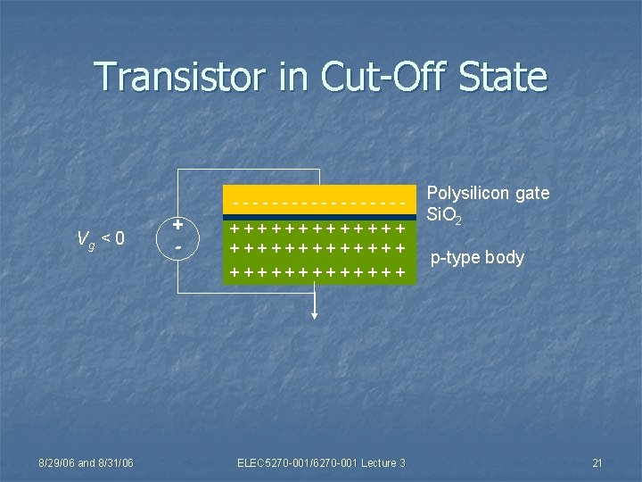
Transistor in Cut-Off State --------- Vg < 0 + - +++++++++++++ 8/29/06 and 8/31/06 ELEC 5270 -001/6270 -001 Lecture 3 Polysilicon gate Si. O 2 p-type body 21

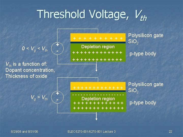
Threshold Voltage, Vth + + + + + 0 < Vg < Vth + - Depletion region +++++++++++++ 8/29/06 and 8/31/06 p-type body +++++++ Vth is a function of: Dopant concentration, Thickness of oxide Vg > Vth Polysilicon gate Si. O 2 + - ---------Depletion region +++++++ ELEC 5270 -001/6270 -001 Lecture 3 Polysilicon gate Si. O 2 p-type body 22

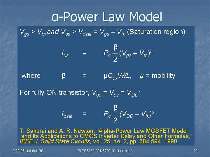
α-Power Law Model Vgs > Vth and Vds > Vdsat = Vgs – Vth (Saturation region): where Ids = β Pc ─ (Vgs – Vth)α 2 β = μCox. W/L, μ = mobility For fully ON transistor, Vgs = Vds = VDD: Idsat = β Pc ─ (VDD – Vth)α 2 T. Sakurai and A. R. Newton, “Alpha-Power Law MOSFET Model and Its Applications to CMOS Inverter Delay and Other Formulas, ” IEEE J. Solid State Circuits, vol. 25, no. 2, pp. 584 -594, 1990. 8/29/06 and 8/31/06 ELEC 5270 -001/6270 -001 Lecture 3 23

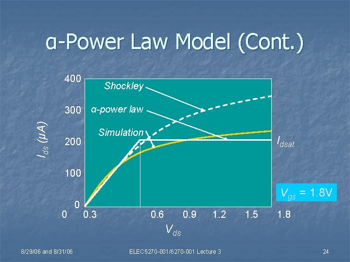
α-Power Law Model (Cont. ) 400 Ids (μA) 300 Shockley α-power law Simulation 200 Idsat 100 0 0 Vgs = 1. 8 V 0. 3 0. 6 0. 9 1. 2 1. 5 1. 8 Vds 8/29/06 and 8/31/06 ELEC 5270 -001/6270 -001 Lecture 3 24

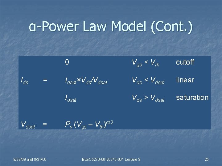
α-Power Law Model (Cont. ) Ids Vdsat = = 8/29/06 and 8/31/06 0 Vgs < Vth cutoff Idsat×Vds/Vdsat Vds < Vdsat linear Idsat Vds > Vdsat saturation Pv (Vgs – Vth)α/2 ELEC 5270 -001/6270 -001 Lecture 3 25

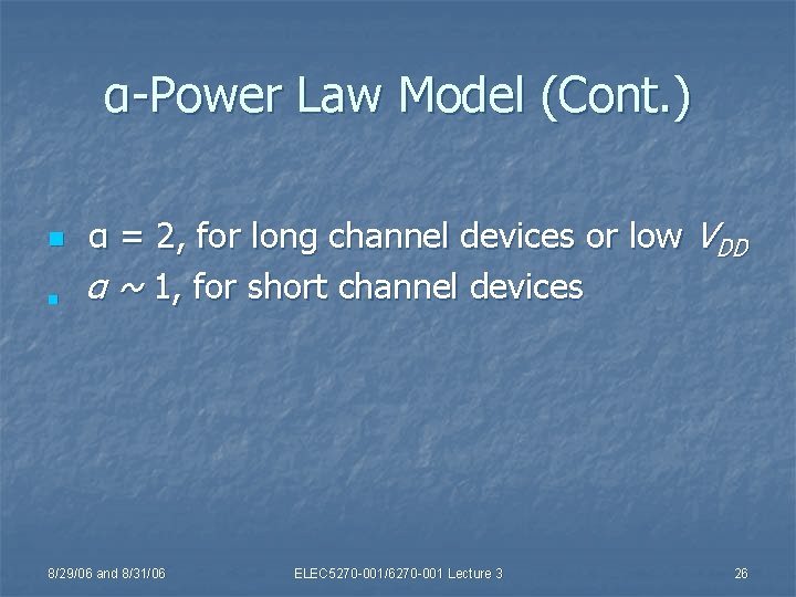
α-Power Law Model (Cont. ) n n α = 2, for long channel devices or low VDD α ~ 1, for short channel devices 8/29/06 and 8/31/06 ELEC 5270 -001/6270 -001 Lecture 3 26

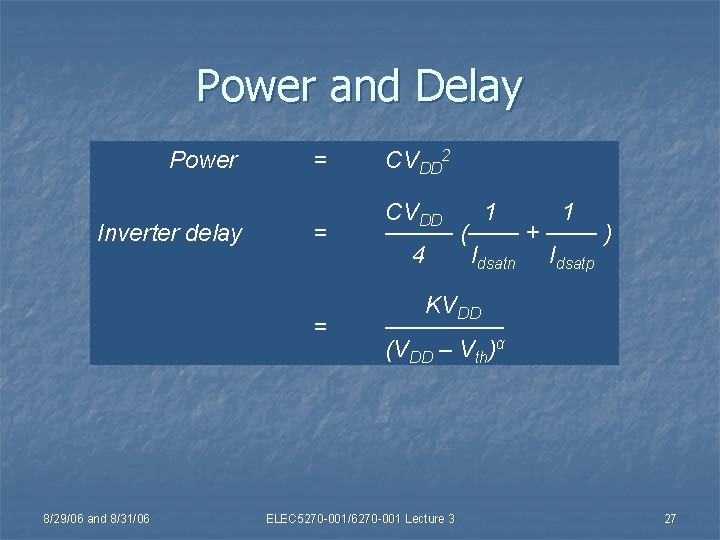
Power and Delay Power Inverter delay 8/29/06 and 8/31/06 = CVDD 2 = CVDD 1 1 ──── (─── + ─── ) 4 Idsatn Idsatp = KVDD ─────── (VDD – Vth)α ELEC 5270 -001/6270 -001 Lecture 3 27

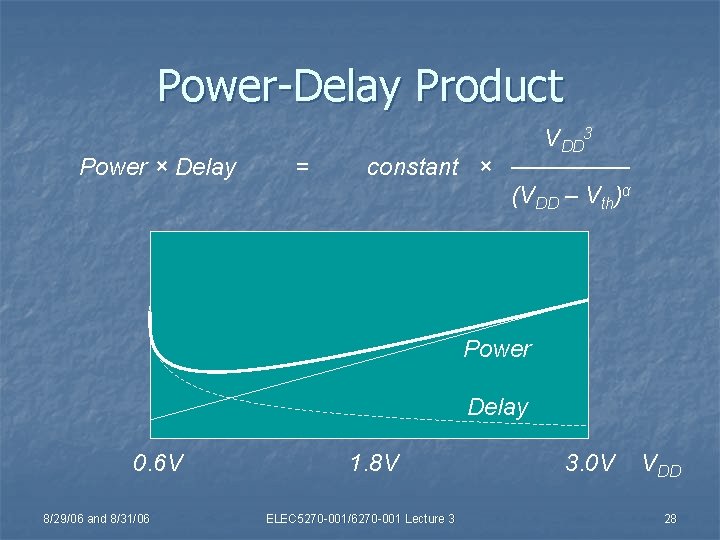
Power-Delay Product Power × Delay = VDD 3 constant × ─────── (VDD – Vth)α Power Delay 0. 6 V 8/29/06 and 8/31/06 1. 8 V ELEC 5270 -001/6270 -001 Lecture 3 3. 0 V VDD 28

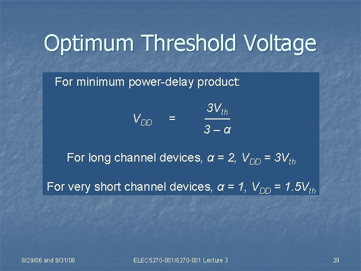
Optimum Threshold Voltage For minimum power-delay product: VDD = 3 Vth ─── 3–α For long channel devices, α = 2, VDD = 3 Vth For very short channel devices, α = 1, VDD = 1. 5 Vth 8/29/06 and 8/31/06 ELEC 5270 -001/6270 -001 Lecture 3 29

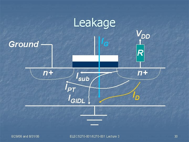
Leakage IG Ground R n+ Isub IPT IGIDL 8/29/06 and 8/31/06 VDD ELEC 5270 -001/6270 -001 Lecture 3 n+ ID 30

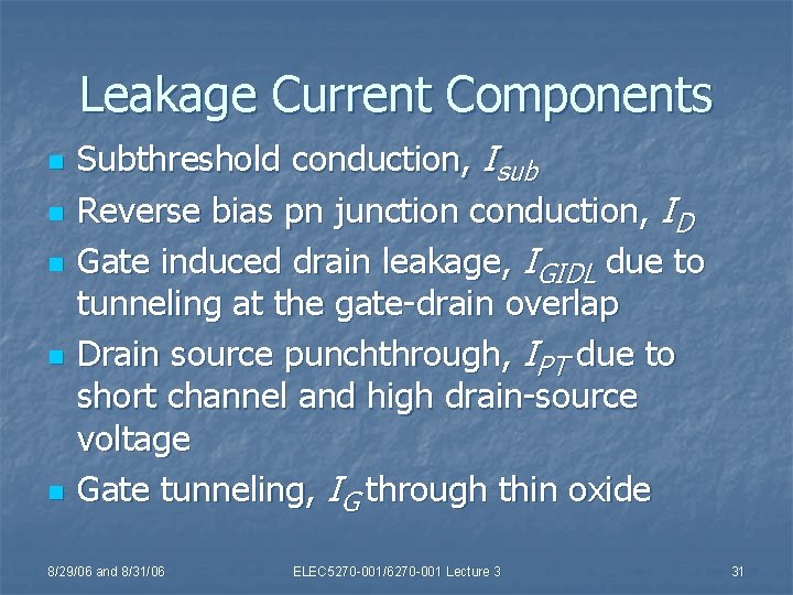
Leakage Current Components n n n Subthreshold conduction, Isub Reverse bias pn junction conduction, ID Gate induced drain leakage, IGIDL due to tunneling at the gate-drain overlap Drain source punchthrough, IPT due to short channel and high drain-source voltage Gate tunneling, IG through thin oxide 8/29/06 and 8/31/06 ELEC 5270 -001/6270 -001 Lecture 3 31

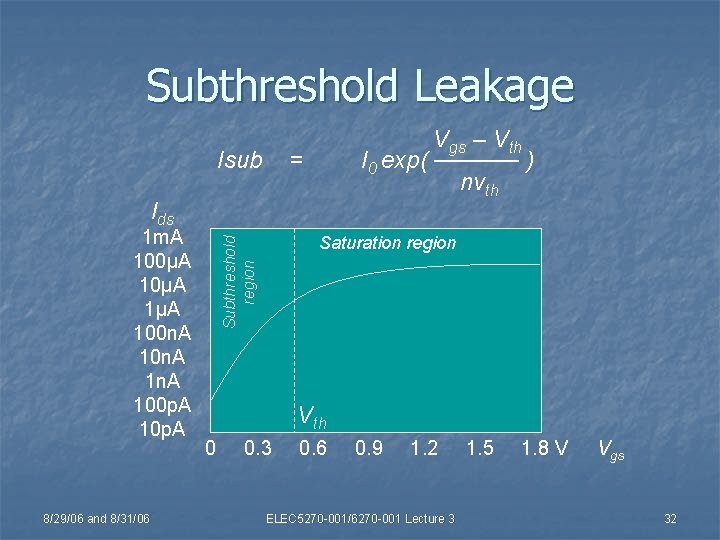
Subthreshold Leakage Isub Vgs – Vth I 0 exp( ───── ) nvth = Ids 8/29/06 and 8/31/06 Saturation region Subthreshold region 1 m. A 100μA 1μA 100 n. A 1 n. A 100 p. A 10 p. A Vth 0 0. 3 0. 6 0. 9 1. 2 ELEC 5270 -001/6270 -001 Lecture 3 1. 5 1. 8 V Vgs 32

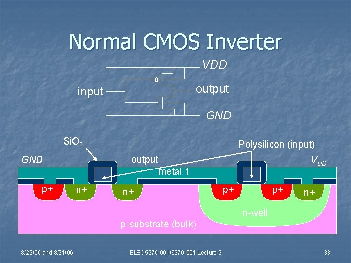
Normal CMOS Inverter VDD o input output GND Si. O 2 output metal 1 GND p+ Polysilicon (input) n+ n+ VDD p+ p+ n+ n-well p-substrate (bulk) 8/29/06 and 8/31/06 ELEC 5270 -001/6270 -001 Lecture 3 33

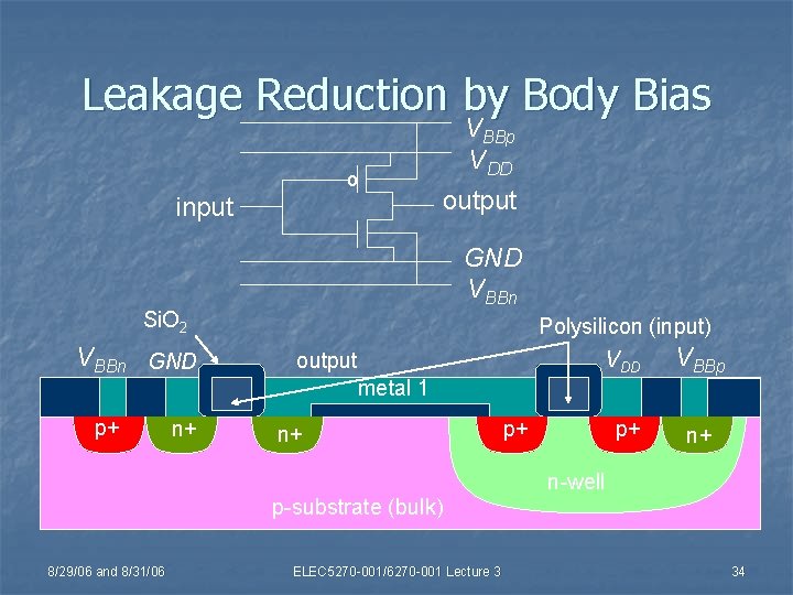
Leakage Reduction by Body Bias o input VBBp VDD output GND VBBn Si. O 2 VBBn GND p+ n+ Polysilicon (input) output metal 1 n+ VDD VBBp p+ n+ p+ n-well p-substrate (bulk) 8/29/06 and 8/31/06 ELEC 5270 -001/6270 -001 Lecture 3 34

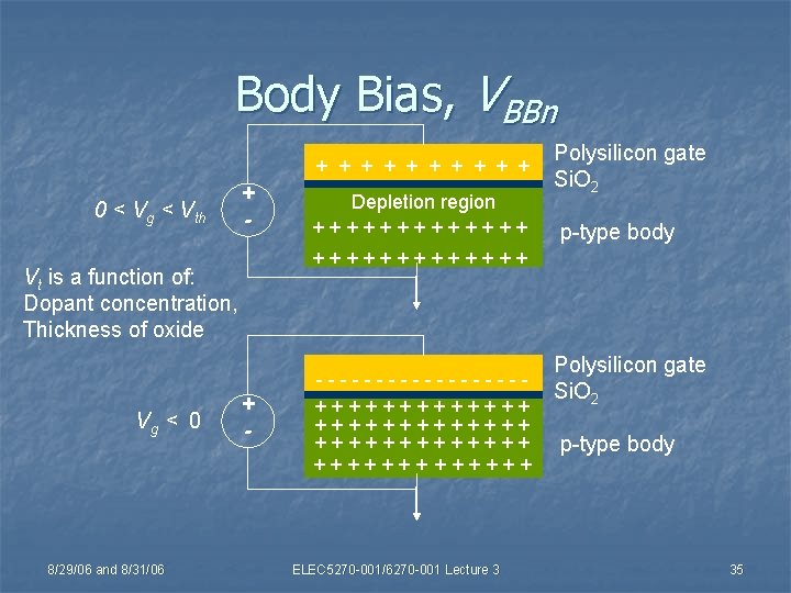
Body Bias, VBBn + + + + + 0 < Vg < Vth + - 8/29/06 and 8/31/06 p-type body +++++++ Vt is a function of: Dopant concentration, Thickness of oxide Vg < 0 Depletion region +++++++ Polysilicon gate Si. O 2 + - ---------+++++++++++++ ++++++ ELEC 5270 -001/6270 -001 Lecture 3 Polysilicon gate Si. O 2 p-type body 35

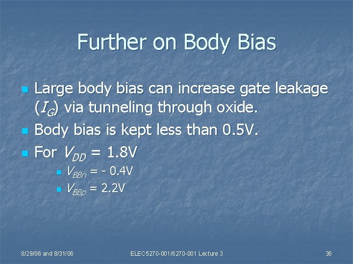
Further on Body Bias n n n Large body bias can increase gate leakage (IG) via tunneling through oxide. Body bias is kept less than 0. 5 V. For VDD = 1. 8 V VBBn = - 0. 4 V n VBBp = 2. 2 V n 8/29/06 and 8/31/06 ELEC 5270 -001/6270 -001 Lecture 3 36

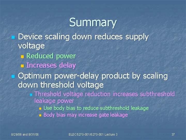
Summary n Device scaling down reduces supply voltage Reduced power n Increases delay n n Optimum power-delay product by scaling down threshold voltage n Threshold voltage reduction increases subthreshold leakage power n n 8/29/06 and 8/31/06 Use body bias to reduce subthreshold leakage Body bias may increase gate leakage ELEC 5270 -001/6270 -001 Lecture 3 37