ELEC 5200 0016200 001 Computer Architecture and Design




- Slides: 69

ELEC 5200 -001/6200 -001 Computer Architecture and Design Fall 2015 Memory Organization (Chapter 5) Vishwani D. Agrawal James J. Danaher Professor Department of Electrical and Computer Engineering Auburn University, Auburn, AL 36849 http: //www. eng. auburn. edu/~vagrawal@eng. auburn. edu Fall 2015, Nov 2. . . ELEC 5200 -001/6200 -001 Lecture 9 1

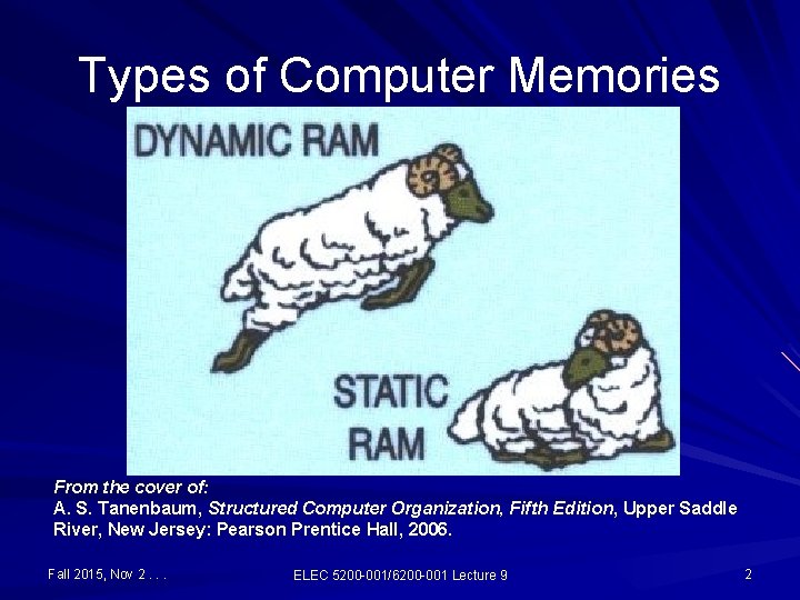
Types of Computer Memories From the cover of: A. S. Tanenbaum, Structured Computer Organization, Fifth Edition, Upper Saddle River, New Jersey: Pearson Prentice Hall, 2006. Fall 2015, Nov 2. . . ELEC 5200 -001/6200 -001 Lecture 9 2

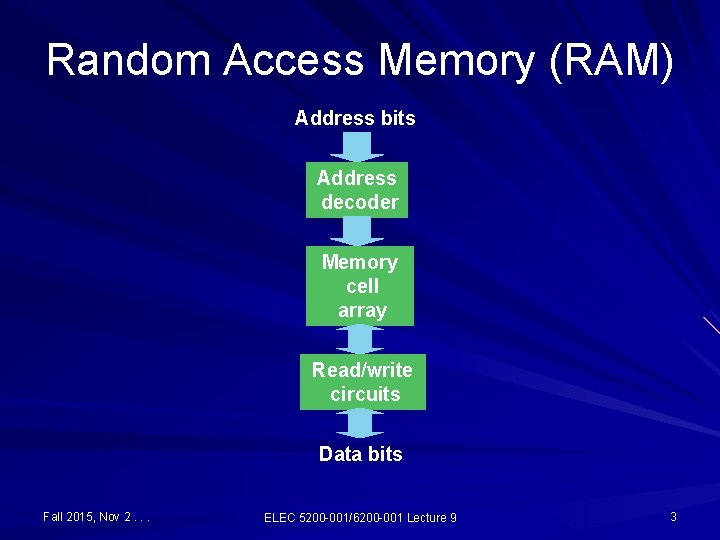
Random Access Memory (RAM) Address bits Address decoder Memory cell array Read/write circuits Data bits Fall 2015, Nov 2. . . ELEC 5200 -001/6200 -001 Lecture 9 3

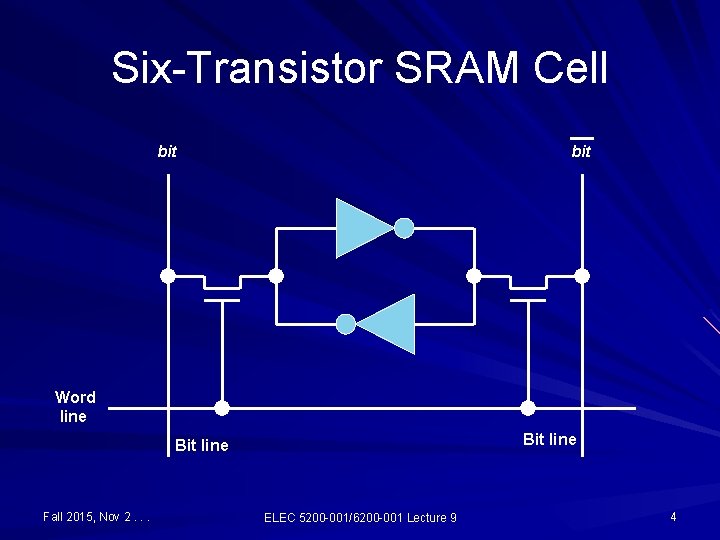
Six-Transistor SRAM Cell bit Word line Bit line Fall 2015, Nov 2. . . ELEC 5200 -001/6200 -001 Lecture 9 4

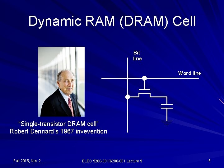
Dynamic RAM (DRAM) Cell Bit line Word line “Single-transistor DRAM cell” Robert Dennard’s 1967 invevention Fall 2015, Nov 2. . . ELEC 5200 -001/6200 -001 Lecture 9 5

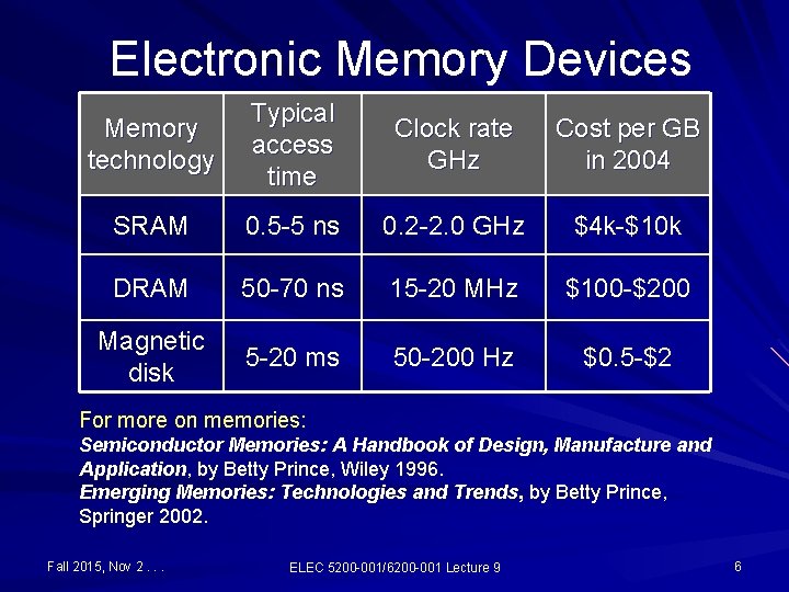
Electronic Memory Devices Memory technology Typical access time Clock rate GHz Cost per GB in 2004 SRAM 0. 5 -5 ns 0. 2 -2. 0 GHz $4 k-$10 k DRAM 50 -70 ns 15 -20 MHz $100 -$200 Magnetic disk 5 -20 ms 50 -200 Hz $0. 5 -$2 For more on memories: Semiconductor Memories: A Handbook of Design, Manufacture and Application, by Betty Prince, Wiley 1996. Emerging Memories: Technologies and Trends, by Betty Prince, Springer 2002. Fall 2015, Nov 2. . . ELEC 5200 -001/6200 -001 Lecture 9 6

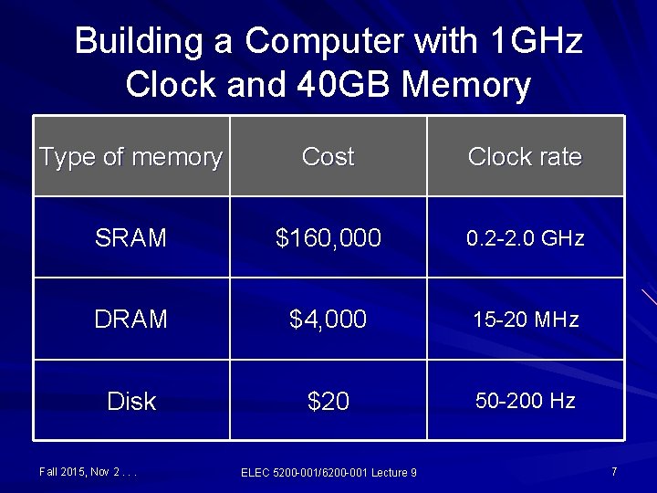
Building a Computer with 1 GHz Clock and 40 GB Memory Type of memory Cost Clock rate SRAM $160, 000 0. 2 -2. 0 GHz DRAM $4, 000 15 -20 MHz Disk $20 50 -200 Hz Fall 2015, Nov 2. . . ELEC 5200 -001/6200 -001 Lecture 9 7

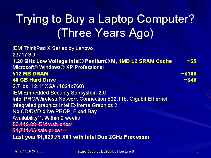
Trying to Buy a Laptop Computer? (Three Years Ago) IBM Think. Pad X Series by Lenovo 23717 GU 1. 20 GHz Low Voltage Intel® Pentium® M, 1 MB L 2 SRAM Cache Microsoft® Windows® XP Professional 512 MB DRAM 40 GB Hard Drive 2. 7 lbs, 12. 1" XGA (1024 x 768) IBM Embedded Security Subsystem 2. 0 Intel PRO/Wireless Network Connection 802. 11 b, Gigabit Ethernet Integrated graphics Intel Extreme Graphics 2 No CD/DVD drive PROP, Fixed Bay Availability**: Within 2 weeks $2, 149. 00 IBM web price* $1, 741. 65 sale price* Last year $1, 023. 75 X 61 with Intel Duo 2 GHz Processor Fall 2015, Nov 2. . . ELEC 5200 -001/6200 -001 Lecture 9 ~$5 ~$100 ~$40 8

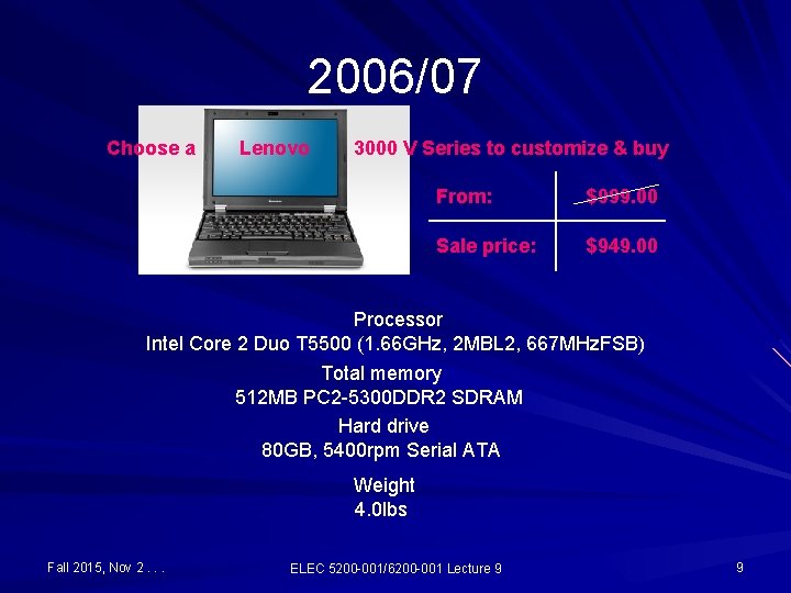
2006/07 Choose a Lenovo 3000 V Series to customize & buy From: $999. 00 Sale price: $949. 00 Processor Intel Core 2 Duo T 5500 (1. 66 GHz, 2 MBL 2, 667 MHz. FSB) Total memory 512 MB PC 2 -5300 DDR 2 SDRAM Hard drive 80 GB, 5400 rpm Serial ATA Weight 4. 0 lbs Fall 2015, Nov 2. . . ELEC 5200 -001/6200 -001 Lecture 9 9

2007 Executive-Class The classic, award-winning Think. Pad design remains unchanged - why mess with success? The Reserve Edition features a leather exterior handmade by expert Japanese saddle makers. Think. Pad Reserve Verizon Edition or Think. Pad Reserve Cingular Edition From $5, 000 Fall 2015, Nov 2. . . ELEC 5200 -001/6200 -001 Lecture 9 10

Nicholas Negroponte’s OLPC (One Laptop per Child) http: //www. flickr. com/photos/olpc/3145038187/ Fall 2015, Nov 2. . . ELEC 5200 -001/6200 -001 Lecture 9 11

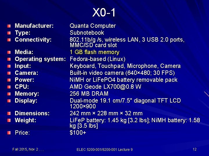
X 0 -1 Manufacturer: Type: Connectivity: Quanta Computer Subnotebook 802. 11 b/g /s, wireless LAN, 3 USB 2. 0 ports, MMC/SD card slot Media: 1 GB flash memory Operating system: Fedora-based (Linux) Input: Keyboard, Touchpad, Microphone, Camera: Built-in video camera (640× 480; 30 FPS) Power: Ni. MH or Li. Fe. PO 4 battery removable pack CPU: AMD Geode LX 700@0. 8 W Memory: 256 MB DRAM Display: Dual-mode 19. 1 cm/7. 5" diagonal TFT LCD 1200× 900 Dimensions: 242 mm × 228 mm × 32 mm Weight: Li. Fe. P battery: 1. 45 kg [3. 2 lbs]; Ni. MH battery: 1. 58 kg [3. 5 lbs] Price: $100+ Fall 2015, Nov 2. . . ELEC 5200 -001/6200 -001 Lecture 9 12

Today’s Laptop Inspiron 15 Dell Price $379. 99 Introducing the new Inspiron™ 15, a 15. 6" laptop that gives you the everyday features you need, all at a great value. Up to Intel® Core™ 2 Duo processors Entertainment on the go with the HD display Personalize with a choice of six vibrant colors or choose from over 200+ artist designs with Design Studio Fall 2015, Nov 2. . . ELEC 5200 -001/6200 -001 Lecture 9 13

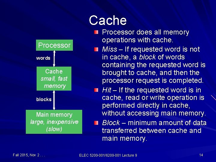
Cache Processor words Cache small, fast memory blocks Main memory large, inexpensive (slow) Fall 2015, Nov 2. . . Processor does all memory operations with cache. Miss – If requested word is not in cache, a block of words containing the requested word is brought to cache, and then the processor request is completed. Hit – If the requested word is in cache, read or write operation is performed directly in cache, without accessing main memory. Block – minimum amount of data transferred between cache and main memory. ELEC 5200 -001/6200 -001 Lecture 9 14

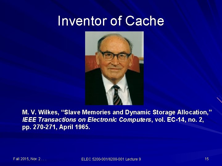
Inventor of Cache M. V. Wilkes, “Slave Memories and Dynamic Storage Allocation, ” IEEE Transactions on Electronic Computers, vol. EC-14, no. 2, pp. 270 -271, April 1965. Fall 2015, Nov 2. . . ELEC 5200 -001/6200 -001 Lecture 9 15

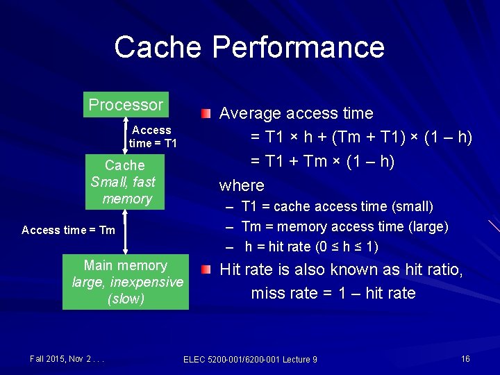
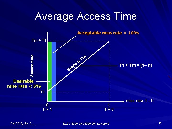
Cache Performance Processor Access time = T 1 Cache Small, fast memory Access time = Tm Main memory large, inexpensive (slow) Fall 2015, Nov 2. . . Average access time = T 1 × h + (Tm + T 1) × (1 – h) = T 1 + Tm × (1 – h) where – T 1 = cache access time (small) – Tm = memory access time (large) – h = hit rate (0 ≤ h ≤ 1) Hit rate is also known as hit ratio, miss rate = 1 – hit rate ELEC 5200 -001/6200 -001 Lecture 9 16

Average Access Time Acceptable miss rate < 10% Access time Tm + T 1 pe = Tm T 1 + Tm × (1– h) o Sl Desirable miss rate < 5% T 1 miss rate, 1 – h 0 h=1 Fall 2015, Nov 2. . . 1 h=0 ELEC 5200 -001/6200 -001 Lecture 9 17

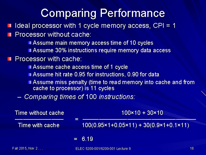
Comparing Performance Ideal processor with 1 cycle memory access, CPI = 1 Processor without cache: Assume main memory access time of 10 cycles Assume 30% instructions require memory data access Processor with cache: Assume cache access time of 1 cycle Assume hit rate 0. 95 for instructions, 0. 90 for data Assume miss penalty (time to read memory into cache and from cache to processor) is 11 cycles – Comparing times of 100 instructions: Time without cache 100× 10 + 30× 10 ────── = ────────────── Time with cache 100(0. 95× 1+0. 05× 11) + 30(0. 9× 1+0. 1× 11) = 6. 19 Fall 2015, Nov 2. . . ELEC 5200 -001/6200 -001 Lecture 9 18

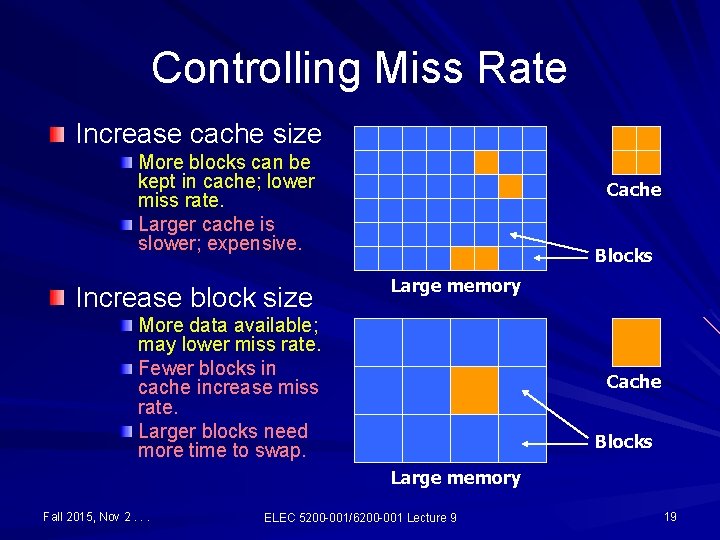
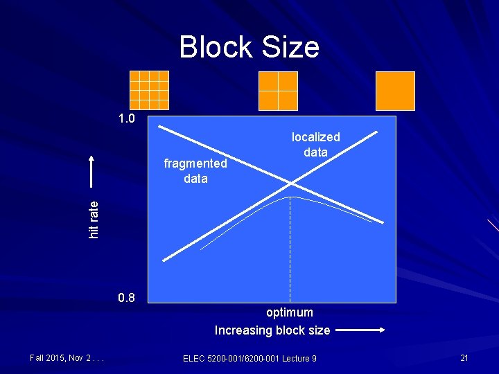
Controlling Miss Rate Increase cache size More blocks can be kept in cache; lower miss rate. Larger cache is slower; expensive. Increase block size Cache Blocks Large memory More data available; may lower miss rate. Fewer blocks in cache increase miss rate. Larger blocks need more time to swap. Cache Blocks Large memory Fall 2015, Nov 2. . . ELEC 5200 -001/6200 -001 Lecture 9 19

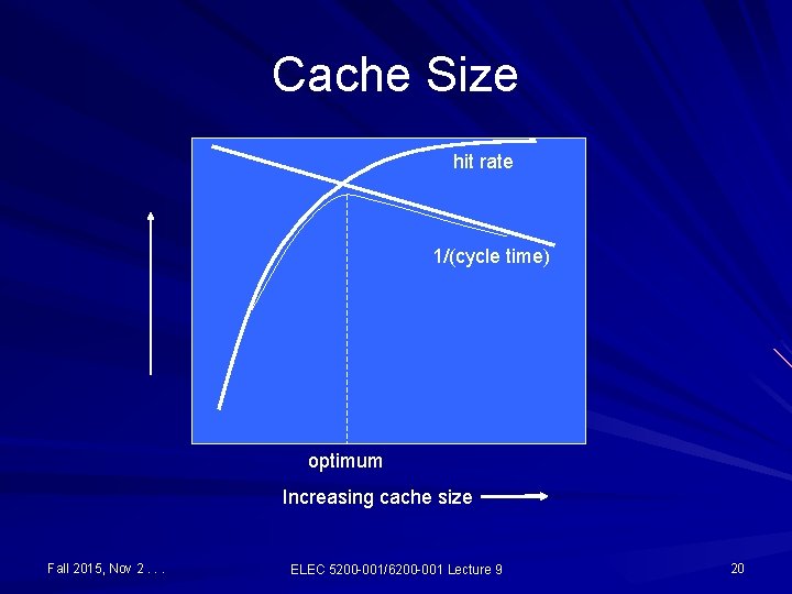
Cache Size hit rate 1/(cycle time) optimum Increasing cache size Fall 2015, Nov 2. . . ELEC 5200 -001/6200 -001 Lecture 9 20

Block Size 1. 0 hit rate fragmented data localized data 0. 8 optimum Increasing block size Fall 2015, Nov 2. . . ELEC 5200 -001/6200 -001 Lecture 9 21

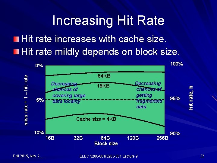
Increasing Hit Rate Hit rate increases with cache size. Hit rate mildly depends on block size. 100% 64 KB 5% Decreasing chances of covering large data locality 16 KB Decreasing chances of getting fragmented data 95% hit rate, h miss rate = 1 – hit rate 0% Cache size = 4 KB 10% 16 B Fall 2015, Nov 2. . . 32 B 64 B Block size 128 B ELEC 5200 -001/6200 -001 Lecture 9 256 B 90% 22

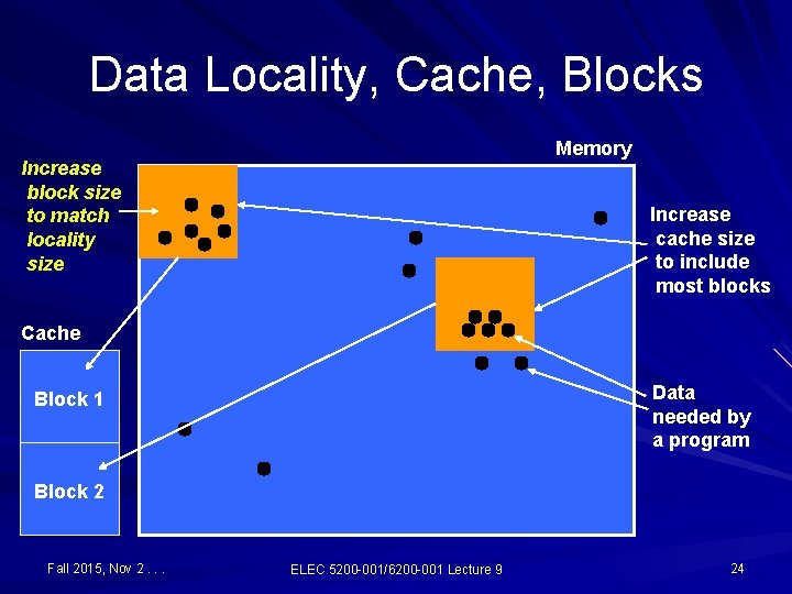
The Locality Principle A program tends to access data that form a physical cluster in the memory – multiple accesses may be made within the same block. Physical localities are temporal and may shift over longer periods of time – data not used for some time is less likely to be used in the future. Upon miss, the least recently used (LRU) block can be overwritten by a new block. P. J. Denning, “The Locality Principle, ” Communications of the ACM, vol. 48, no. 7, pp. 19 -24, July 2005. Fall 2015, Nov 2. . . ELEC 5200 -001/6200 -001 Lecture 9 23

Data Locality, Cache, Blocks Memory Increase block size to match locality size Increase cache size to include most blocks Cache Data needed by a program Block 1 Block 2 Fall 2015, Nov 2. . . ELEC 5200 -001/6200 -001 Lecture 9 24

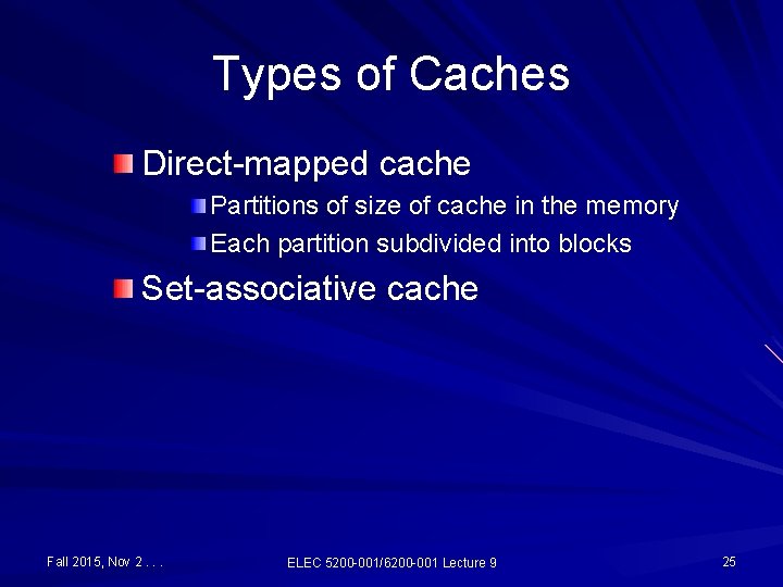
Types of Caches Direct-mapped cache Partitions of size of cache in the memory Each partition subdivided into blocks Set-associative cache Fall 2015, Nov 2. . . ELEC 5200 -001/6200 -001 Lecture 9 25

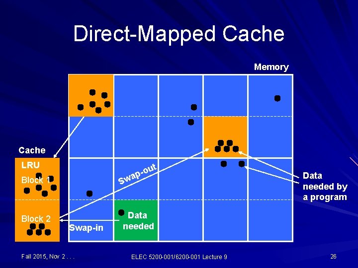
Direct-Mapped Cache Memory Cache LRU ou p a Sw Block 1 Block 2 t Swap-in Fall 2015, Nov 2. . . Data needed by a program Data needed ELEC 5200 -001/6200 -001 Lecture 9 26

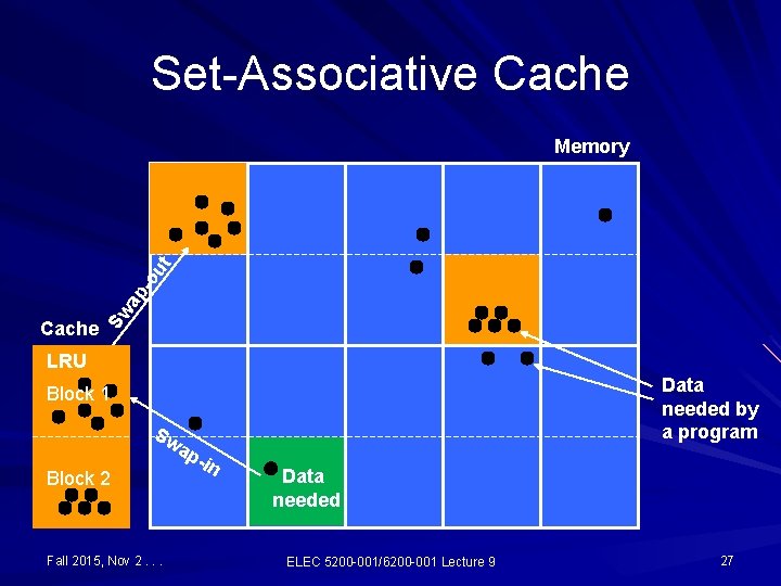
Set-Associative Cache Sw ap - ou t Memory LRU Data needed by a program Block 1 Sw ap Block 2 Fall 2015, Nov 2. . . -in Data needed ELEC 5200 -001/6200 -001 Lecture 9 27

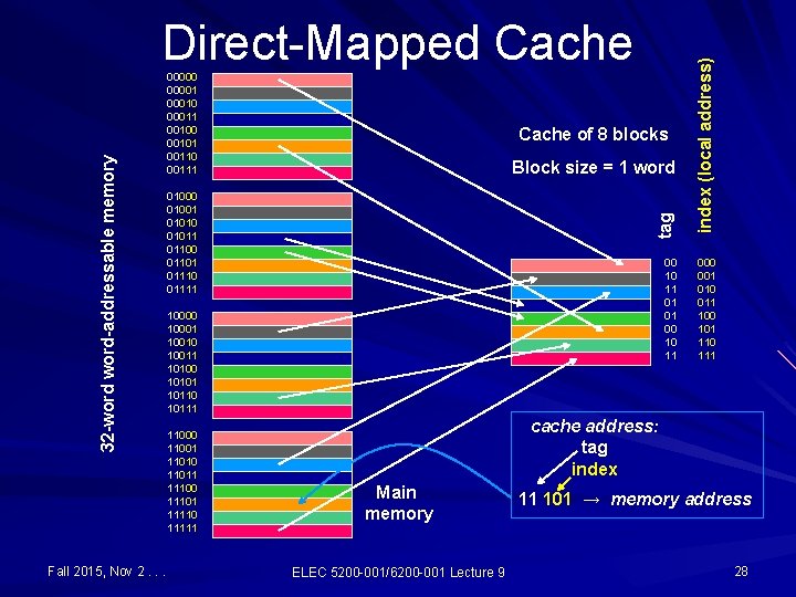
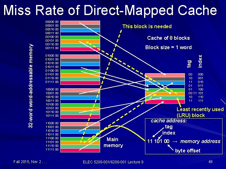
Fall 2015, Nov 2. . . Cache of 8 blocks Block size = 1 word 01000 01001 01010 01011 01100 01101 01110 01111 00 10 11 01 01 00 10 11 10000 10001 10010 10011 10100 10101 10110 10111 11000 11001 11010 11011 11100 11101 11110 11111 index (local address) 000001 00010 00011 00100 00101 00110 00111 tag 32 -word-addressable memory Direct-Mapped Cache 000 001 010 011 100 101 110 111 cache address: tag index Main memory ELEC 5200 -001/6200 -001 Lecture 9 11 101 → memory address 28

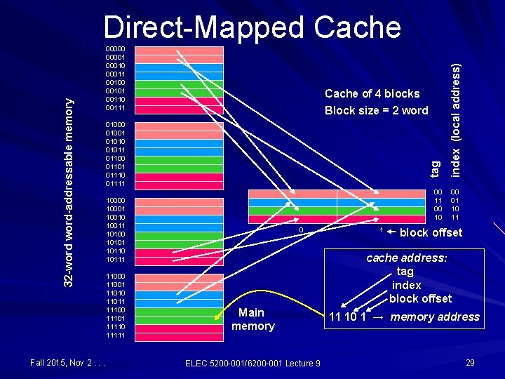
Fall 2015, Nov 2. . . Cache of 4 blocks Block size = 2 word 01000 01001 01010 01011 01100 01101 01110 01111 00 10 10001 10010 10011 10100 10101 10110 10111 11000 11001 11010 11011 11100 11101 11110 11111 0 1 index (local address) 000001 00010 00011 00100 00101 00110 00111 tag 32 -word-addressable memory Direct-Mapped Cache 00 01 10 11 block offset cache address: tag index block offset Main memory ELEC 5200 -001/6200 -001 Lecture 9 11 10 1 → memory address 29

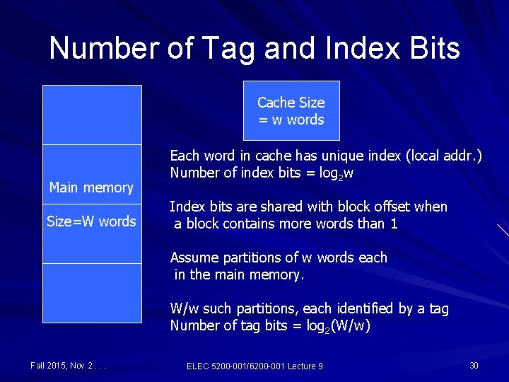
Number of Tag and Index Bits Cache Size = w words Main memory Size=W words Each word in cache has unique index (local addr. ) Number of index bits = log 2 w Index bits are shared with block offset when a block contains more words than 1 Assume partitions of w words each in the main memory. W/w such partitions, each identified by a tag Number of tag bits = log 2(W/w) Fall 2015, Nov 2. . . ELEC 5200 -001/6200 -001 Lecture 9 30

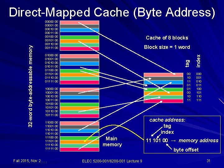
00000 00 00001 00 00010 00 00011 00 00100 00 00101 00 00110 00 00111 00 Cache of 8 blocks 01000 00 01001 00 01010 00 01011 00 01100 00 01101 00 01110 00 01111 00 index Block size = 1 word tag 32 -word byte-addressable memory Direct-Mapped Cache (Byte Address) 00 10 11 01 01 00 10 11 000 001 010 011 100 101 110 111 10000 00 10001 00 10010 00 10011 00 10100 00 10101 00 10110 00 10111 00 11000 00 11001 00 11010 00 11011 00 11100 00 11101 00 11110 00 11111 00 Fall 2015, Nov 2. . . cache address: tag index Main memory ELEC 5200 -001/6200 -001 Lecture 9 11 101 00 → memory address byte offset 31

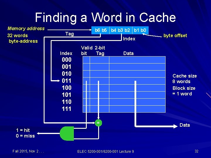
Finding a Word in Cache Memory address 32 words byte-address Tag Index b 6 b 5 b 4 b 3 b 2 b 1 b 0 Index Valid 2 -bit Tag byte offset Data 000 001 010 011 100 101 110 111 Cache size 8 words Block size = 1 word = Data 1 = hit 0 = miss Fall 2015, Nov 2. . . ELEC 5200 -001/6200 -001 Lecture 9 32

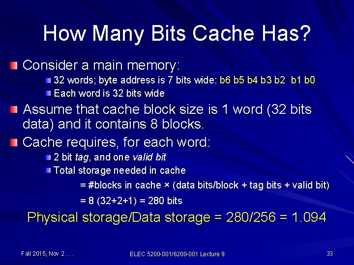
How Many Bits Cache Has? Consider a main memory: 32 words; byte address is 7 bits wide: b 6 b 5 b 4 b 3 b 2 b 1 b 0 Each word is 32 bits wide Assume that cache block size is 1 word (32 bits data) and it contains 8 blocks. Cache requires, for each word: 2 bit tag, and one valid bit Total storage needed in cache = #blocks in cache × (data bits/block + tag bits + valid bit) = 8 (32+2+1) = 280 bits Physical storage/Data storage = 280/256 = 1. 094 Fall 2015, Nov 2. . . ELEC 5200 -001/6200 -001 Lecture 9 33

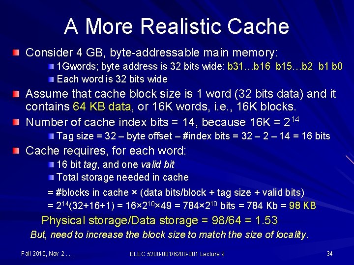
A More Realistic Cache Consider 4 GB, byte-addressable main memory: 1 Gwords; byte address is 32 bits wide: b 31…b 16 b 15…b 2 b 1 b 0 Each word is 32 bits wide Assume that cache block size is 1 word (32 bits data) and it contains 64 KB data, or 16 K words, i. e. , 16 K blocks. Number of cache index bits = 14, because 16 K = 214 Tag size = 32 – byte offset – #index bits = 32 – 14 = 16 bits Cache requires, for each word: 16 bit tag, and one valid bit Total storage needed in cache = #blocks in cache × (data bits/block + tag size + valid bits) = 214(32+16+1) = 16× 210× 49 = 784× 210 bits = 784 Kb = 98 KB Physical storage/Data storage = 98/64 = 1. 53 But, need to increase the block size to match the size of locality. Fall 2015, Nov 2. . . ELEC 5200 -001/6200 -001 Lecture 9 34

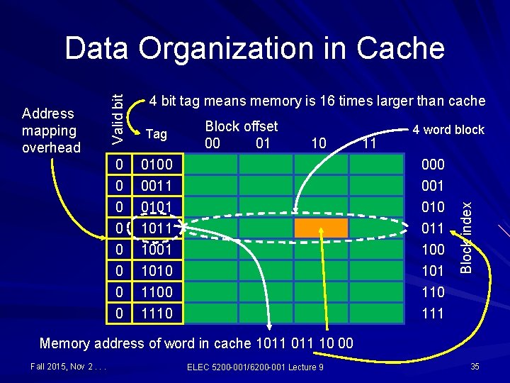
Data Organization in Cache Valid bit Tag 0 0 0100 0011 000 001 0 0 0 0101 1011 1001 1010 1100 1110 011 100 101 110 111 Block offset 00 01 10 11 4 word block Block index Address mapping overhead 4 bit tag means memory is 16 times larger than cache Memory address of word in cache 1011 10 00 Fall 2015, Nov 2. . . ELEC 5200 -001/6200 -001 Lecture 9 35

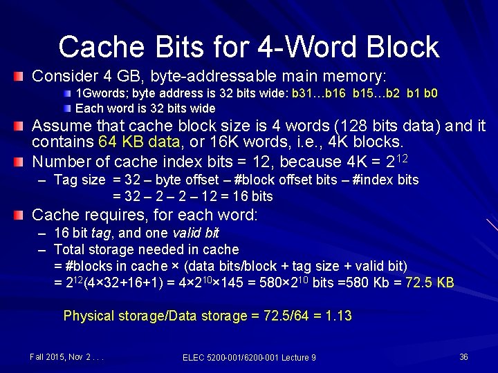
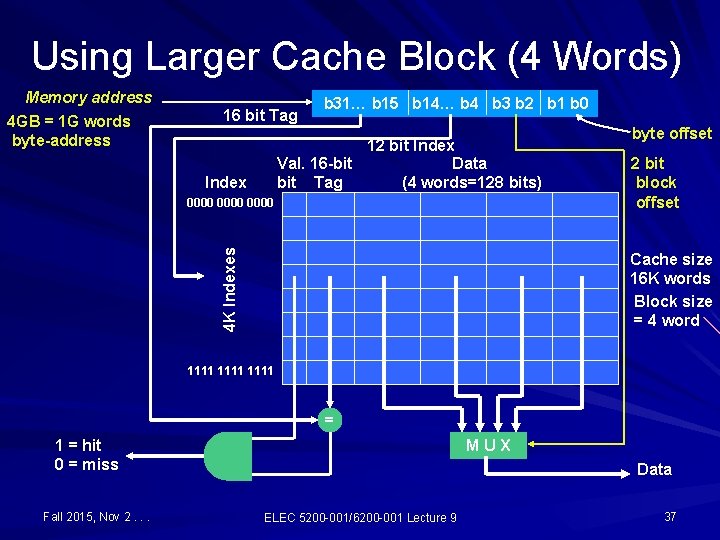
Cache Bits for 4 -Word Block Consider 4 GB, byte-addressable main memory: 1 Gwords; byte address is 32 bits wide: b 31…b 16 b 15…b 2 b 1 b 0 Each word is 32 bits wide Assume that cache block size is 4 words (128 bits data) and it contains 64 KB data, or 16 K words, i. e. , 4 K blocks. Number of cache index bits = 12, because 4 K = 212 – Tag size = 32 – byte offset – #block offset bits – #index bits = 32 – 2 – 12 = 16 bits Cache requires, for each word: – – 16 bit tag, and one valid bit Total storage needed in cache = #blocks in cache × (data bits/block + tag size + valid bit) = 212(4× 32+16+1) = 4× 210× 145 = 580× 210 bits =580 Kb = 72. 5 KB Physical storage/Data storage = 72. 5/64 = 1. 13 Fall 2015, Nov 2. . . ELEC 5200 -001/6200 -001 Lecture 9 36

Using Larger Cache Block (4 Words) Memory address 4 GB = 1 G words byte-address 16 bit Tag b 31… b 15 b 14… b 4 b 3 b 2 b 1 b 0 12 bit Index Val. 16 -bit Data bit Tag (4 words=128 bits) Index 4 K Indexes 0000 byte offset 2 bit block offset Cache size 16 K words Block size = 4 word 1111 = hit 0 = miss Fall 2015, Nov 2. . . MUX Data ELEC 5200 -001/6200 -001 Lecture 9 37

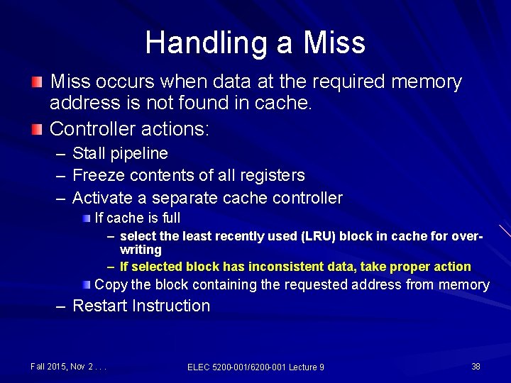
Handling a Miss occurs when data at the required memory address is not found in cache. Controller actions: – – – Stall pipeline Freeze contents of all registers Activate a separate cache controller If cache is full – select the least recently used (LRU) block in cache for overwriting – If selected block has inconsistent data, take proper action Copy the block containing the requested address from memory – Restart Instruction Fall 2015, Nov 2. . . ELEC 5200 -001/6200 -001 Lecture 9 38

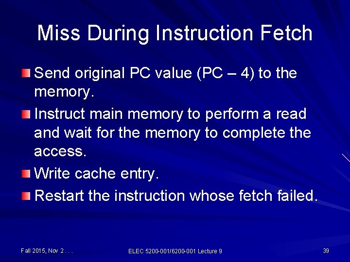
Miss During Instruction Fetch Send original PC value (PC – 4) to the memory. Instruct main memory to perform a read and wait for the memory to complete the access. Write cache entry. Restart the instruction whose fetch failed. Fall 2015, Nov 2. . . ELEC 5200 -001/6200 -001 Lecture 9 39

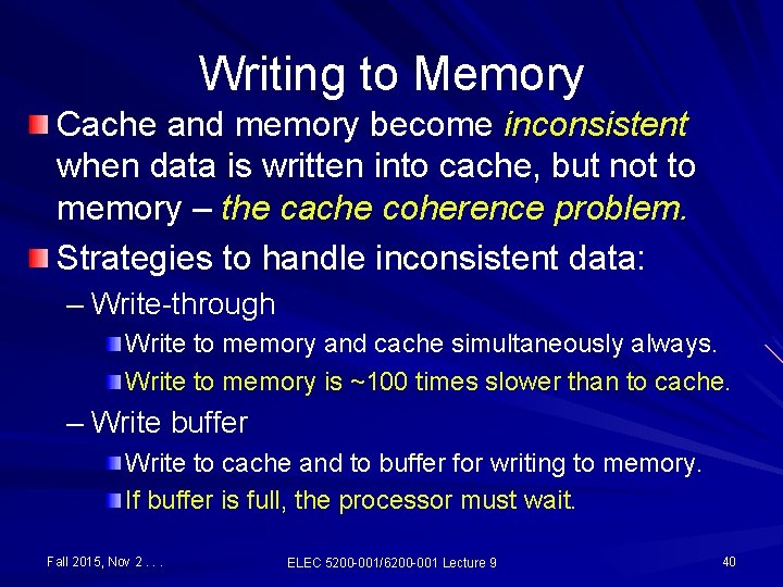
Writing to Memory Cache and memory become inconsistent when data is written into cache, but not to memory – the cache coherence problem. Strategies to handle inconsistent data: – Write-through Write to memory and cache simultaneously always. Write to memory is ~100 times slower than to cache. – Write buffer Write to cache and to buffer for writing to memory. If buffer is full, the processor must wait. Fall 2015, Nov 2. . . ELEC 5200 -001/6200 -001 Lecture 9 40

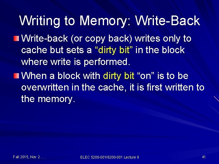
Writing to Memory: Write-Back Write-back (or copy back) writes only to cache but sets a “dirty bit” in the block where write is performed. When a block with dirty bit “on” is to be overwritten in the cache, it is first written to the memory. Fall 2015, Nov 2. . . ELEC 5200 -001/6200 -001 Lecture 9 41

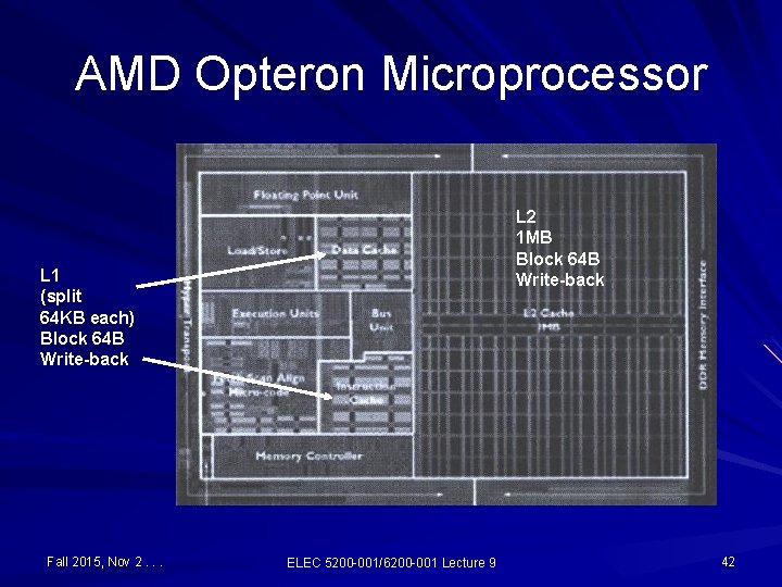
AMD Opteron Microprocessor L 2 1 MB Block 64 B Write-back L 1 (split 64 KB each) Block 64 B Write-back Fall 2015, Nov 2. . . ELEC 5200 -001/6200 -001 Lecture 9 42

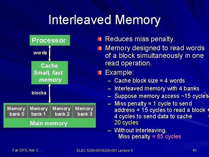
Interleaved Memory Reduces miss penalty. Memory designed to read words of a block simultaneously in one read operation. Example: Processor words Cache Small, fast memory blocks Memory bank 0 Memory bank 1 Memory bank 2 Main memory Fall 2015, Nov 2. . . Memory bank 3 – – Cache block size = 4 words Interleaved memory with 4 banks Suppose memory access ~15 cycles Miss penalty = 1 cycle to send address + 15 cycles to read a block + 4 cycles to send data to cache = 20 cycles – Without interleaving, Miss penalty = 65 cycles ELEC 5200 -001/6200 -001 Lecture 9 43

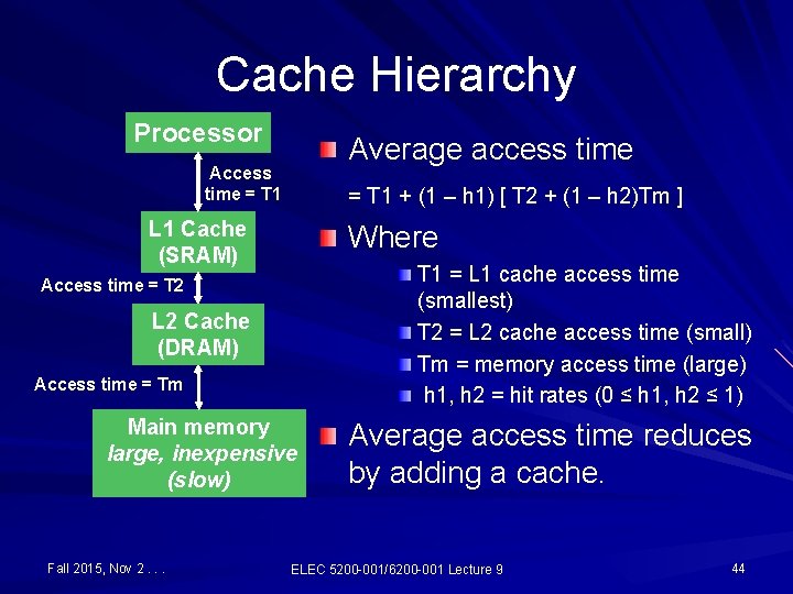
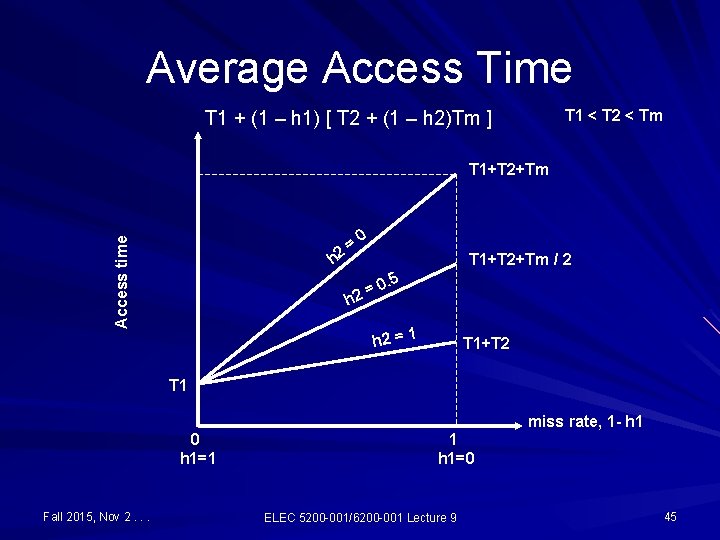
Cache Hierarchy Processor Average access time Access time = T 1 + (1 – h 1) [ T 2 + (1 – h 2)Tm ] L 1 Cache (SRAM) Where T 1 = L 1 cache access time (smallest) T 2 = L 2 cache access time (small) Tm = memory access time (large) h 1, h 2 = hit rates (0 ≤ h 1, h 2 ≤ 1) Access time = T 2 L 2 Cache (DRAM) Access time = Tm Main memory large, inexpensive (slow) Fall 2015, Nov 2. . . Average access time reduces by adding a cache. ELEC 5200 -001/6200 -001 Lecture 9 44

Average Access Time T 1 < T 2 < Tm T 1 + (1 – h 1) [ T 2 + (1 – h 2)Tm ] Access time T 1+T 2+Tm h 2 = 0 T 1+T 2+Tm / 2 . 5 0 2= h h 2 = 1 T 1+T 2 T 1 miss rate, 1 - h 1 0 h 1=1 Fall 2015, Nov 2. . . 1 h 1=0 ELEC 5200 -001/6200 -001 Lecture 9 45

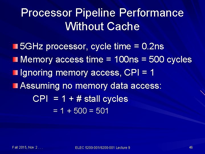
Processor Pipeline Performance Without Cache 5 GHz processor, cycle time = 0. 2 ns Memory access time = 100 ns = 500 cycles Ignoring memory access, CPI = 1 Assuming no memory data access: CPI = 1 + # stall cycles = 1 + 500 = 501 Fall 2015, Nov 2. . . ELEC 5200 -001/6200 -001 Lecture 9 46

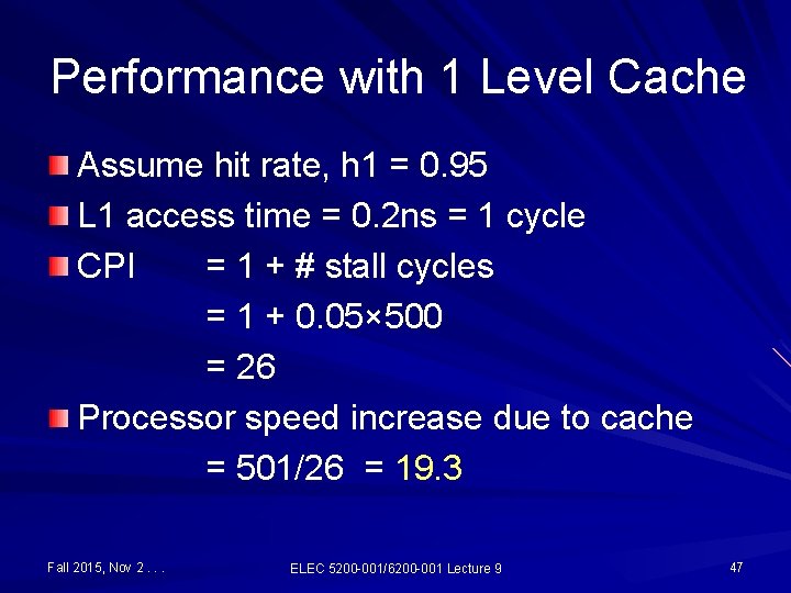
Performance with 1 Level Cache Assume hit rate, h 1 = 0. 95 L 1 access time = 0. 2 ns = 1 cycle CPI = 1 + # stall cycles = 1 + 0. 05× 500 = 26 Processor speed increase due to cache = 501/26 = 19. 3 Fall 2015, Nov 2. . . ELEC 5200 -001/6200 -001 Lecture 9 47

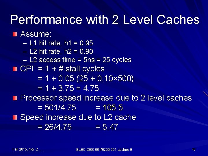
Performance with 2 Level Caches Assume: – L 1 hit rate, h 1 = 0. 95 – L 2 hit rate, h 2 = 0. 90 – L 2 access time = 5 ns = 25 cycles CPI = 1 + # stall cycles = 1 + 0. 05 (25 + 0. 10× 500) = 1 + 3. 75 = 4. 75 Processor speed increase due to 2 level caches = 501/4. 75 = 105. 5 Speed increase due to L 2 cache = 26/4. 75 = 5. 47 Fall 2015, Nov 2. . . ELEC 5200 -001/6200 -001 Lecture 9 48

This block is needed Cache of 8 blocks Block size = 1 word 01000 00 01001 00 01010 00 01011 00 01100 00 01101 00 01110 00 01111 00 00 10 11 01 01 00 11 10000 00 10001 00 10010 00 10011 00 10100 00 10101 00 10110 00 10111 00 11000 00 11001 00 11010 00 11011 00 11100 00 11101 00 11110 00 11111 00 Fall 2015, Nov 2. . . index 00000 00 00001 00 00010 00 00011 00 00100 00 00101 00 00110 00 00111 00 tag 32 -word-addressable memory Miss Rate of Direct-Mapped Cache 000 001 010 011 100 101 110 111 Least recently used (LRU) block cache address: tag index Main memory ELEC 5200 -001/6200 -001 Lecture 9 11 101 00 → memory address byte offset 49

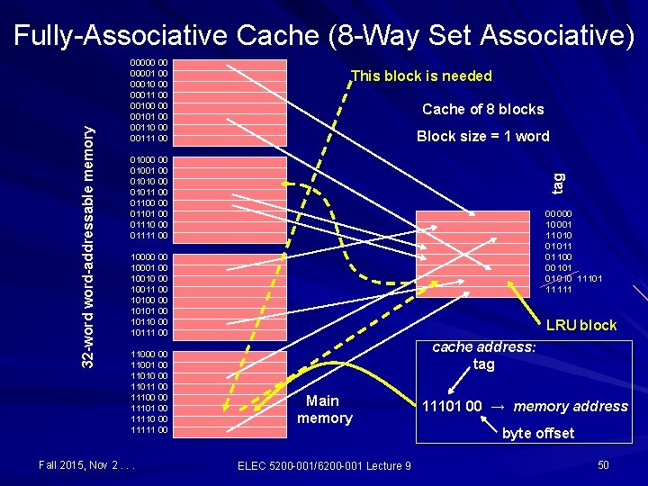
00000 00 00001 00 00010 00 00011 00 00100 00 00101 00 00110 00 00111 00 This block is needed Cache of 8 blocks Block size = 1 word 01000 00 01001 00 01010 00 01011 00 01100 00 01101 00 01110 00 01111 00 tag 32 -word-addressable memory Fully-Associative Cache (8 -Way Set Associative) 00 000 10 001 11 010 01 01 100 00 101 01 010 11101 11 10000 00 10001 00 10010 00 10011 00 10100 00 10101 00 10110 00 10111 00 11000 00 11001 00 11010 00 11011 00 11100 00 11101 00 11110 00 11111 00 Fall 2015, Nov 2. . . LRU block cache address: tag Main memory ELEC 5200 -001/6200 -001 Lecture 9 11101 00 → memory address byte offset 50

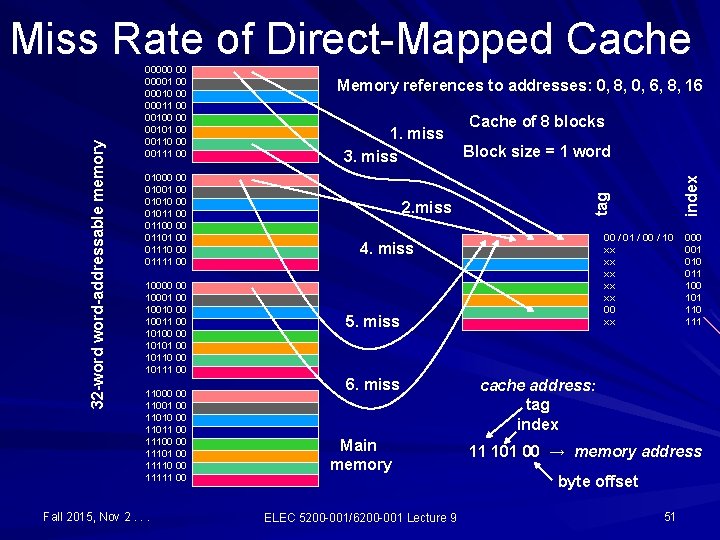
01000 00 01001 00 01010 00 01011 00 01100 00 01101 00 01110 00 01111 00 10000 00 10001 00 10010 00 10011 00 10100 00 10101 00 10110 00 10111 00 11000 00 11001 00 11010 00 11011 00 11100 00 11101 00 11110 00 11111 00 Fall 2015, Nov 2. . . Memory references to addresses: 0, 8, 0, 6, 8, 16 1. miss 3. miss 2. miss Cache of 8 blocks Block size = 1 word 00 / 01 / 00 / 10 xx xx xx 00 xx 4. miss 5. miss 6. miss Main memory ELEC 5200 -001/6200 -001 Lecture 9 index 00000 00 00001 00 00010 00 00011 00 00100 00 00101 00 00110 00 00111 00 tag 32 -word-addressable memory Miss Rate of Direct-Mapped Cache 000 001 010 011 100 101 110 111 cache address: tag index 11 101 00 → memory address byte offset 51

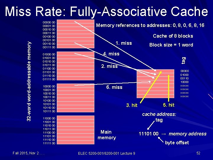
00000 00 00001 00 00010 00 00011 00 00100 00 00101 00 00110 00 00111 00 01000 00 01001 00 01010 00 01011 00 01100 00 01101 00 01110 00 01111 00 10000 00 10001 00 10010 00 10011 00 10100 00 10101 00 10110 00 10111 00 11000 00 11001 00 11010 00 11011 00 11100 00 11101 00 11110 00 11111 00 Fall 2015, Nov 2. . . Memory references to addresses: 0, 8, 0, 6, 8, 16 Cache of 8 blocks 1. miss Block size = 1 word 4. miss tag 32 -word-addressable memory Miss Rate: Fully-Associative Cache 2. miss 00000 01000 00110 10000 xxxxx 6. miss 3. hit 5. hit cache address: tag Main memory ELEC 5200 -001/6200 -001 Lecture 9 11101 00 → memory address byte offset 52

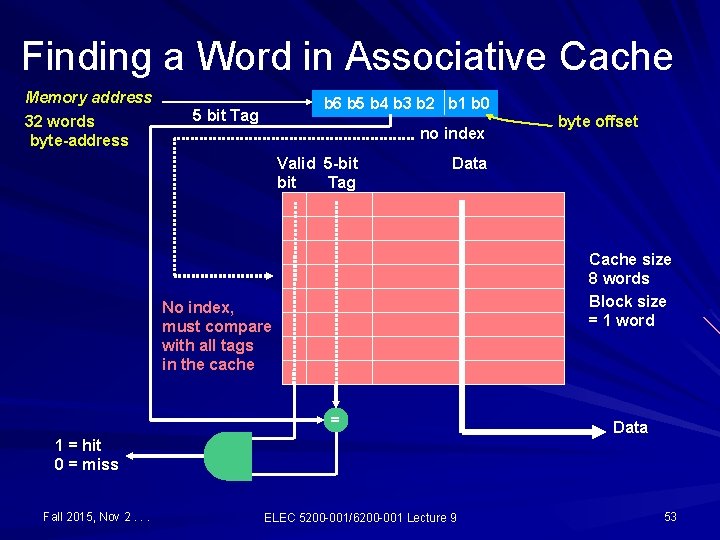
Finding a Word in Associative Cache Memory address 32 words byte-address b 6 b 5 b 4 b 3 b 2 b 1 b 0 5 bit Tag no index Valid 5 -bit Tag byte offset Data Cache size 8 words Block size = 1 word No index, must compare with all tags in the cache = Data 1 = hit 0 = miss Fall 2015, Nov 2. . . ELEC 5200 -001/6200 -001 Lecture 9 53

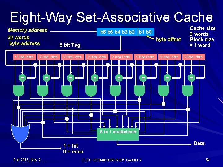
Eight-Way Set-Associative Cache Memory address 32 words byte-address V | tag | data = b 6 b 5 b 4 b 3 b 2 b 1 b 0 byte offset 5 bit Tag V | tag | data = = V | tag | data = Cache size 8 words Block size = 1 word V | tag | data = 8 to 1 multiplexer 1 = hit 0 = miss Fall 2015, Nov 2. . . ELEC 5200 -001/6200 -001 Lecture 9 Data 54

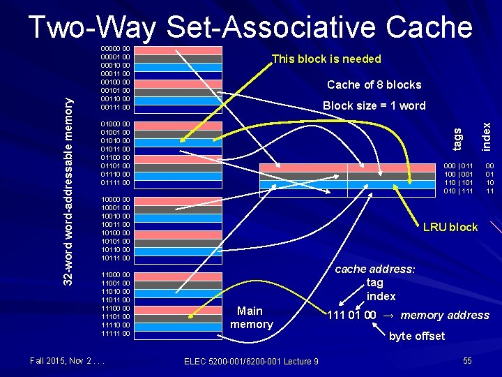
This block is needed Cache of 8 blocks Block size = 1 word 01000 00 01001 00 01010 00 01011 00 01100 00 01101 00 01110 00 01111 00 000 | 011 100 | 001 110 | 101 010 | 111 10000 00 10001 00 10010 00 10011 00 10100 00 10101 00 10110 00 10111 00 11000 00 11001 00 11010 00 11011 00 11100 00 11101 00 11110 00 11111 00 Fall 2015, Nov 2. . . index 00000 00 00001 00 00010 00 00011 00 00100 00 00101 00 00110 00 00111 00 tags 32 -word-addressable memory Two-Way Set-Associative Cache 00 01 10 11 LRU block cache address: tag index Main memory ELEC 5200 -001/6200 -001 Lecture 9 111 01 00 → memory address byte offset 55

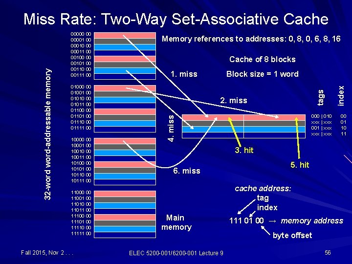
10000 00 10001 00 10010 00 10011 00 10100 00 10101 00 10110 00 10111 00 11000 00 11001 00 11010 00 11011 00 11100 00 11101 00 11110 00 11111 00 Fall 2015, Nov 2. . . Cache of 8 blocks 1. miss Block size = 1 word 2. miss 000 | 010 xxx | xxx 001 | xxx index 01000 00 01001 00 01010 00 01011 00 01100 00 01101 00 01110 00 01111 00 Memory references to addresses: 0, 8, 0, 6, 8, 16 tags 00000 00 00001 00 00010 00 00011 00 00100 00 00101 00 00110 00 00111 00 4. miss 32 -word-addressable memory Miss Rate: Two-Way Set-Associative Cache 00 01 10 11 3. hit 6. miss 5. hit cache address: tag index Main memory ELEC 5200 -001/6200 -001 Lecture 9 111 01 00 → memory address byte offset 56

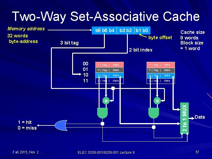
Two-Way Set-Associative Cache Memory address 32 words byte-address b 6 b 5 b 4 b 3 b 2 b 1 b 0 byte offset 3 bit tag 2 bit index 00 01 10 11 V | tag | data V | tag | data 1 = hit 0 = miss Fall 2015, Nov 2. . . = 2 to 1 MUX = Cache size 8 words Block size = 1 word ELEC 5200 -001/6200 -001 Lecture 9 Data 57

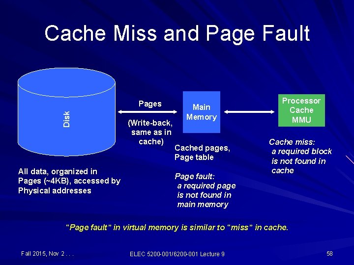
Cache Miss and Page Fault Disk Pages All data, organized in Pages (~4 KB), accessed by Physical addresses (Write-back, same as in cache) Main Memory Processor Cache MMU Cached pages, Page table Cache miss: a required block is not found in cache Page fault: a required page is not found in main memory “Page fault” in virtual memory is similar to “miss” in cache. Fall 2015, Nov 2. . . ELEC 5200 -001/6200 -001 Lecture 9 58

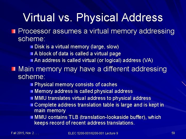
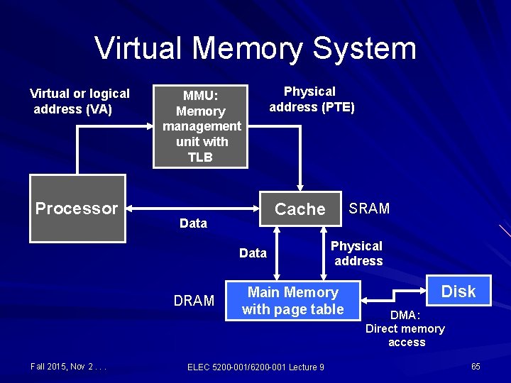
Virtual vs. Physical Address Processor assumes a virtual memory addressing scheme: Disk is a virtual memory (large, slow) A block of data is called a virtual page An address is called virtual (or logical) address (VA) Main memory may have a different addressing scheme: Physical memory consists of caches Memory address is called physical address MMU translates virtual address to physical address Complete address translation table is large and is kept in main memory MMU contains TLB (translation-lookaside buffer), which keeps record of recent address translations. Fall 2015, Nov 2. . . ELEC 5200 -001/6200 -001 Lecture 9 59

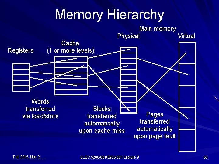
Memory Hierarchy Main memory Physical Virtual Cache Registers (1 or more levels) Words transferred via load/store Fall 2015, Nov 2. . . Blocks transferred automatically upon cache miss Pages transferred automatically upon page fault ELEC 5200 -001/6200 -001 Lecture 9 60

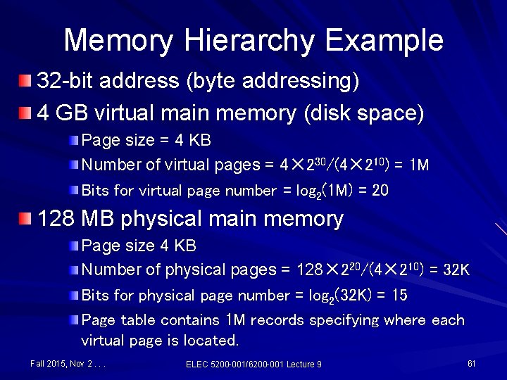
Memory Hierarchy Example 32 -bit address (byte addressing) 4 GB virtual main memory (disk space) Page size = 4 KB Number of virtual pages = 4✕ 230/(4✕ 210) = 1 M Bits for virtual page number = log 2(1 M) = 20 128 MB physical main memory Page size 4 KB Number of physical pages = 128✕ 220/(4✕ 210) = 32 K Bits for physical page number = log 2(32 K) = 15 Page table contains 1 M records specifying where each virtual page is located. Fall 2015, Nov 2. . . ELEC 5200 -001/6200 -001 Lecture 9 61

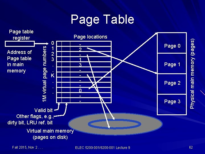
Page table register 1 M virtual page numbers Address of Page table in main memory Page locations 0 1 2 3. . K. . . 2 1 3 0 - Valid bit Other flags, e. g. , dirty bit, LRU ref. bit Page 0 Page 1 Page 2 Page 3 Physical main memory (pages) Page Table Virtual main memory (pages on disk) Fall 2015, Nov 2. . . ELEC 5200 -001/6200 -001 Lecture 9 62

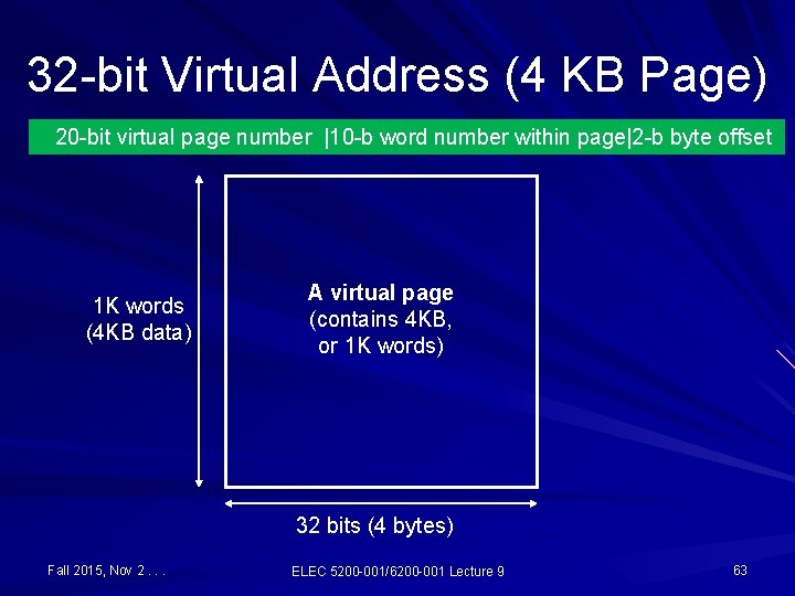
32 -bit Virtual Address (4 KB Page) 20 -bit virtual page number |10 -b word number within page|2 -b byte offset 1 K words (4 KB data) A virtual page (contains 4 KB, or 1 K words) 32 bits (4 bytes) Fall 2015, Nov 2. . . ELEC 5200 -001/6200 -001 Lecture 9 63

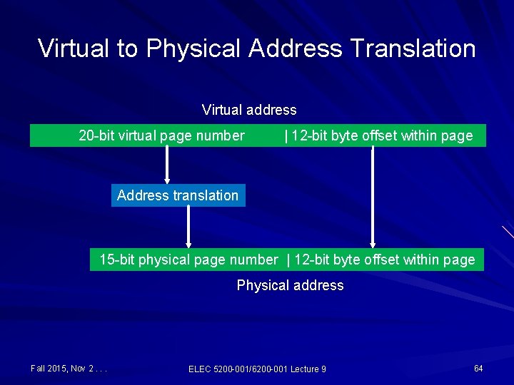
Virtual to Physical Address Translation Virtual address 20 -bit virtual page number | 12 -bit byte offset within page Address translation 15 -bit physical page number | 12 -bit byte offset within page Physical address Fall 2015, Nov 2. . . ELEC 5200 -001/6200 -001 Lecture 9 64

Virtual Memory System Virtual or logical address (VA) Processor Physical address (PTE) MMU: Memory management unit with TLB Cache Data DRAM Fall 2015, Nov 2. . . SRAM Physical address Main Memory with page table ELEC 5200 -001/6200 -001 Lecture 9 Disk DMA: Direct memory access 65

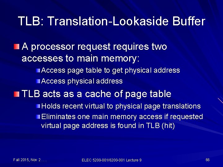
TLB: Translation-Lookaside Buffer A processor request requires two accesses to main memory: Access page table to get physical address Access physical address TLB acts as a cache of page table Holds recent virtual to physical page translations Eliminates one main memory access if requested virtual page address is found in TLB (hit) Fall 2015, Nov 2. . . ELEC 5200 -001/6200 -001 Lecture 9 66

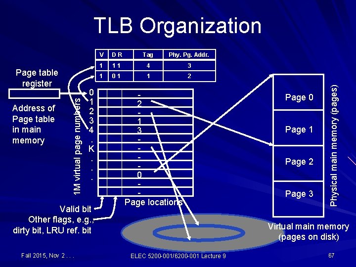
Address of Page table in main memory 1 M virtual page numbers Page table register 0 1 2 3 4. K. . . Valid bit Other flags, e. g. , dirty bit, LRU ref. bit Fall 2015, Nov 2. . . V DR Tag Phy. Pg. Addr. 1 11 4 3 1 01 1 2 2 1 3 0 Page locations Page 0 Page 1 Page 2 Page 3 Physical main memory (pages) TLB Organization Virtual main memory (pages on disk) ELEC 5200 -001/6200 -001 Lecture 9 67

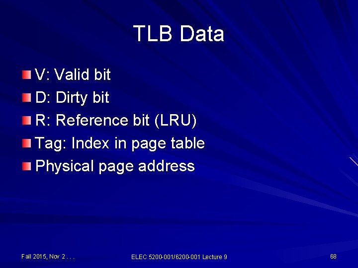
TLB Data V: Valid bit D: Dirty bit R: Reference bit (LRU) Tag: Index in page table Physical page address Fall 2015, Nov 2. . . ELEC 5200 -001/6200 -001 Lecture 9 68

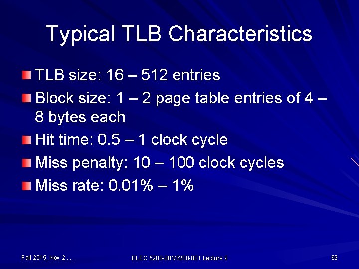
Typical TLB Characteristics TLB size: 16 – 512 entries Block size: 1 – 2 page table entries of 4 – 8 bytes each Hit time: 0. 5 – 1 clock cycle Miss penalty: 10 – 100 clock cycles Miss rate: 0. 01% – 1% Fall 2015, Nov 2. . . ELEC 5200 -001/6200 -001 Lecture 9 69