ELEC 516 VLSI System Design and Design Automation

- Slides: 61

ELEC 516 VLSI System Design and Design Automation Spring 2010 Lecture 5: Flip-Flop/Latch Design Reading Assignment: Rabaey: Chapter 7 Note: some of the figures in this slide set are adapted from the slide set of “ Digital Integrated Circuits” by Rabaey et. al. , Copyright 2002 1 ELEC 516/10 Lecture 5

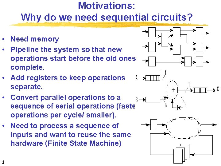
Motivations: Why do we need sequential circuits? • Need memory • Pipeline the system so that new operations start before the old ones complete. • Add registers to keep operations separate. • Convert parallel operations to a sequence of serial operations (faster operations per cycle/ smaller). • Need to process a sequence of inputs and want to reuse the same hardware (Finite State Machine) 2 ELEC 516/10 Lecture 5

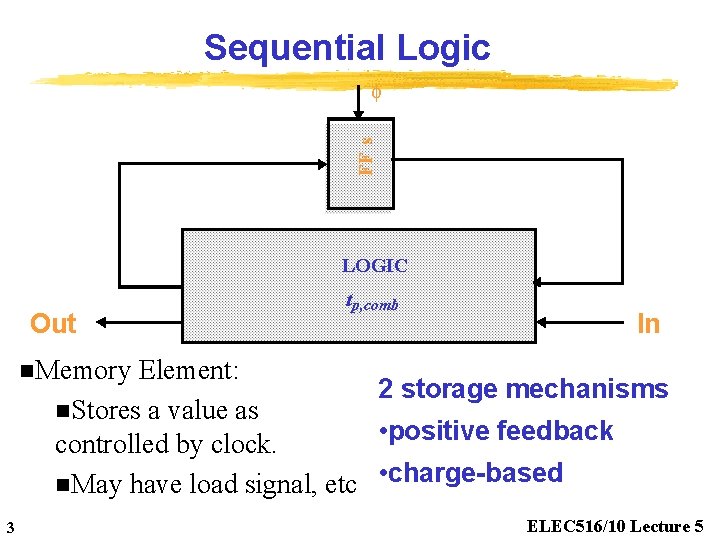
Sequential Logic FF s f LOGIC Out tp, comb In n. Memory Element: 2 storage mechanisms n. Stores a value as • positive feedback controlled by clock. n. May have load signal, etc • charge-based 3 ELEC 516/10 Lecture 5

Memory Elements - Latches and flip-flops • A generic memory element has an internal memory and some circuitry to control access to the internal memory. which is controlled by the clock input. • Memory element differ in many key respect: – exactly what form of clock signal causes the input data value to be read; – how the behavior of data around the read signal from clock affects the stored value; – when the stored value is presented to the output; – whethere is a combinational path from the input to the output. • 2 types of memory: latches and edge-triggered flip flop 4 – latches - transparent while the internal memory is being set from the data input – edge-triggered flip-flops (or register) - not transparent, reading the input value and changing the flip-flop’s output are two separate events. ELEC 516/10 Lecture 5

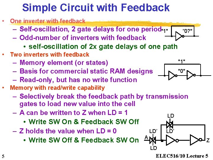
Simple Circuit with Feedback • One inverter with feedback – Self-oscillation, 2 gate delays for one period"1" – Odd-number of inverters with feedback • self-oscillation of 2 x gate delays of one path “ 0? " • Two inverters with feedback – Memory element (or states) – Basis for commercial static RAM designs – Read-only, but has no write function "1" "0" • Memory with read/write capability – Selectively break the feedback path by transmission gates to load new value into the cell – A can be written to Z when LD = 1 LD • Write SW On & Feedback SW Off LD’ – Z holds the value when LD = 0 • Write SW Off & Feedback SW On A 5 Z LD ELEC 516/10 Lecture 5

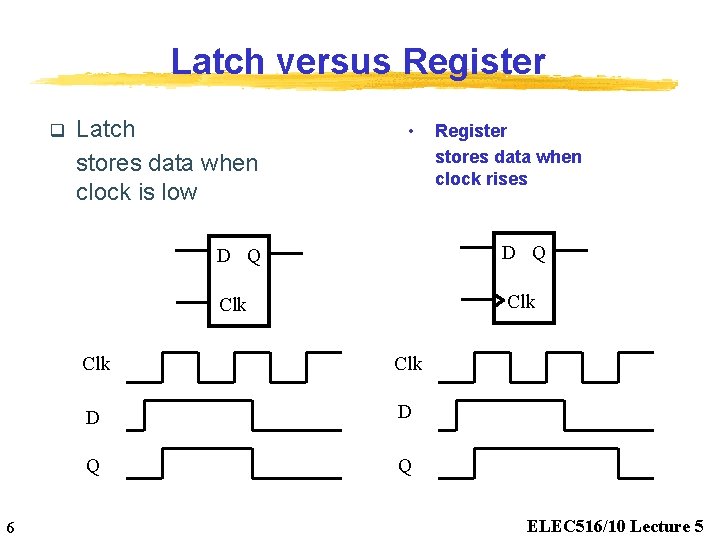
Latch versus Register q 6 Latch stores data when clock is low • Register stores data when clock rises D Q Clk Clk D D Q Q ELEC 516/10 Lecture 5

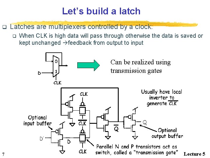
Let’s build a latch q Latches are multiplexers controlled by a clock: q When CLK is high data will pass through otherwise the data is saved or kept unchanged feedback from output to input Can be realized using transmission gates 7 ELEC 516/10 Lecture 5

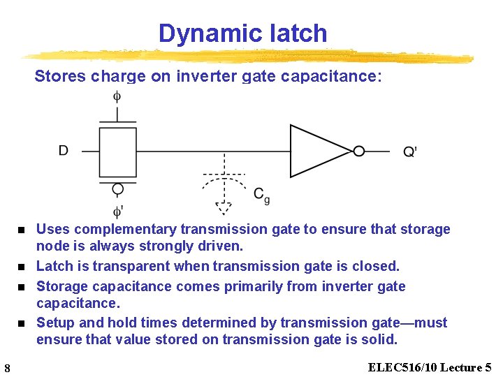
Dynamic latch Stores charge on inverter gate capacitance: n n 8 Uses complementary transmission gate to ensure that storage node is always strongly driven. Latch is transparent when transmission gate is closed. Storage capacitance comes primarily from inverter gate capacitance. Setup and hold times determined by transmission gate—must ensure that value stored on transmission gate is solid. ELEC 516/10 Lecture 5

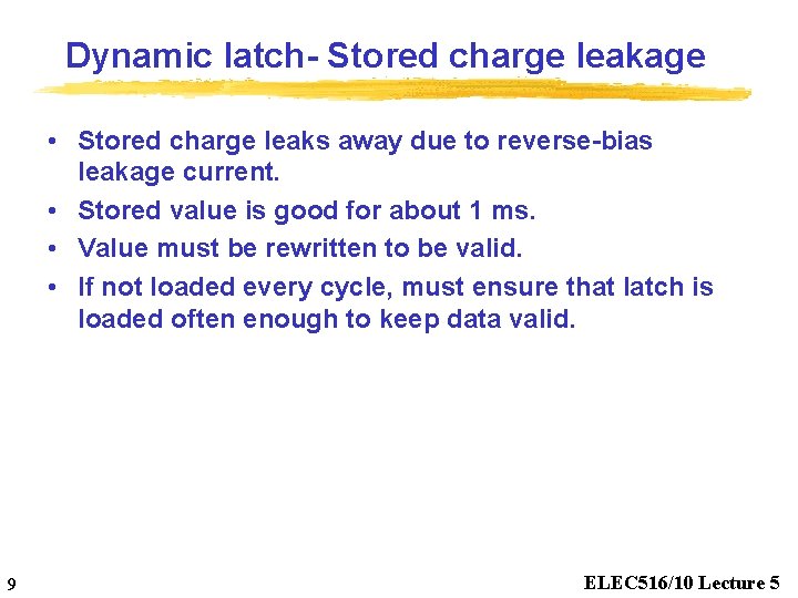
Dynamic latch- Stored charge leakage • Stored charge leaks away due to reverse-bias leakage current. • Stored value is good for about 1 ms. • Value must be rewritten to be valid. • If not loaded every cycle, must ensure that latch is loaded often enough to keep data valid. 9 ELEC 516/10 Lecture 5

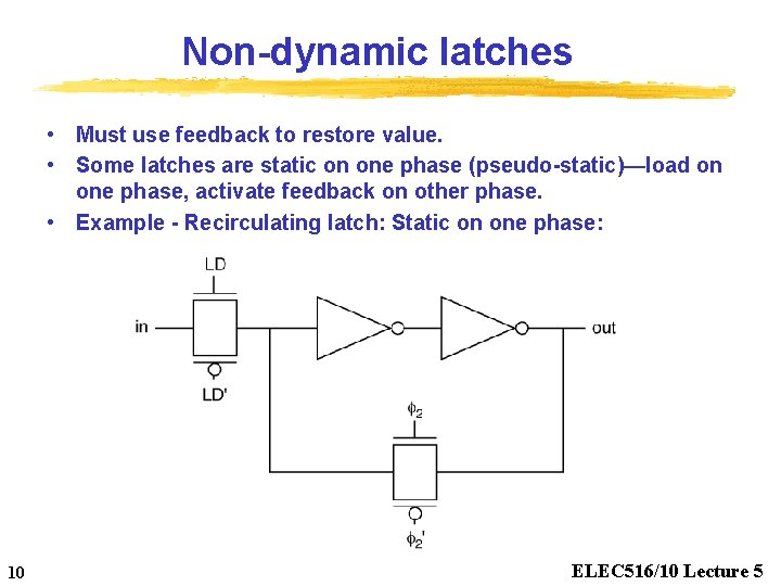
Non-dynamic latches • Must use feedback to restore value. • Some latches are static on one phase (pseudo-static)—load on one phase, activate feedback on other phase. • Example - Recirculating latch: Static on one phase: 10 ELEC 516/10 Lecture 5

Latch-Based Design • N latch is transparent when f = 0 • P latch is transparent when f = 1 f N Latch Logic P Latch Logic 11 ELEC 516/10 Lecture 5

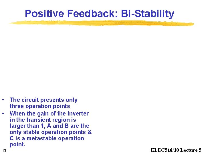
Positive Feedback: Bi-Stability • The circuit presents only three operation points • When the gain of the inverter in the transient region is larger than 1, A and B are the only stable operation points & C is a metastable operation point. 12 ELEC 516/10 Lecture 5

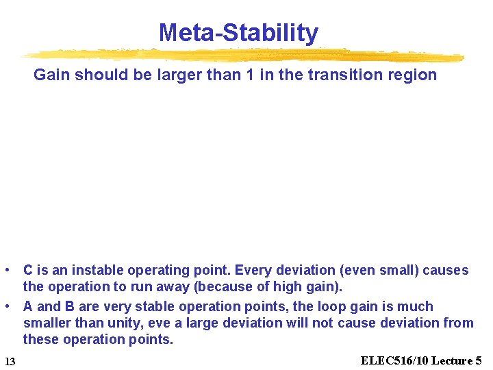
Meta-Stability Gain should be larger than 1 in the transition region • C is an instable operating point. Every deviation (even small) causes the operation to run away (because of high gain). • A and B are very stable operation points, the loop gain is much smaller than unity, eve a large deviation will not cause deviation from these operation points. 13 ELEC 516/10 Lecture 5

Flip states in Bistable Circuit • Two different approaches: – Cutting the feedback loop • Open the loop and write data • Multiplexer based • Q = Clk’. Q + Clk. In – Overpowering the feedback loop • Applying a trigger signal at the input of the flipflop to overpower the stored value to a new value • Careful sizing of the transistors in the feedback loop and the input is necessary 14 ELEC 516/10 Lecture 5

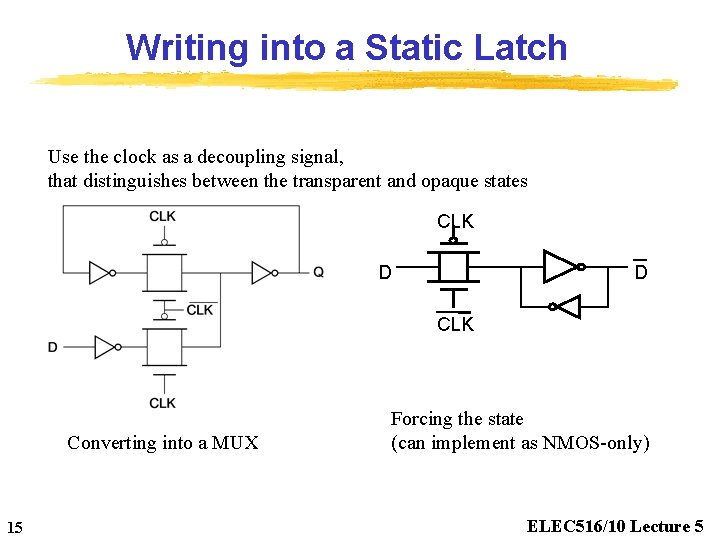
Writing into a Static Latch Use the clock as a decoupling signal, that distinguishes between the transparent and opaque states CLK D D CLK Converting into a MUX 15 Forcing the state (can implement as NMOS-only) ELEC 516/10 Lecture 5

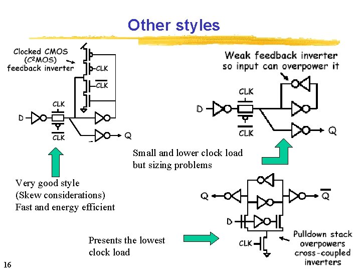
Other styles Small and lower clock load but sizing problems Very good style (Skew considerations) Fast and energy efficient Presents the lowest clock load 16 ELEC 516/10 Lecture 5

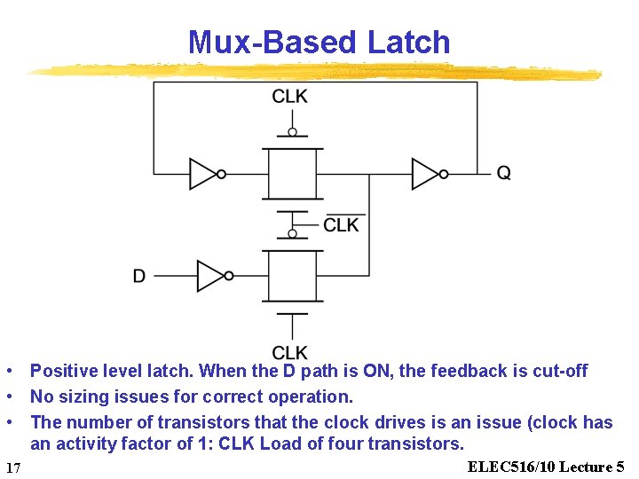
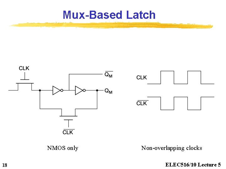
Mux-Based Latch • Positive level latch. When the D path is ON, the feedback is cut-off • No sizing issues for correct operation. • The number of transistors that the clock drives is an issue (clock has an activity factor of 1: CLK Load of four transistors. 17 ELEC 516/10 Lecture 5

Mux-Based Latch NMOS only 18 Non-overlapping clocks ELEC 516/10 Lecture 5

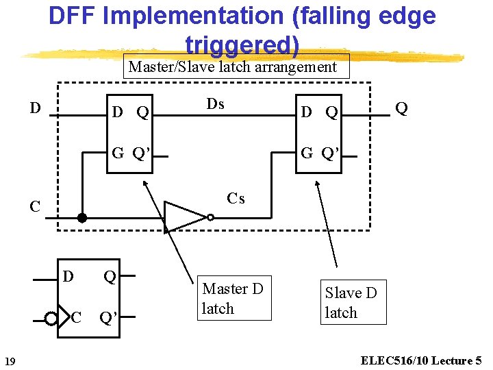
DFF Implementation (falling edge triggered) Master/Slave latch arrangement D D Q Ds G Q’ Cs C D C 19 Q D Q Q Q’ Master D latch Slave D latch ELEC 516/10 Lecture 5

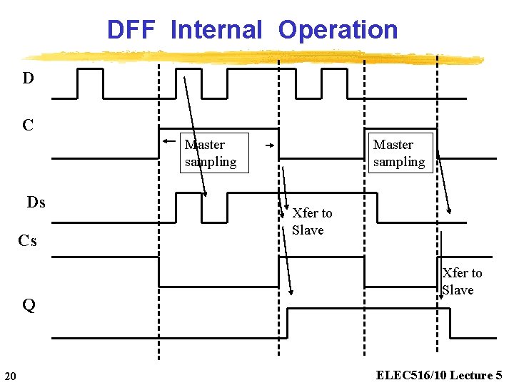
DFF Internal Operation D C Master sampling Ds Cs Q 20 Master sampling Xfer to Slave ELEC 516/10 Lecture 5

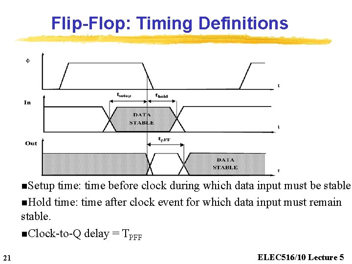
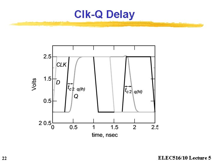
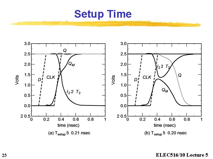
Flip-Flop: Timing Definitions n. Setup time: time before clock during which data input must be stable. n. Hold time: time after clock event for which data input must remain stable. n. Clock-to-Q delay = TPFF 21 ELEC 516/10 Lecture 5

Clk-Q Delay 22 ELEC 516/10 Lecture 5

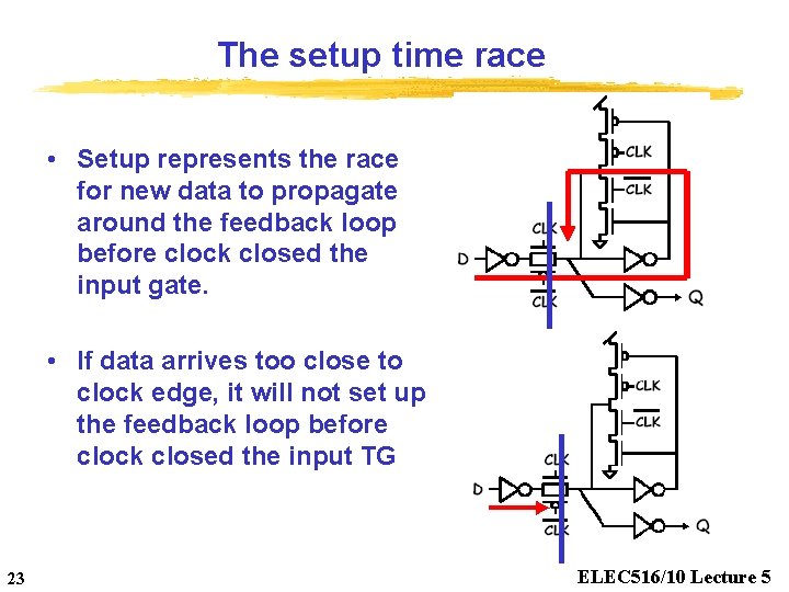
The setup time race • Setup represents the race for new data to propagate around the feedback loop before clock closed the input gate. • If data arrives too close to clock edge, it will not set up the feedback loop before clock closed the input TG 23 ELEC 516/10 Lecture 5

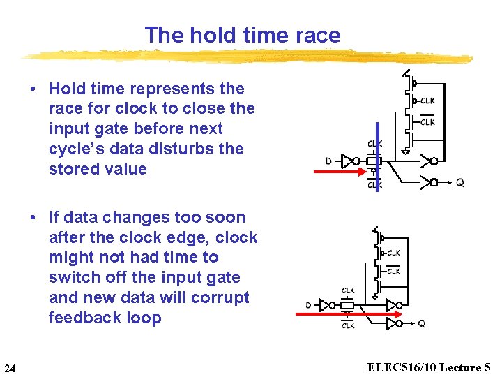
The hold time race • Hold time represents the race for clock to close the input gate before next cycle’s data disturbs the stored value • If data changes too soon after the clock edge, clock might not had time to switch off the input gate and new data will corrupt feedback loop 24 ELEC 516/10 Lecture 5

Setup Time 25 ELEC 516/10 Lecture 5

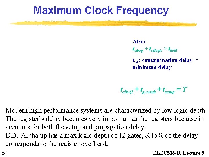
Maximum Clock Frequency Also: tcdreg + tcdlogic > thold tcd: contamination delay = minimum delay tclk-Q + tp, comb + tsetup = T Modern high performance systems are characterized by low logic depth The register’s delay becomes very important as the registers because it accounts for both the setup and propagation delay. DEC Alpha up has a max logic depth of 12 gates, &15% of the delay corresponds to the register overhead. 26 ELEC 516/10 Lecture 5

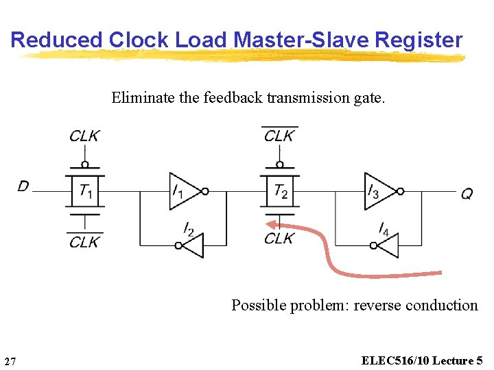
Reduced Clock Load Master-Slave Register Eliminate the feedback transmission gate. Possible problem: reverse conduction 27 ELEC 516/10 Lecture 5

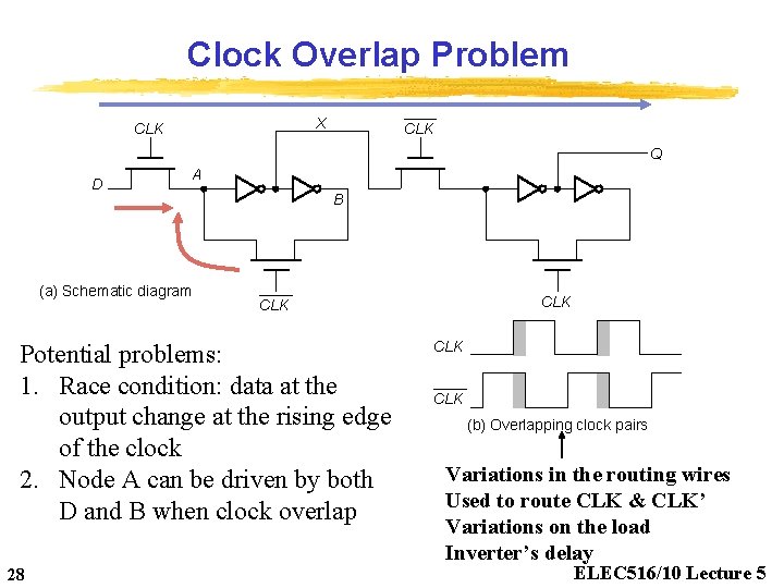
Clock Overlap Problem X CLK Q D A (a) Schematic diagram B Potential problems: 1. Race condition: data at the output change at the rising edge of the clock 2. Node A can be driven by both D and B when clock overlap 28 CLK CLK (b) Overlapping clock pairs Variations in the routing wires Used to route CLK & CLK’ Variations on the load Inverter’s delay ELEC 516/10 Lecture 5

2 phase Non-overlapping clock DFF Two-phase non-overlapping clocks 29 ELEC 516/10 Lecture 5

6 Transistor CMOS SR-Flip Flop 30 ELEC 516/10 Lecture 5

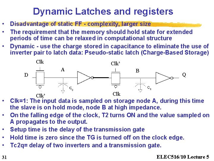
Dynamic Latches and registers • Disadvantage of static FF - complexity, larger size • The requirement that the memory should hold state for extended periods of time can be relaxed in computational structure • Dynamic - use the charge stored in capacitance to eliminate the use of inverter pair to latch data: Pseudo-static latch (Charge-Based Storage) Clk’ A D Clk’ B Q Clk • Clk=1: The input data is sampled on storage node A, during this time the slave is on hold mode, node B at high impedance. • On the falling edge of the clock, T 2 turns ON and the value sampled on A propagates to the output. • Setup time is the delay of the transmission gate • Hold time is zero since the TG is turned off on the clock edge. • Tc 2 q= delay of two inverters and a transmission gate. 31 ELEC 516/10 Lecture 5

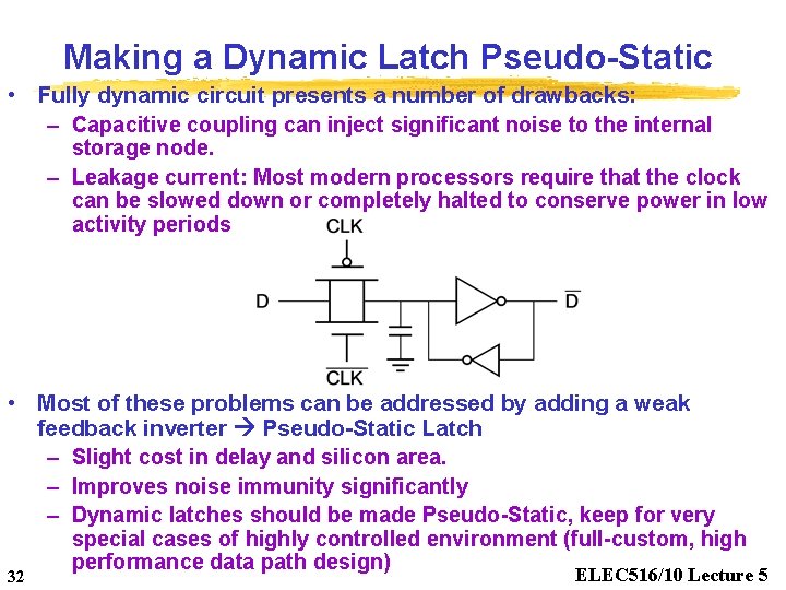
Making a Dynamic Latch Pseudo-Static • Fully dynamic circuit presents a number of drawbacks: – Capacitive coupling can inject significant noise to the internal storage node. – Leakage current: Most modern processors require that the clock can be slowed down or completely halted to conserve power in low activity periods • Most of these problems can be addressed by adding a weak feedback inverter Pseudo-Static Latch – Slight cost in delay and silicon area. – Improves noise immunity significantly – Dynamic latches should be made Pseudo-Static, keep for very 32 special cases of highly controlled environment (full-custom, high performance data path design) ELEC 516/10 Lecture 5

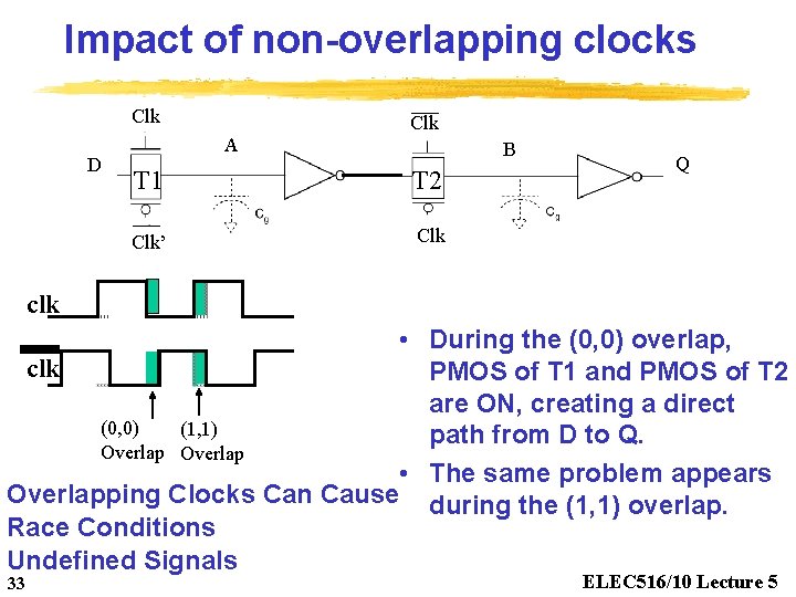
Impact of non-overlapping clocks Clk D Clk A B T 1 T 2 Clk’ Clk Q clk • During the (0, 0) overlap, clk PMOS of T 1 and PMOS of T 2 are ON, creating a direct (0, 0) (1, 1) path from D to Q. Overlap • The same problem appears Overlapping Clocks Can Cause during the (1, 1) overlap. Race Conditions Undefined Signals 33 ELEC 516/10 Lecture 5

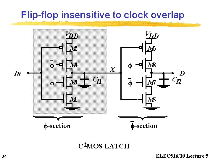
Flip-flop insensitive to clock overlap f VDD M 2 M 6 M 4 In f M 3 X CL 1 f f M 1 M 8 M 7 D CL 2 M 5 f-section C 2 MOS LATCH 34 ELEC 516/10 Lecture 5

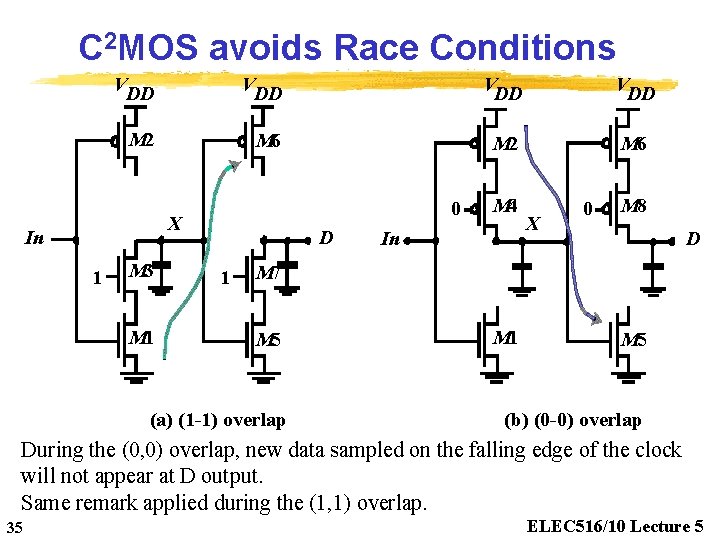
C 2 MOS avoids Race Conditions VDD VDD M 2 M 6 0 X In 1 M 3 M 1 D 1 M 4 In X 0 M 8 D M 7 M 5 (a) (1 -1) overlap M 1 M 5 (b) (0 -0) overlap During the (0, 0) overlap, new data sampled on the falling edge of the clock will not appear at D output. Same remark applied during the (1, 1) overlap. 35 ELEC 516/10 Lecture 5

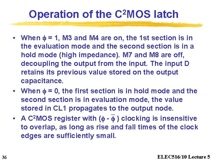
Operation of the C 2 MOS latch • When f = 1, M 3 and M 4 are on, the 1 st section is in the evaluation mode and the second section is in a hold mode (high impedance). M 7 and M 8 are off, decoupling the output from the input. The input D retains its previous value stored on the output capacitance. • When f = 0, the first section is in hold mode and the second section is in evaluation mode, the value stored in CL 1 propagates to the output node. • A C 2 MOS register with (f - f ) clocking is insensitive to overlap, as long as rise and fall times of the clock edges are sufficiently small. 36 ELEC 516/10 Lecture 5

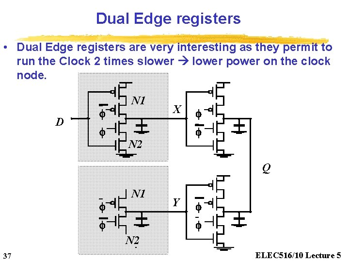
Dual Edge registers • Dual Edge registers are very interesting as they permit to run the Clock 2 times slower power on the clock node. D f f N 1 X f f N 2 Q f N 1 f Y f f N 2 37 ELEC 516/10 Lecture 5

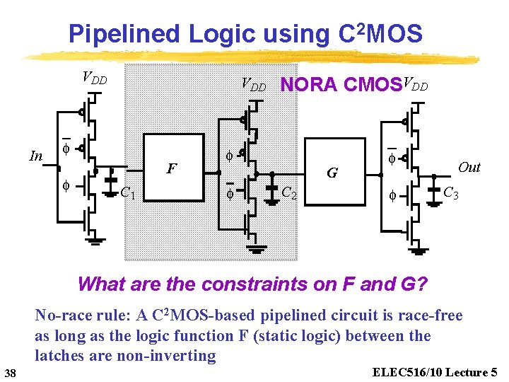
Pipelined Logic using C 2 MOS VDD In VDD f f F C 1 NORA CMOSVDD f G f C 2 f f Out C 3 What are the constraints on F and G? No-race rule: A C 2 MOS-based pipelined circuit is race-free as long as the logic function F (static logic) between the latches are non-inverting 38 ELEC 516/10 Lecture 5

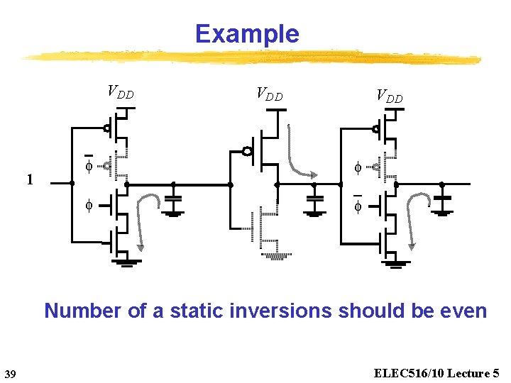
Example VDD 1 VDD f f Number of a static inversions should be even 39 ELEC 516/10 Lecture 5

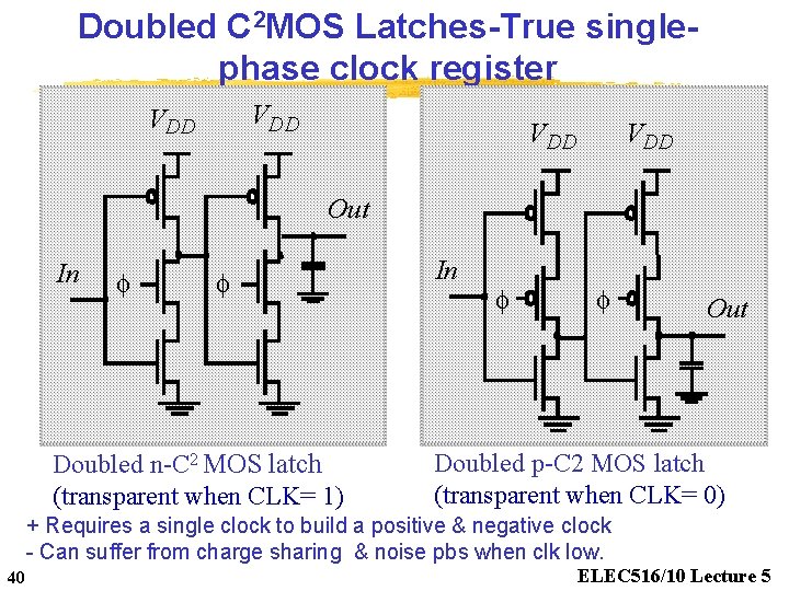
Doubled C 2 MOS Latches-True singlephase clock register VDD VDD Out In f f Doubled n-C 2 MOS latch (transparent when CLK= 1) In f f Out Doubled p-C 2 MOS latch (transparent when CLK= 0) + Requires a single clock to build a positive & negative clock - Can suffer from charge sharing & noise pbs when clk low. 40 ELEC 516/10 Lecture 5

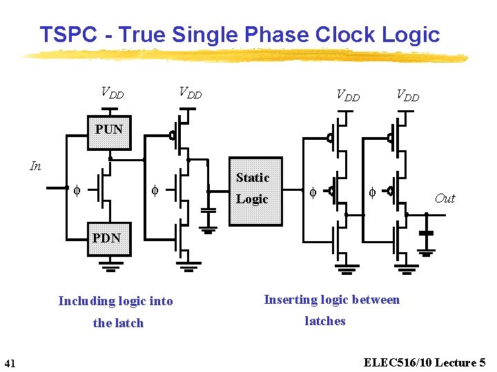
TSPC - True Single Phase Clock Logic VDD VDD PUN In f f Static Logic f f Out PDN Including logic into the latch 41 Inserting logic between latches ELEC 516/10 Lecture 5

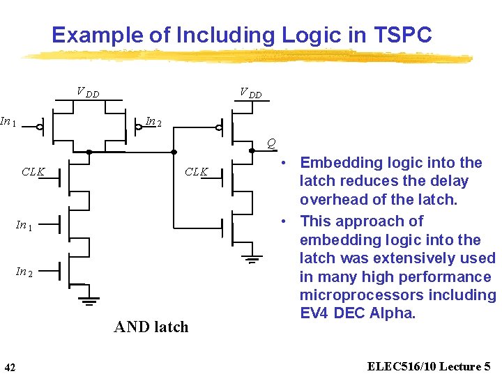
Example of Including Logic in TSPC V DD In 1 V DD In 2 Q CLK In 1 In 2 AND latch 42 • Embedding logic into the latch reduces the delay overhead of the latch. • This approach of embedding logic into the latch was extensively used in many high performance microprocessors including EV 4 DEC Alpha. ELEC 516/10 Lecture 5

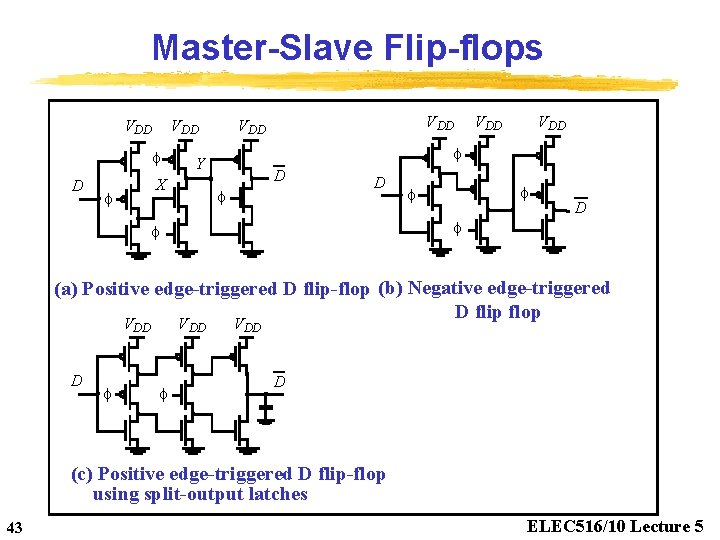
Master-Slave Flip-flops VDD V DD f Y X V DD D f f (a) Positive edge-triggered D flip-flop (b) Negative edge-triggered D flip flop VDD D f V DD D (c) Positive edge-triggered D flip-flop using split-output latches 43 ELEC 516/10 Lecture 5

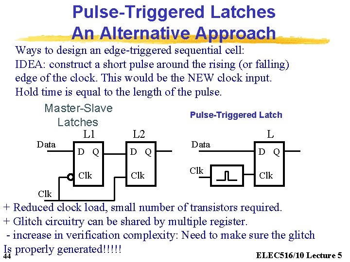
Pulse-Triggered Latches An Alternative Approach Ways to design an edge-triggered sequential cell: IDEA: construct a short pulse around the rising (or falling) edge of the clock. This would be the NEW clock input. Hold time is equal to the length of the pulse. Master-Slave Pulse-Triggered Latches L 1 L 2 L Data D Q Clk Data Clk D Q Clk + Reduced clock load, small number of transistors required. + Glitch circuitry can be shared by multiple register. - increase in verification complexity: Need to make sure the glitch Is properly generated!!!!! ELEC 516/10 Lecture 5 44

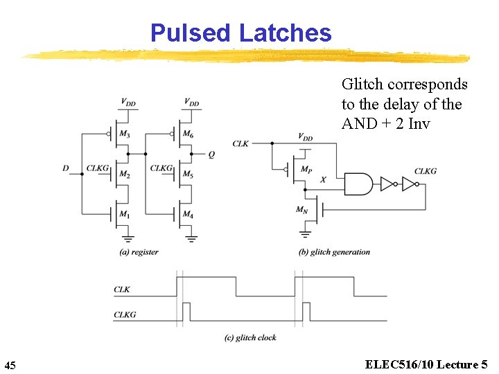
Pulsed Latches Glitch corresponds to the delay of the AND + 2 Inv 45 ELEC 516/10 Lecture 5

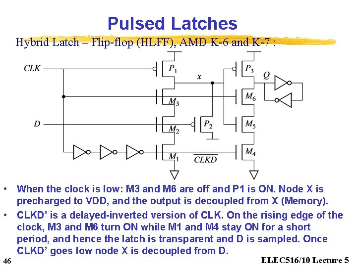
Pulsed Latches Hybrid Latch – Flip-flop (HLFF), AMD K-6 and K-7 : • When the clock is low: M 3 and M 6 are off and P 1 is ON. Node X is precharged to VDD, and the output is decoupled from X (Memory). • CLKD’ is a delayed-inverted version of CLK. On the rising edge of the clock, M 3 and M 6 turn ON while M 1 and M 4 stay ON for a short period, and hence the latch is transparent and D is sampled. Once CLKD’ goes low node X is decoupled from D. 46 ELEC 516/10 Lecture 5

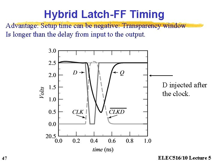
Hybrid Latch-FF Timing Advantage: Setup time can be negative: Transparency window Is longer than the delay from input to the output. D injected after the clock. 47 ELEC 516/10 Lecture 5

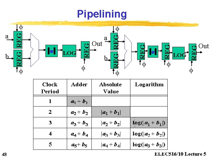
Pipelining f 48 f f f LOG REG f REG b REG LOG Out a REG b f REG a REG f Out f ELEC 516/10 Lecture 5

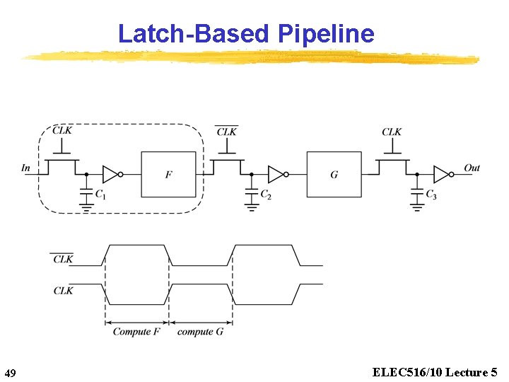
Latch-Based Pipeline 49 ELEC 516/10 Lecture 5

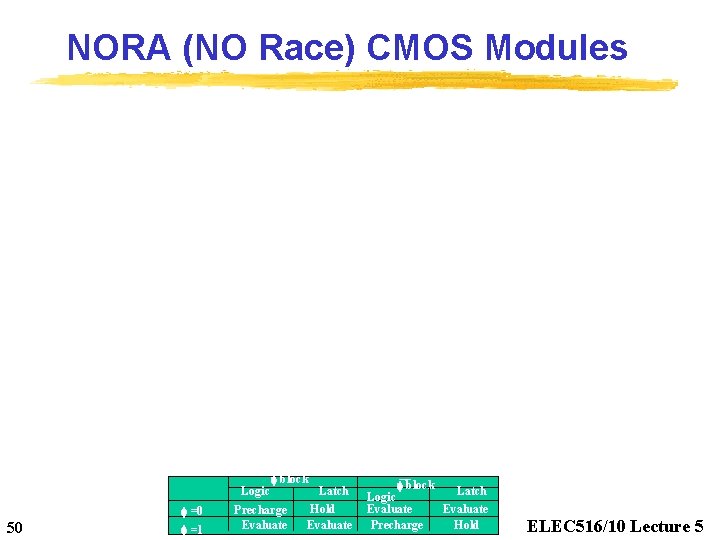
NORA (NO Race) CMOS Modules Logic f =0 50 f =1 f block Precharge Evaluate Latch Hold Evaluate f block Latch Logic Evaluate Precharge Hold ELEC 516/10 Lecture 5

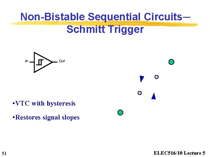
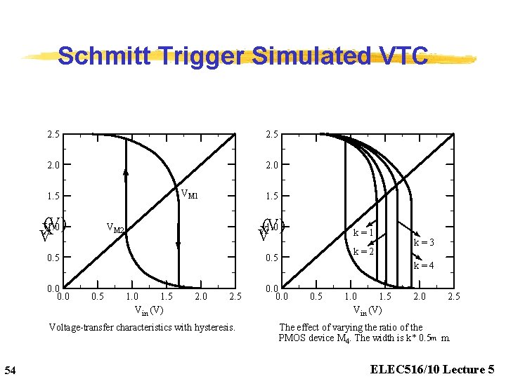
Non-Bistable Sequential Circuits─ Schmitt Trigger • VTC with hysteresis • Restores signal slopes 51 ELEC 516/10 Lecture 5

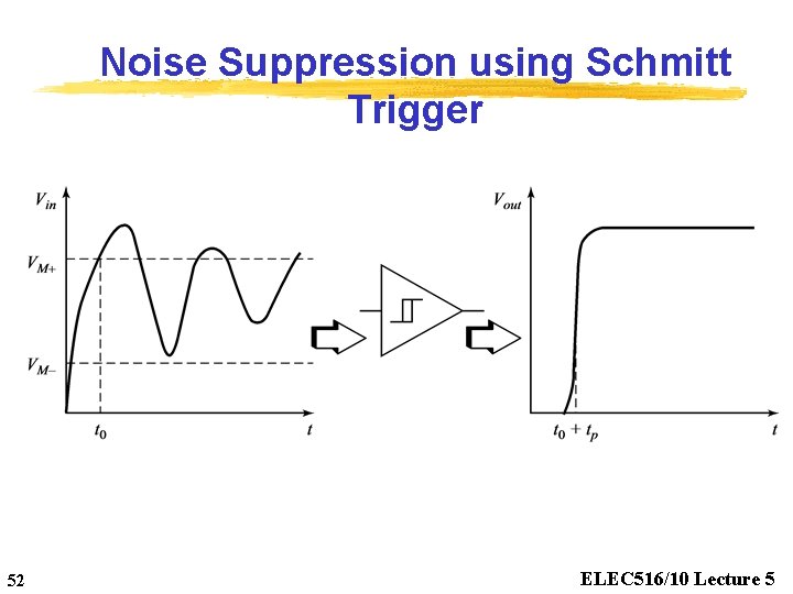
Noise Suppression using Schmitt Trigger 52 ELEC 516/10 Lecture 5

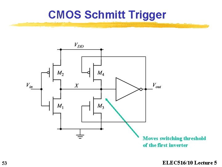
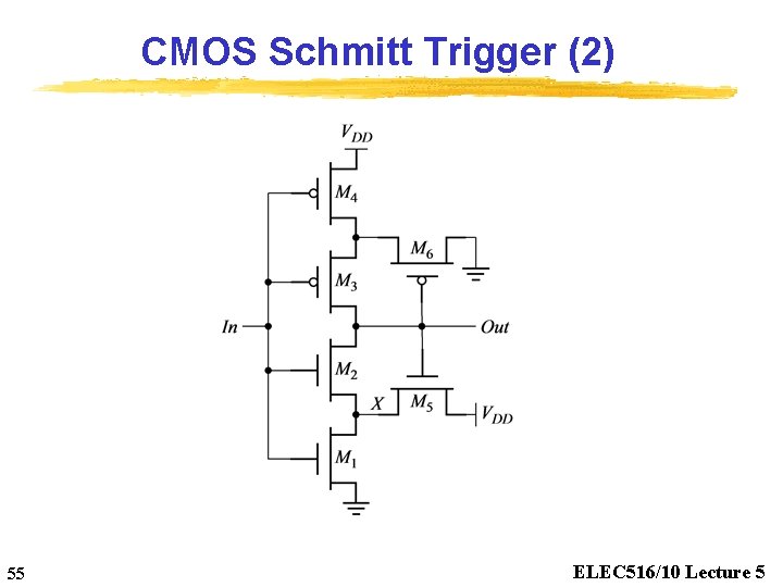
CMOS Schmitt Trigger Moves switching threshold of the first inverter 53 ELEC 516/10 Lecture 5

Schmitt Trigger Simulated VTC 2. 5 2. 0 VM 1 1. 5 (V) 1. 0 X V 1. 5 (V) 1. 0 x V VM 2 0. 5 0. 0 k=2 0. 5 1. 0 1. 5 Vin (V) 2. 0 2. 5 Voltage-transfer characteristics with hysteresis. 54 k=1 k=3 k=4 0. 0 0. 5 1. 0 1. 5 Vin (V) 2. 0 2. 5 The effect of varying the ratio of the PMOS device M 4. The width is k* 0. 5 m m. ELEC 516/10 Lecture 5

CMOS Schmitt Trigger (2) 55 ELEC 516/10 Lecture 5

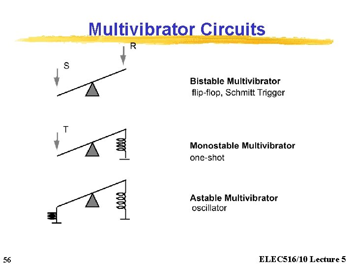
Multivibrator Circuits 56 ELEC 516/10 Lecture 5

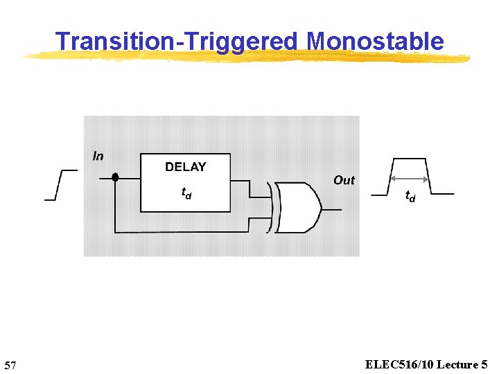
Transition-Triggered Monostable 57 ELEC 516/10 Lecture 5

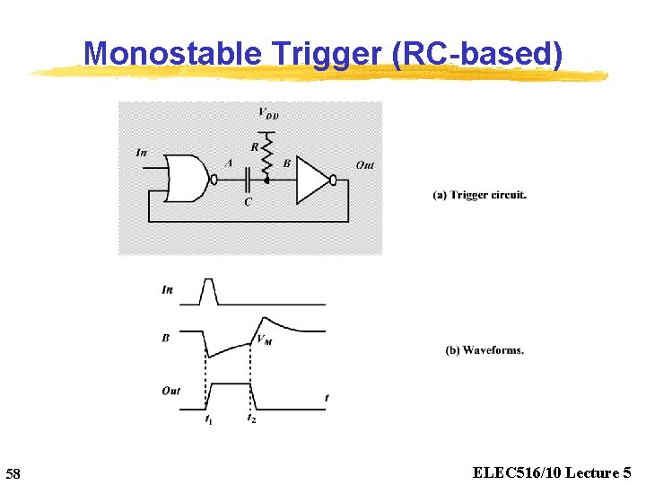
Monostable Trigger (RC-based) 58 ELEC 516/10 Lecture 5

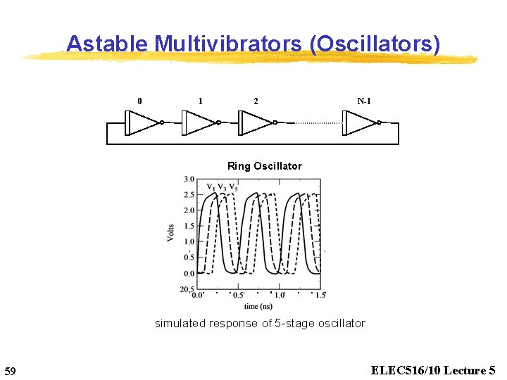
Astable Multivibrators (Oscillators) 0 1 2 N-1 Ring Oscillator simulated response of 5 -stage oscillator 59 ELEC 516/10 Lecture 5

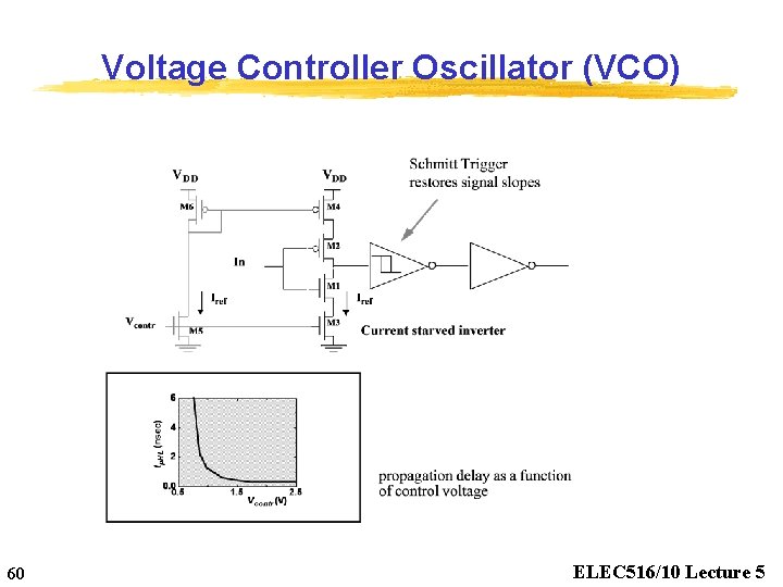
Voltage Controller Oscillator (VCO) 60 ELEC 516/10 Lecture 5

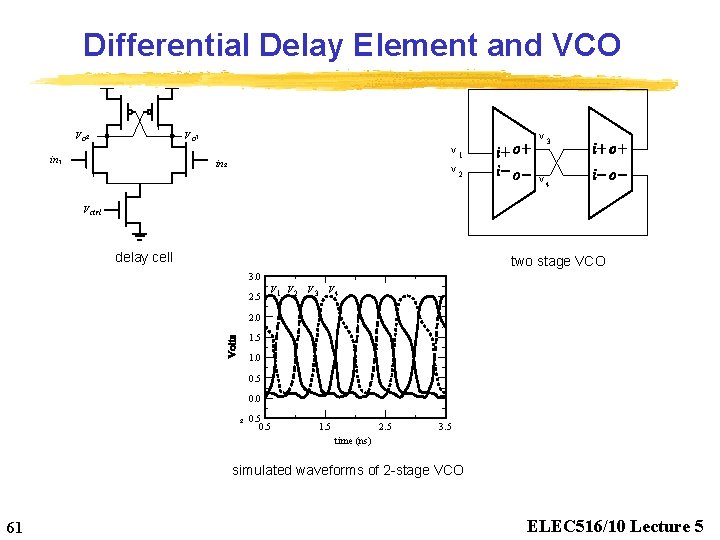
Differential Delay Element and VCO V o 2 V o 1 in 1 v 1 in 2 v 3 v 4 V ctrl delay cell two stage VCO 3. 0 2. 5 V 1 V 2 V 3 V 4 2. 0 1. 5 1. 0 0. 5 0. 0 2 0. 5 1. 5 2. 5 3. 5 time (ns) simulated waveforms of 2 -stage VCO 61 ELEC 516/10 Lecture 5