
ELE 22 MIC Lecture 14 15 Edge Detector

- Slides: 56
ELE 22 MIC Lecture 14 & 15 • Edge Detector • Latch vs Flip Flop – S-R Latch, Transparent D-Latch – Clocked D-Latch – J-K Flip Flop, Toggle Flip Flop • Flip Flop Applications – Register/Memory, Shift Register, Counter • 68 HC 11 Analog to Digital Converter • Variable Speed Stepper Motor Application
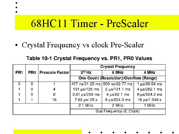
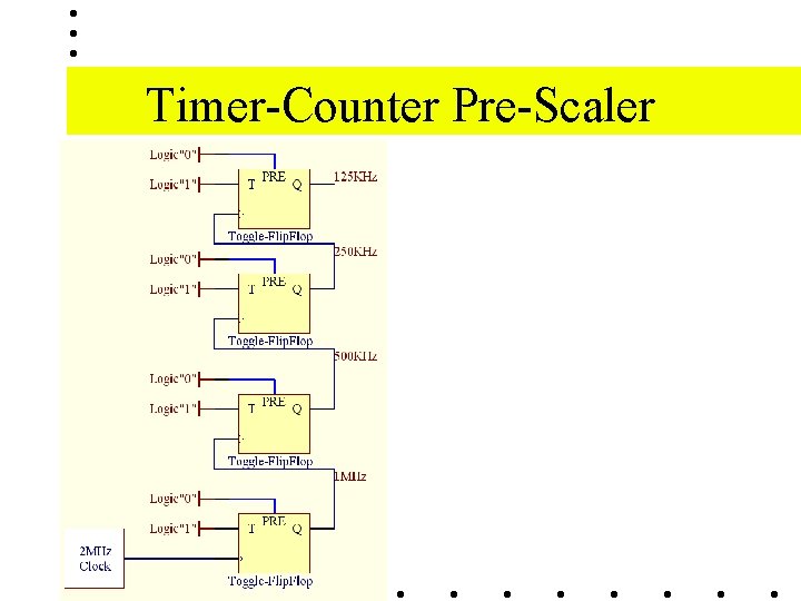
68 HC 11 Timer - Pre. Scaler • Crystal Frequency vs clock Pre-Scaler
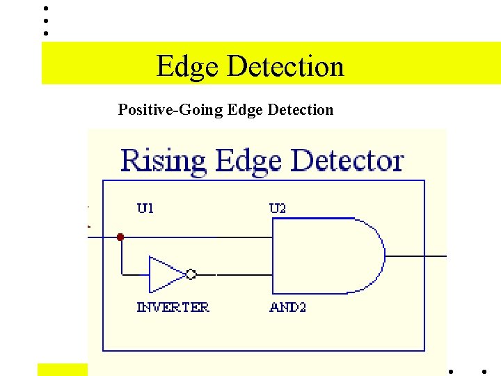
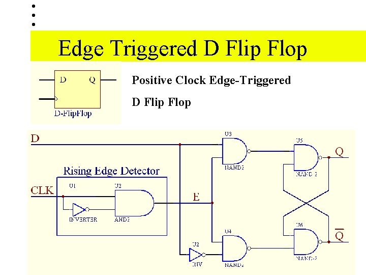
Edge Detection Positive-Going Edge Detection
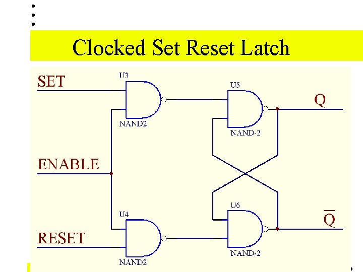
Clocked Set Reset Latch
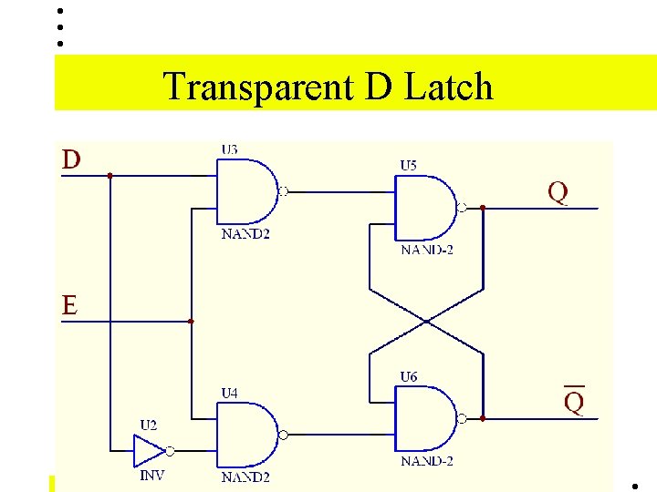
Transparent D Latch
Edge Triggered D Flip Flop Positive Clock Edge-Triggered D Flip Flop
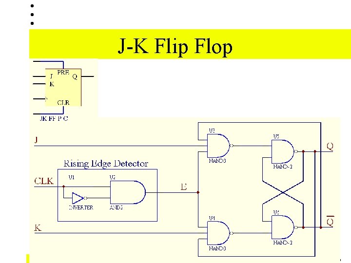
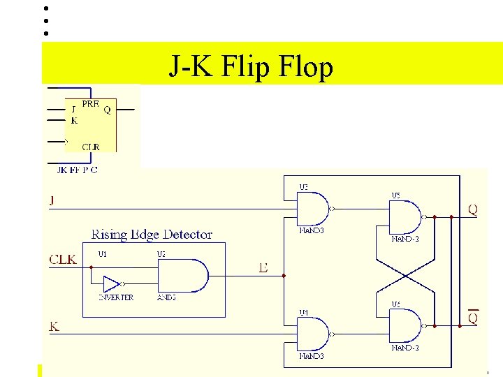
J-K Flip Flop
J-K Flip Flop
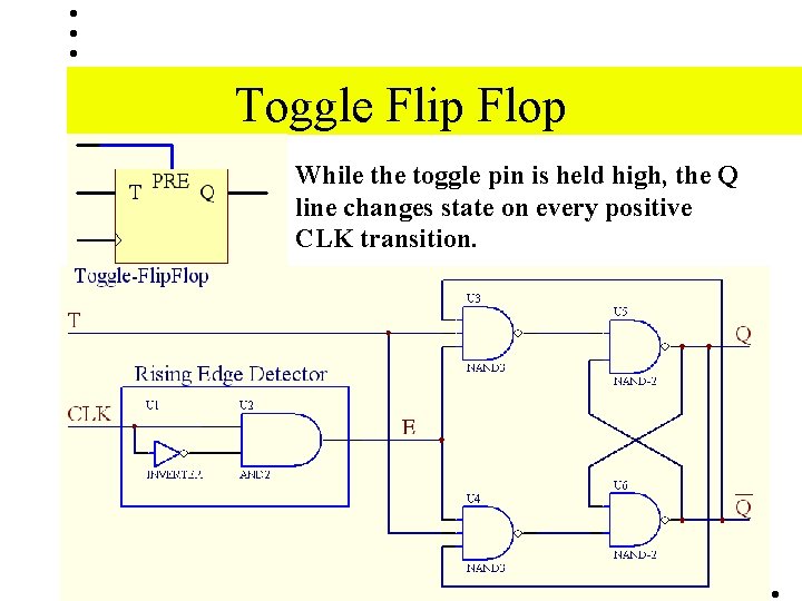
Toggle Flip Flop While the toggle pin is held high, the Q line changes state on every positive CLK transition.
4 Bit - Ripple Counter
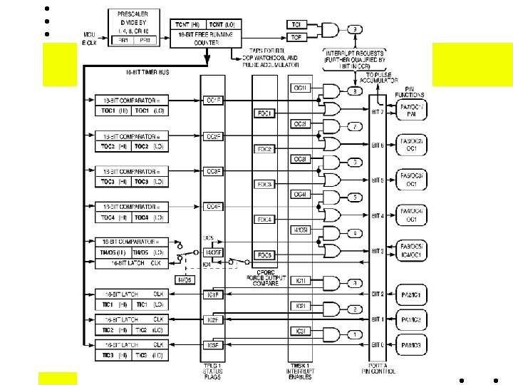
Timer-Counter Pre-Scaler
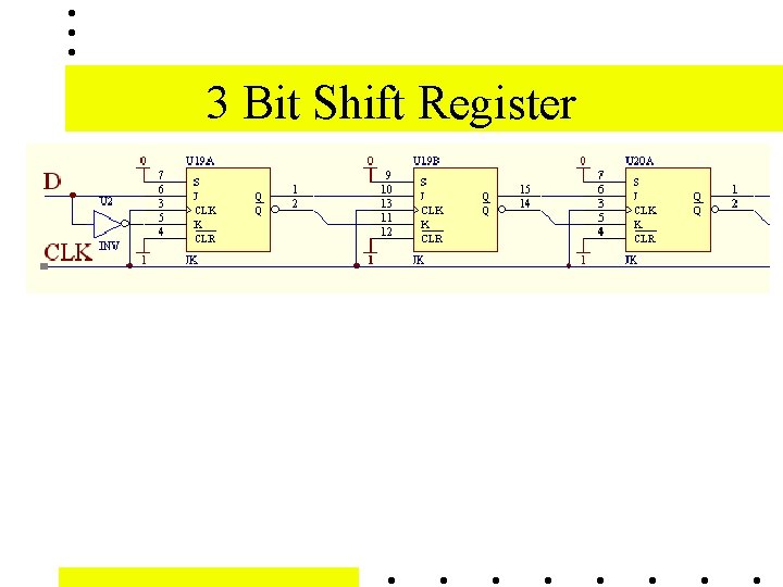
3 Bit Shift Register
Variable Speed Stepper Motor • The next application we will look at is a Variable Speed Stepper Motor control • The forward/reverse speed is controlled by a potentiometer connected to the ADC input
Variable Speed Stepper Motor • The unsigned potentiometer value is biased by 128 so that mid-way = 0 speed, 255 = full speed forwards, -255 = full speed reverse. • The stepper motor coil activation sequence is controlled by four output lines of Port A
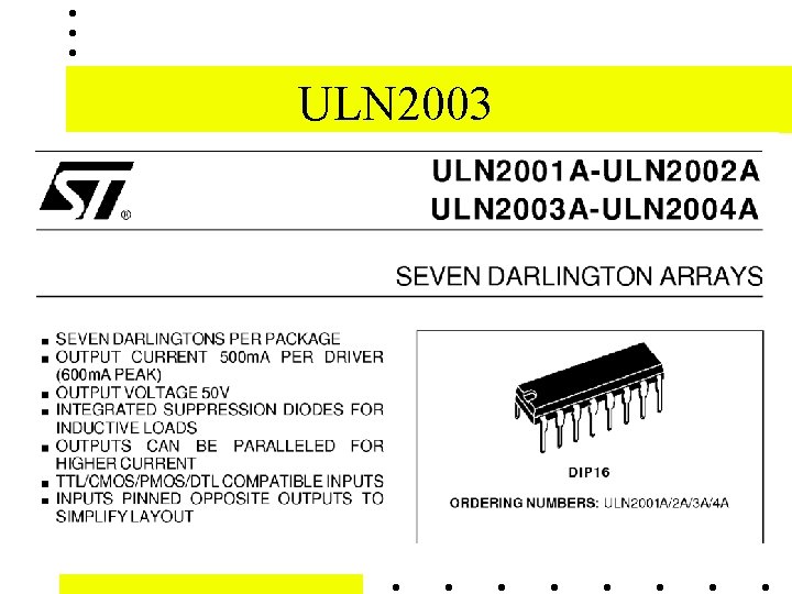
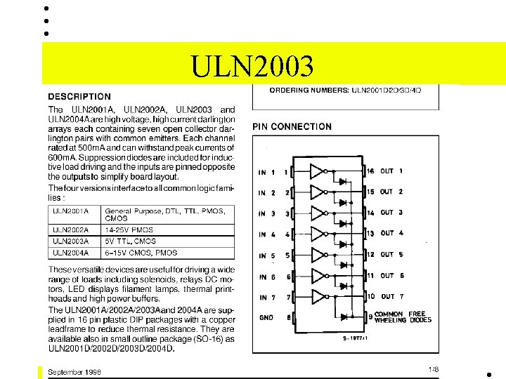
ULN 2003
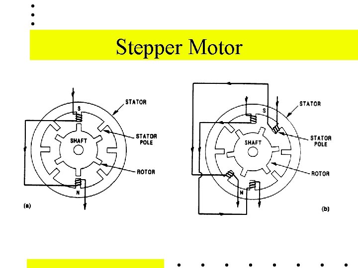
Stepper Motor
ULN 2003
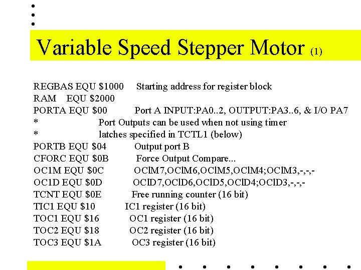
Variable Speed Stepper Motor (1) REGBAS EQU $1000 Starting address for register block RAM EQU $2000 PORTA EQU $00 Port A INPUT: PA 0. . 2, OUTPUT: PA 3. . 6, & I/O PA 7 * Port Outputs can be used when not using timer * latches specified in TCTL 1 (below) PORTB EQU $04 Output port B CFORC EQU $0 B Force Output Compare. . . OC 1 M EQU $0 C OCl. M 7, OCl. M 6, OCl. M 5, OCl. M 4; OCl. M 3, -, -, OC 1 D EQU $0 D OCl. D 7, OCl. D 6, OCl. D 5, OCl. D 4; OCl. D 3, -, -, TCNT EQU $0 E Free running counter (16 bit) TIC 1 EQU $10 IC 1 register (16 bit) TOC 1 EQU $16 OC 1 register (16 bit) TOC 2 EQU $18 OC 2 register (16 bit) TOC 3 EQU $1 A OC 3 register (16 bit)
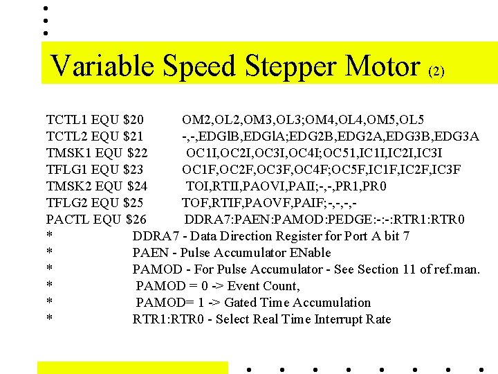
Variable Speed Stepper Motor (2) TCTL 1 EQU $20 OM 2, OL 2, OM 3, OL 3; OM 4, OL 4, OM 5, OL 5 TCTL 2 EQU $21 -, -, EDGl. B, EDGl. A; EDG 2 B, EDG 2 A, EDG 3 B, EDG 3 A TMSK 1 EQU $22 OC 1 I, OC 2 I, OC 3 I, OC 4 I; OC 51, IC 1 I, IC 2 I, IC 3 I TFLG 1 EQU $23 OC 1 F, OC 2 F, OC 3 F, OC 4 F; OC 5 F, IC 1 F, IC 2 F, IC 3 F TMSK 2 EQU $24 TOI, RTII, PAOVI, PAII; -, -, PR 1, PR 0 TFLG 2 EQU $25 TOF, RTIF, PAOVF, PAIF; -, -, -, PACTL EQU $26 DDRA 7: PAEN: PAMOD: PEDGE: -: -: RTR 1: RTR 0 * DDRA 7 - Data Direction Register for Port A bit 7 * PAEN - Pulse Accumulator ENable * PAMOD - For Pulse Accumulator - See Section 11 of ref. man. * PAMOD = 0 -> Event Count, * PAMOD= 1 -> Gated Time Accumulation * RTR 1: RTR 0 - Select Real Time Interrupt Rate
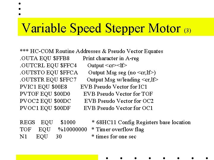
Variable Speed Stepper Motor (3) *** HC-COM Routine Addresses & Pseudo Vector Equates. OUTA EQU $FFB 8 Print character in A-reg. OUTCRL EQU $FFC 4 Output <cr><lf>. OUTSTO EQU $FFCA Output Msg seg (no <cr, lf>). OUTSTR EQU $FFC 7 Output Msg w/leading <cr, lf> PVIC 1 EQU $00 E 8 EVB Pseudo Vector for IC 1 PVTOF EQU $00 D 0 EVB Pseudo Vector for TOF PVOC 2 EQU $00 DC EVB Pseudo Vector for OC 2 PVOC 1 EQU $00 DF EVB Pseudo Vector for OC 1 REGS EQU $1000 * 68 HC 11 Config Registers base location TOF EQU %10000000 * Timer overflow flag N 1 EQU 30 * times for one sec
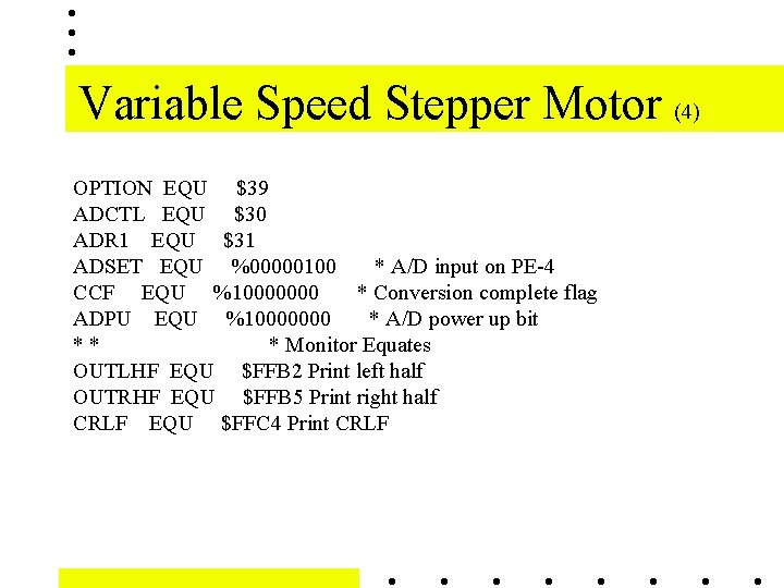
Variable Speed Stepper Motor (4) OPTION EQU $39 ADCTL EQU $30 ADR 1 EQU $31 ADSET EQU %00000100 * A/D input on PE-4 CCF EQU %10000000 * Conversion complete flag ADPU EQU %10000000 * A/D power up bit ** * Monitor Equates OUTLHF EQU $FFB 2 Print left half OUTRHF EQU $FFB 5 Print right half CRLF EQU $FFC 4 Print CRLF
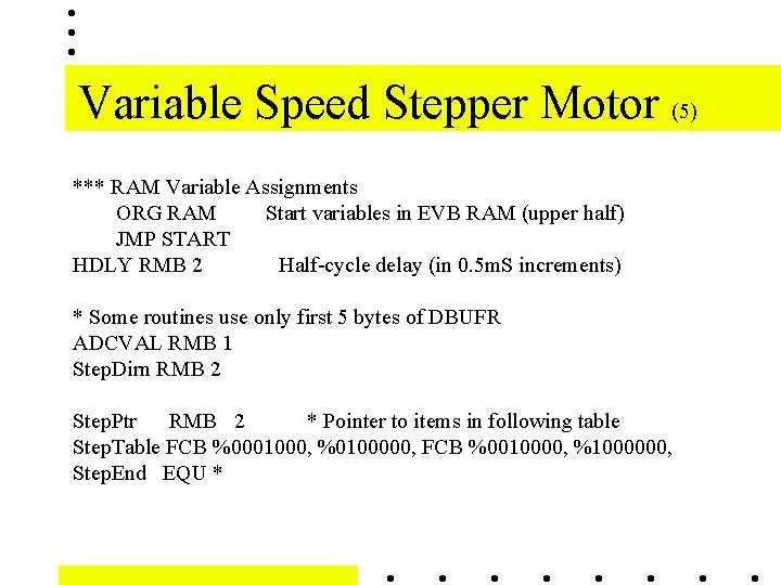
Variable Speed Stepper Motor (5) *** RAM Variable Assignments ORG RAM Start variables in EVB RAM (upper half) JMP START HDLY RMB 2 Half-cycle delay (in 0. 5 m. S increments) * Some routines use only first 5 bytes of DBUFR ADCVAL RMB 1 Step. Dirn RMB 2 Step. Ptr RMB 2 * Pointer to items in following table Step. Table FCB %0001000, %0100000, FCB %0010000, %1000000, Step. End EQU *
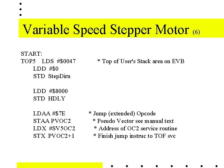
Variable Speed Stepper Motor (6) START: TOP 5 LDS #$0047 LDD #$0 STD Step. Dirn * Top of User's Stack area on EVB LDD #$8000 STD HDLY LDAA #$7 E STAA PVOC 2 LDX #SV 5 OC 2 STX PVOC 2+1 * Jump (extended) Opcode * Pseudo Vector see manual text * Address of OC 2 service routine * Finish jump instruc to TOF svc
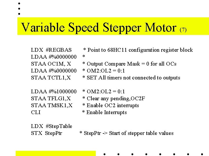
Variable Speed Stepper Motor (7) LDX #REGBAS * Point to 68 HC 11 configuration register block LDAA #%0000000 * STAA OC 1 M, X * Output Compare Mask = 0 for all OCs LDAA #%0000000 * OM 2: OL 2 = 0: 1 STAA TCTL 1, X * SET All timers not connected to outputs LDAA #%1000000 * OM 2: OL 2 = 0: 1 STAA TFLG 1, X * Clear any pending, OC 2 F STAA TMSK 1, X * Enable OC 2 interrupts CLI * Enable Interrupts LDX #Step. Table STX Step. Ptr * Step. Ptr -> Start of stepper table values
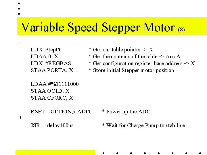
Variable Speed Stepper Motor (8) LDX Step. Ptr LDAA 0, X LDX #REGBAS STAA PORTA, X * Get our table pointer -> X * Get the contents of the table -> Acc A * Get configuration register base address -> X * Store initial Stepper motor position LDAA #%11111000 STAA OC 1 D, X STAA CFORC, X BSET OPTION, x ADPU * Power up the ADC * JSR delay 100 us * Wait for Charge Pump to stabilise
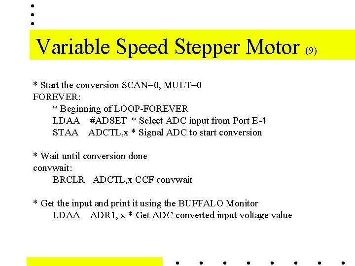
Variable Speed Stepper Motor (9) * Start the conversion SCAN=0, MULT=0 FOREVER: * Beginning of LOOP-FOREVER LDAA #ADSET * Select ADC input from Port E-4 STAA ADCTL, x * Signal ADC to start conversion * Wait until conversion done convwait: BRCLR ADCTL, x CCF convwait * Get the input and print it using the BUFFALO Monitor LDAA ADR 1, x * Get ADC converted input voltage value
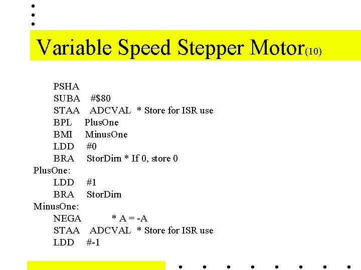
Variable Speed Stepper Motor(10) PSHA SUBA STAA BPL BMI LDD BRA Plus. One: LDD BRA Minus. One: NEGA STAA LDD #$80 ADCVAL * Store for ISR use Plus. One Minus. One #0 Stor. Dirn * If 0, store 0 #1 Stor. Dirn * A = -A ADCVAL * Store for ISR use #-1
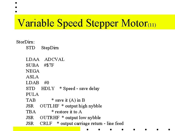
Variable Speed Stepper Motor(11) Stor. Dirn: STD Step. Dirn LDAA ADCVAL SUBA #$7 F NEGA ASLA LDAB #0 STD HDLY * Speed - save delay PULA TAB * save it (A) in B JSR OUTLHF * output high nybble TBA * restore it to A JSR OUTRHF * output low nybble JSR CRLF * output carriage return - line feed
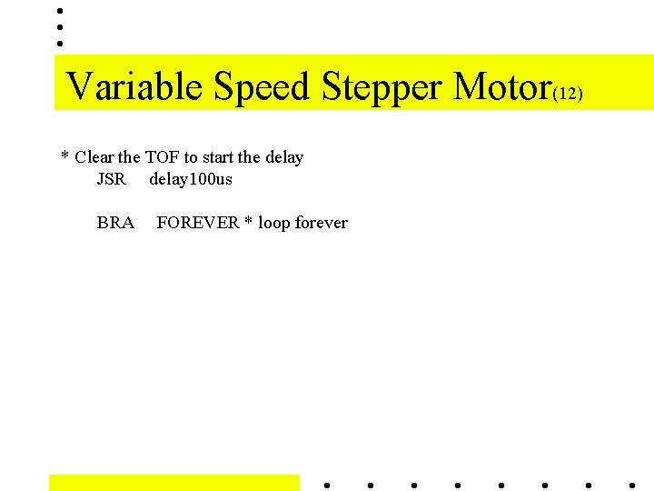
Variable Speed Stepper Motor(12) * Clear the TOF to start the delay JSR delay 100 us BRA FOREVER * loop forever
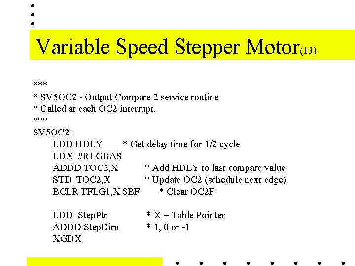
Variable Speed Stepper Motor(13) *** * SV 5 OC 2 - Output Compare 2 service routine * Called at each OC 2 interrupt. *** SV 5 OC 2: LDD HDLY * Get delay time for 1/2 cycle LDX #REGBAS ADDD TOC 2, X * Add HDLY to last compare value STD TOC 2, X * Update OC 2 (schedule next edge) BCLR TFLG 1, X $BF * Clear OC 2 F LDD Step. Ptr ADDD Step. Dirn XGDX * X = Table Pointer * 1, 0 or -1
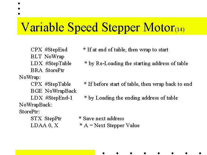
Variable Speed Stepper Motor(14) CPX #Step. End * If at end of table, then wrap to start BLT No. Wrap LDX #Step. Table * by Re-Loading the starting address of table BRA Store. Ptr No. Wrap: CPX #Step. Table * If before start of table, then wrap back to end BGE No. Wrap. Back LDX #Step. End-1 * by Loading the ending address of table No. Wrap. Back: Store. Ptr: STX Step. Ptr * Save next address LDAA 0, X * A = Next Stepper Value
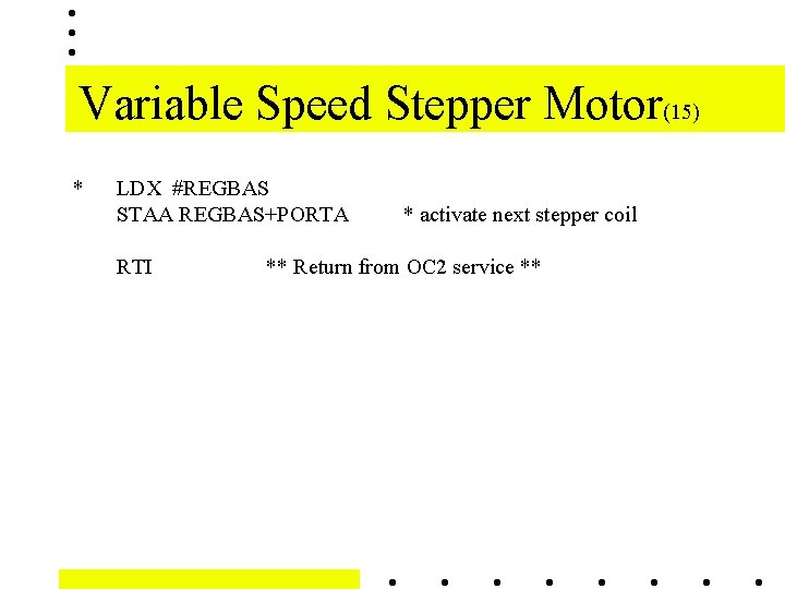
Variable Speed Stepper Motor(15) * LDX #REGBAS STAA REGBAS+PORTA RTI * activate next stepper coil ** Return from OC 2 service **
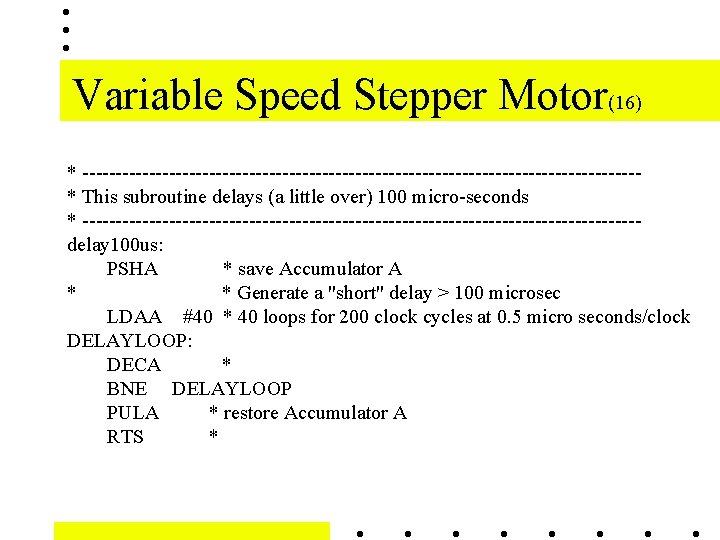
Variable Speed Stepper Motor(16) * ------------------------------------------* This subroutine delays (a little over) 100 micro-seconds * ------------------------------------------delay 100 us: PSHA * save Accumulator A * * Generate a "short" delay > 100 microsec LDAA #40 * 40 loops for 200 clock cycles at 0. 5 micro seconds/clock DELAYLOOP: DECA * BNE DELAYLOOP PULA * restore Accumulator A RTS *
Analog to Digital Converter • Analog to Digital Converter section of 68 HC 11 • Requires 32 E-clock cycles to complete a conversion • 8 -bit successive approximation converter. • Uses Charge re-distribution for manufacturability reasons. • As it is based upon capacitance it automatically includes Sample & Hold functionality
Analog to Digital Converter • Analog switches are used to provide ADC internal capacitor switching and input multiplexor selection switching. • Uses internal charge pump -> 7 to 8 V – Provides high gate voltages to operate analog switches - guarantees low impedance. – must be enabled (disabled at reset) – A/D Power Up (ADPU) control bit – after starting charge pump, must delay 100 us before
Analog to Digital Converter • Uses clock sources - must be selected • Four channels are converted in sequence with the results provided in registers
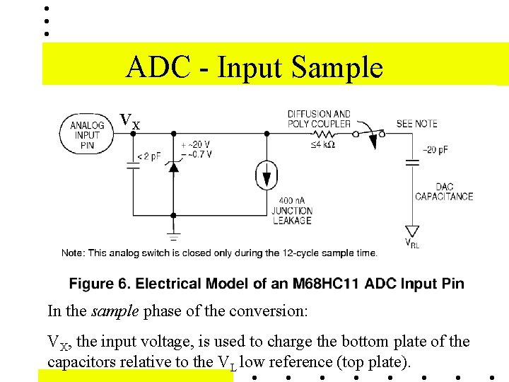
ADC - Input Sample VX In the sample phase of the conversion: VX, the input voltage, is used to charge the bottom plate of the capacitors relative to the VL low reference (top plate).
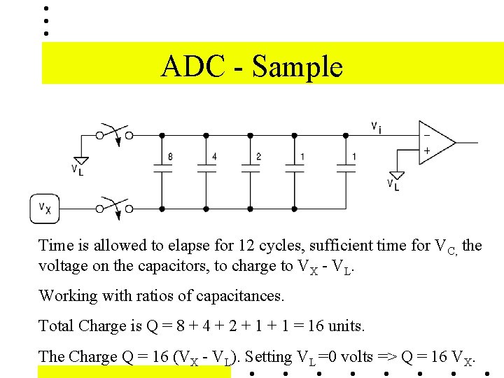
ADC - Sample Time is allowed to elapse for 12 cycles, sufficient time for VC, the voltage on the capacitors, to charge to VX - VL. Working with ratios of capacitances. Total Charge is Q = 8 + 4 + 2 + 1 = 16 units. The Charge Q = 16 (VX - VL). Setting VL =0 volts => Q = 16 VX.
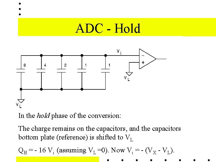
ADC - Hold In the hold phase of the conversion: The charge remains on the capacitors, and the capacitors bottom plate (reference) is shifted to VL. QH = - 16 Vi (assuming VL =0). Now Vi = - (VX - VL).
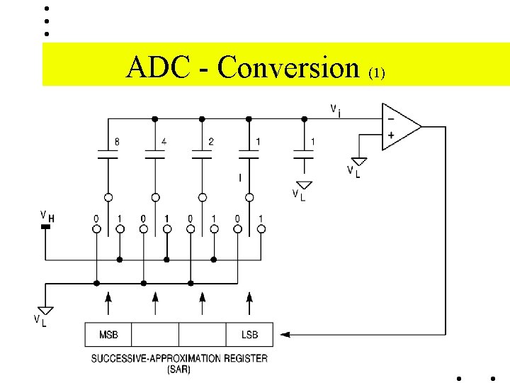
ADC - Conversion (1)
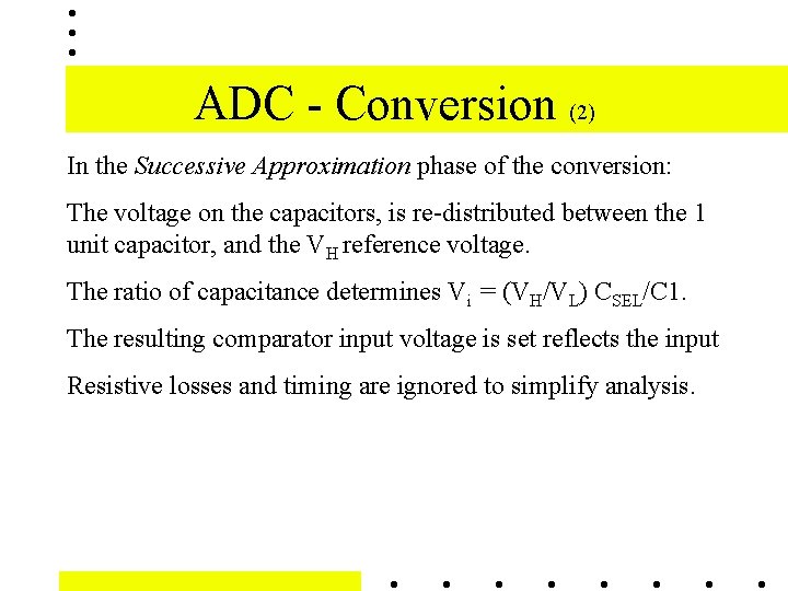
ADC - Conversion (2) In the Successive Approximation phase of the conversion: The voltage on the capacitors, is re-distributed between the 1 unit capacitor, and the VH reference voltage. The ratio of capacitance determines Vi = (VH/VL) CSEL/C 1. The resulting comparator input voltage is set reflects the input Resistive losses and timing are ignored to simplify analysis.
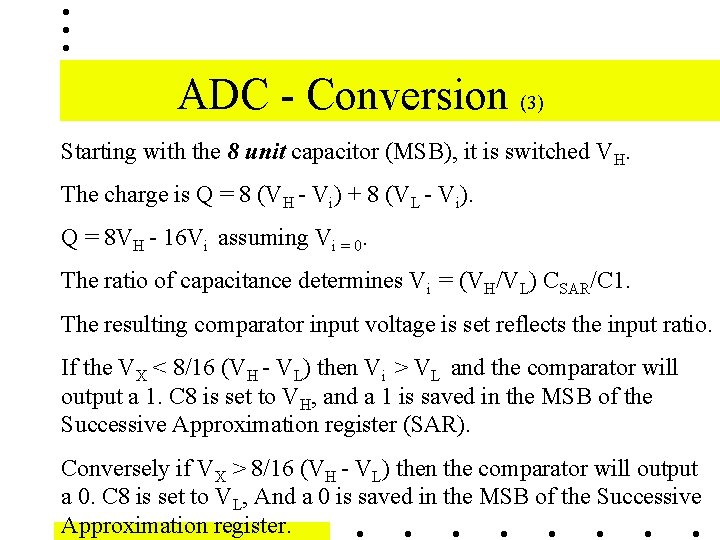
ADC - Conversion (3) Starting with the 8 unit capacitor (MSB), it is switched VH. The charge is Q = 8 (VH - Vi) + 8 (VL - Vi). Q = 8 VH - 16 Vi assuming Vi = 0. The ratio of capacitance determines Vi = (VH/VL) CSAR/C 1. The resulting comparator input voltage is set reflects the input ratio. If the VX < 8/16 (VH - VL) then Vi > VL and the comparator will output a 1. C 8 is set to VH, and a 1 is saved in the MSB of the Successive Approximation register (SAR). Conversely if VX > 8/16 (VH - VL) then the comparator will output a 0. C 8 is set to VL, And a 0 is saved in the MSB of the Successive Approximation register.
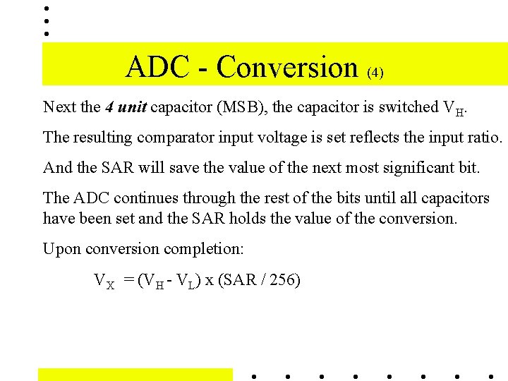
ADC - Conversion (4) Next the 4 unit capacitor (MSB), the capacitor is switched VH. The resulting comparator input voltage is set reflects the input ratio. And the SAR will save the value of the next most significant bit. The ADC continues through the rest of the bits until all capacitors have been set and the SAR holds the value of the conversion. Upon conversion completion: VX = (VH - VL) x (SAR / 256)
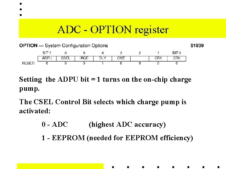
ADC - OPTION register Setting the ADPU bit = 1 turns on the on-chip charge pump. The CSEL Control Bit selects which charge pump is activated: 0 - ADC (highest ADC accuracy) 1 - EEPROM (needed for EEPROM efficiency)
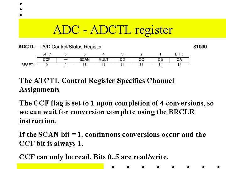
ADC - ADCTL register The ATCTL Control Register Specifies Channel Assignments The CCF flag is set to 1 upon completion of 4 conversions, so we can wait for conversion complete using the BRCLR instruction. If the SCAN bit = 1, continuous conversions occur and the CCF bit is always 1. CCF can only be read. Bits 0. . 5 are read/write.
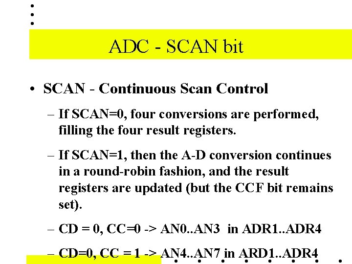
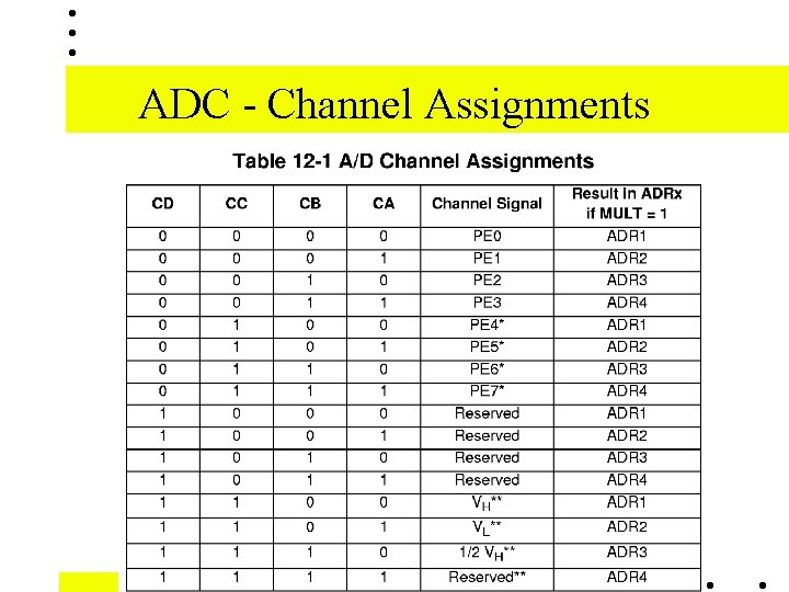
ADC - SCAN bit • SCAN - Continuous Scan Control – If SCAN=0, four conversions are performed, filling the four result registers. – If SCAN=1, then the A-D conversion continues in a round-robin fashion, and the result registers are updated (but the CCF bit remains set). – CD = 0, CC=0 -> AN 0. . AN 3 in ADR 1. . ADR 4 – CD=0, CC = 1 -> AN 4. . AN 7 in ARD 1. . ADR 4
ADC - MULT bit • MULT - Multiple Channel Control – If the MULT bit=0, then a single channel is converted and the result stored. – If MULT=1, then a conversion is performed on each channel in a group of 4 channels
ADC - Channel Assignments
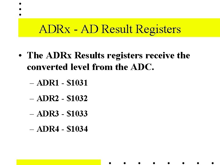
ADRx - AD Result Registers • The ADRx Results registers receive the converted level from the ADC. – ADR 1 - $1031 – ADR 2 - $1032 – ADR 3 - $1033 – ADR 4 - $1034
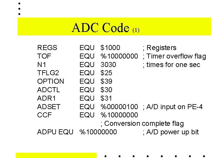
ADC Code (1) REGS TOF N 1 TFLG 2 OPTION ADCTL ADR 1 ADSET CCF EQU EQU EQU $1000 ; Registers %10000000 ; Timer overflow flag 3030 ; times for one sec $25 $39 $30 $31 %00000100 ; A/D input on PE-4 %10000000 ; Conversion complete flag ADPU EQU %10000000 ; A/D power up bit
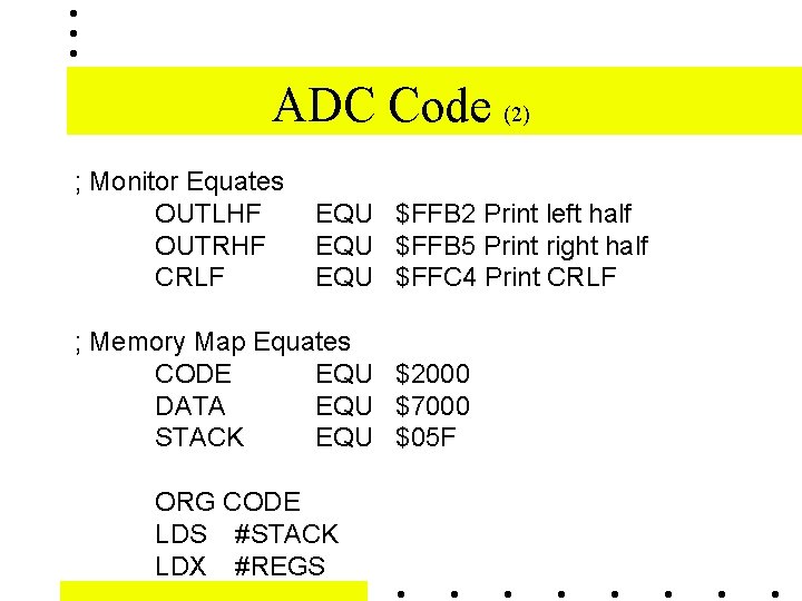
ADC Code (2) ; Monitor Equates OUTLHF OUTRHF CRLF EQU $FFB 2 Print left half EQU $FFB 5 Print right half EQU $FFC 4 Print CRLF ; Memory Map Equates CODE EQU $2000 DATA EQU $7000 STACK EQU $05 F ORG CODE LDS #STACK LDX #REGS
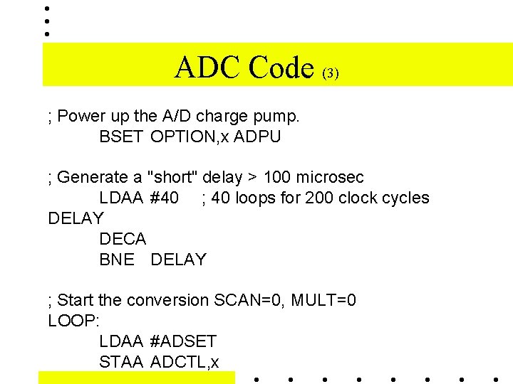
ADC Code (3) ; Power up the A/D charge pump. BSET OPTION, x ADPU ; Generate a "short" delay > 100 microsec LDAA #40 ; 40 loops for 200 clock cycles DELAY DECA BNE DELAY ; Start the conversion SCAN=0, MULT=0 LOOP: LDAA #ADSET STAA ADCTL, x
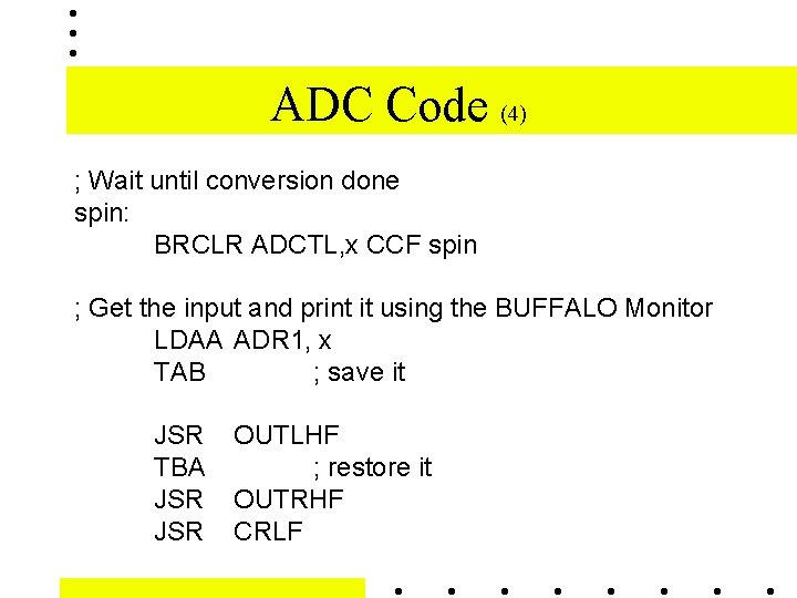
ADC Code (4) ; Wait until conversion done spin: BRCLR ADCTL, x CCF spin ; Get the input and print it using the BUFFALO Monitor LDAA ADR 1, x TAB ; save it JSR TBA JSR OUTLHF ; restore it OUTRHF CRLF
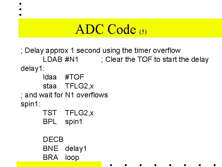
ADC Code (5) ; Delay approx 1 second using the timer overflow LDAB #N 1 ; Clear the TOF to start the delay 1: ldaa #TOF staa TFLG 2, x ; and wait for N 1 overflows spin 1: TST TFLG 2, x BPL spin 1 DECB BNE delay 1 BRA loop
Acknowledgments • Images of the configuration registers, and some source code examples, are derived from the Motorola M 68 HC 11 Reference Manual