ELE 22 MIC Lecture 12 13 Serial Communications


- Slides: 75

ELE 22 MIC Lecture 12 & 13 • • Serial Communications Serial Data Formats - RS 232 6850 ACIA HC-COM’s Serial Port - 6551 IBM PC UART: The 16550 & 16554 RS 232 / ITU V. 24 / EIA 232 Sample Interrupt Service Routine (ISR)

Serial Data Transmission (1) • Serial I/O is the transmission of data over a single communication line. – Cheaper than parallel – Data is moved sequentially one bit at a time. – Requires a conversion from parallel data format to serial format. • This conversion is normally performed by a shift register driven by a clock.

Serial Data Transmission (2) • At the receiving end, data must be reconstructed back into parallel format. • Some method is required to identify bit boundaries. • i. e. : how do you differentiate between 000 and 0000?

Serial Data Transmission (3) • Two methods: • Synchronous Transmission – Use a common clock to synchronise the receiver with the transmitter. – Therefore requires a separate tine to carry the clock. • Asynchronous Transmission – The receiver and transmitter has separate, independent, accurate local clocks.

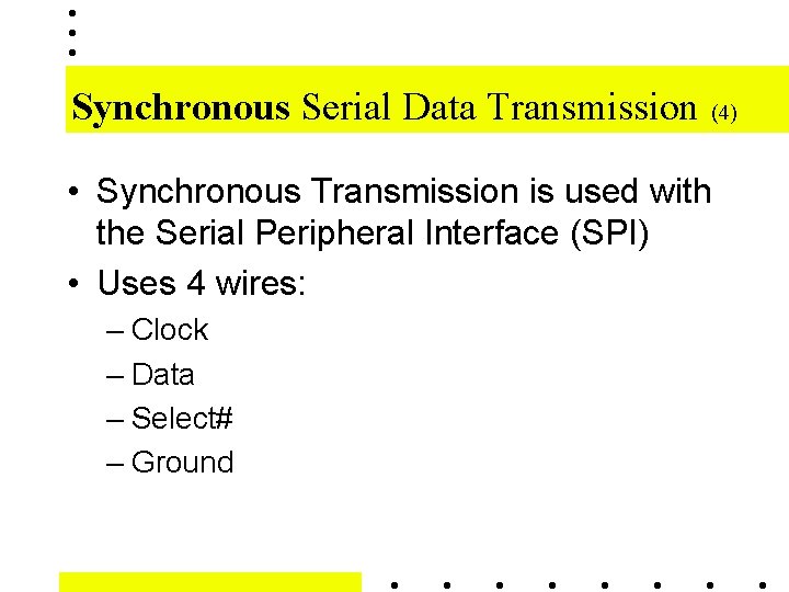
Synchronous Serial Data Transmission (4) • Synchronous Transmission is used with the Serial Peripheral Interface (SPI) • Uses 4 wires: – Clock – Data – Select# – Ground

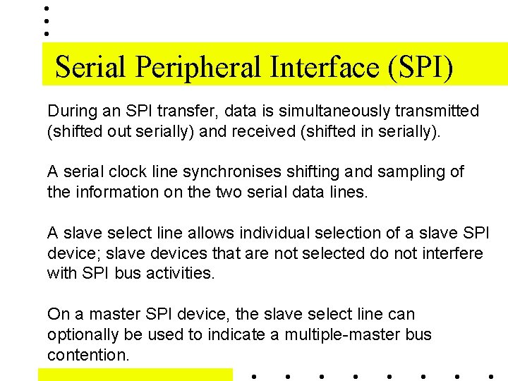
Serial Peripheral Interface (SPI) During an SPI transfer, data is simultaneously transmitted (shifted out serially) and received (shifted in serially). A serial clock line synchronises shifting and sampling of the information on the two serial data lines. A slave select line allows individual selection of a slave SPI device; slave devices that are not selected do not interfere with SPI bus activities. On a master SPI device, the slave select line can optionally be used to indicate a multiple-master bus contention.

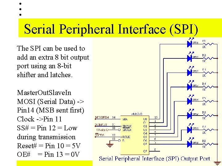
Serial Peripheral Interface (SPI) The SPI can be used to add an extra 8 bit output port using an 8 -bit shifter and latches. Master. Out. Slave. In MOSI (Serial Data) -> Pin 14 (MSB sent first) Clock ->Pin 11 SS# = Pin 12 = Low during transmission Reset# = Pin 10 = 5 V OE# = Pin 13 = 0 V

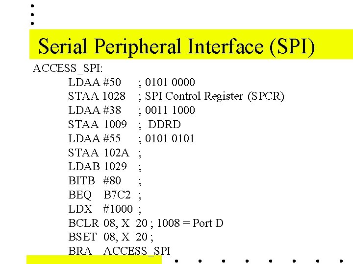
Serial Peripheral Interface (SPI) ACCESS_SPI: LDAA #50 ; 0101 0000 STAA 1028 ; SPI Control Register (SPCR) LDAA #38 ; 0011 1000 STAA 1009 ; DDRD LDAA #55 ; 0101 STAA 102 A ; LDAB 1029 ; BITB #80 ; BEQ B 7 C 2 ; LDX #1000 ; BCLR 08, X 20 ; 1008 = Port D BSET 08, X 20 ; BRA ACCESS_SPI

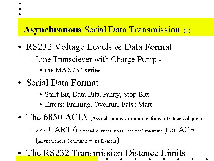
Asynchronous Serial Data Transmission (1) • RS 232 Voltage Levels & Data Format – Line Transciever with Charge Pump • the MAX 232 series. • Serial Data Format • Start Bit, Data Bits, Parity, Stop Bits • Errors: Framing, Overrun, False Start • The 6850 ACIA (Asynchronous Communications Interface Adapter) UART (Universal Asynchronous Receiver Transmitter) or ACE (Asynchronous Communications Element) – AKA: • The RS 232 Transmission Distance Limits

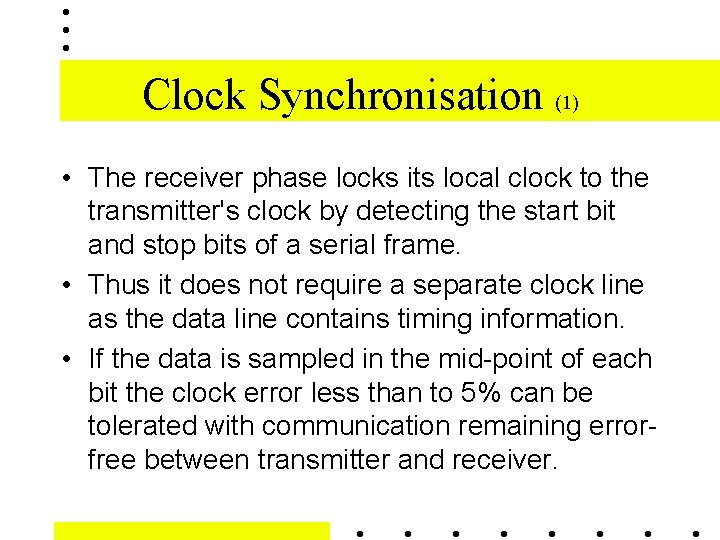
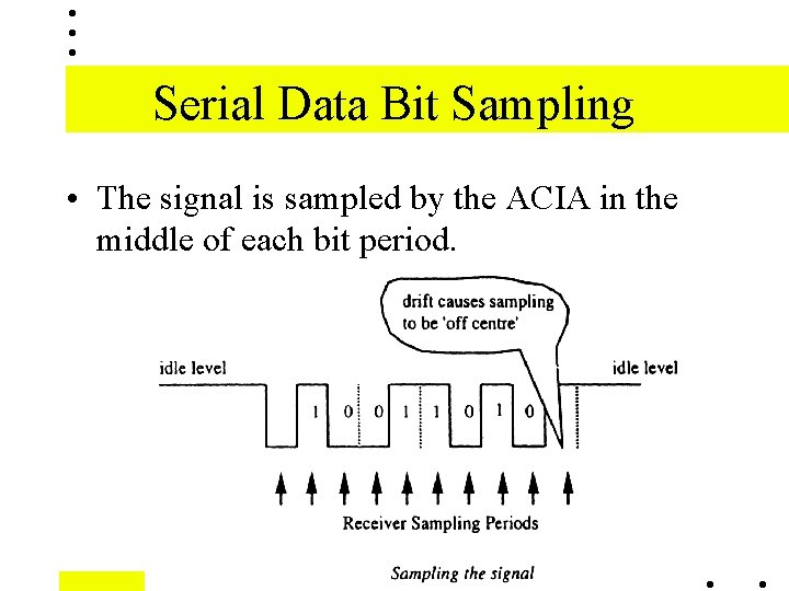
Clock Synchronisation (1) • The receiver phase locks its local clock to the transmitter's clock by detecting the start bit and stop bits of a serial frame. • Thus it does not require a separate clock line as the data line contains timing information. • If the data is sampled in the mid-point of each bit the clock error less than to 5% can be tolerated with communication remaining errorfree between transmitter and receiver.

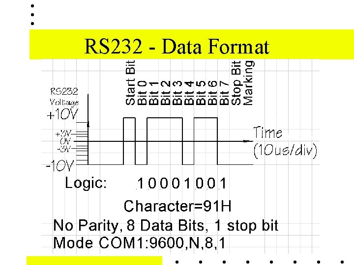
RS 232 - Data Format

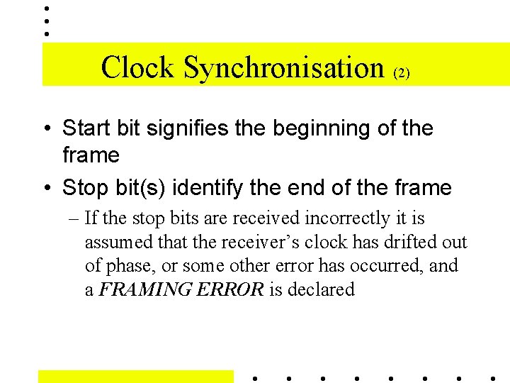
Clock Synchronisation (2) • Start bit signifies the beginning of the frame • Stop bit(s) identify the end of the frame – If the stop bits are received incorrectly it is assumed that the receiver’s clock has drifted out of phase, or some other error has occurred, and a FRAMING ERROR is declared

Serial Data Bit Sampling • The signal is sampled by the ACIA in the middle of each bit period.

Serial Communication Speed • The rate at which data is transmitted is called the bit-rate • Bit-rate is measured in bits per second. • Baud rate refers to the rate per second of the bit symbols used to transmit the serial data. • i. e. : it includes the synchronisation items: start bit & stop bit(s). For example: If using 10 bit symbols per 8 bit character at 9600 baud equates to a bit rate of 7680 data bits per second (or 960 Bytes per second).

Serial Data Bit Error Detection • In any data transfer there is the potential for bit-errors. Parity can be used as a check that the correct bit pattern is received. • Parity calculation involves adding the “ 1” bits in a frame together. • Even Parity – Adding all bits in frame + parity => ‘ 0’ • Odd Parity – Adding all bits in frame + parity => ‘ 1’

Serial Data Bit Error Detection

Bit Error Rate (BER) (1) • The Bit Error Rate - Probability of bit error - is the number of bit errors measured at the receiver through a communication system. The transmission channel may be Radio, Optical Fibre, Copper Cable, etc. • In analog communications the important unit of measure is the Signal to Noise ratio. • These measures are useful to characterise a system and can be measured or simulated.

Bit Error Rate (BER) (2) • If the quality of the system is high, the single bit error rate may be measured in years. In this case a single parity bit would be sufficient to determine data errors & retransmission could recover the correct data. • The probability of double-bit errors would become negligable. Double-bit errors cannot be detected using a single parity bit.

Improving Noise Immunity • One way of improving noise immunity: sample multiple times through each bit and at each sample time, check the status of each bit. Take the most common value of the sample as the bit value.

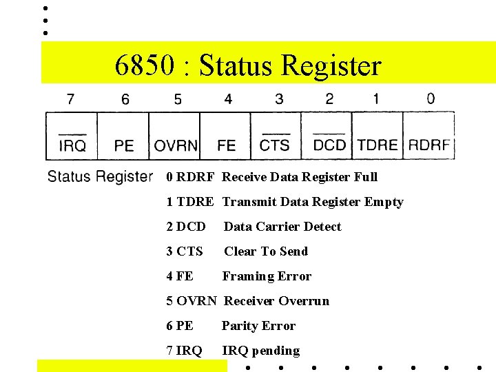
6850 : Status Register 0 RDRF Receive Data Register Full 1 TDRE Transmit Data Register Empty 2 DCD Data Carrier Detect 3 CTS Clear To Send 4 FE Framing Error 5 OVRN Receiver Overrun 6 PE Parity Error 7 IRQ pending

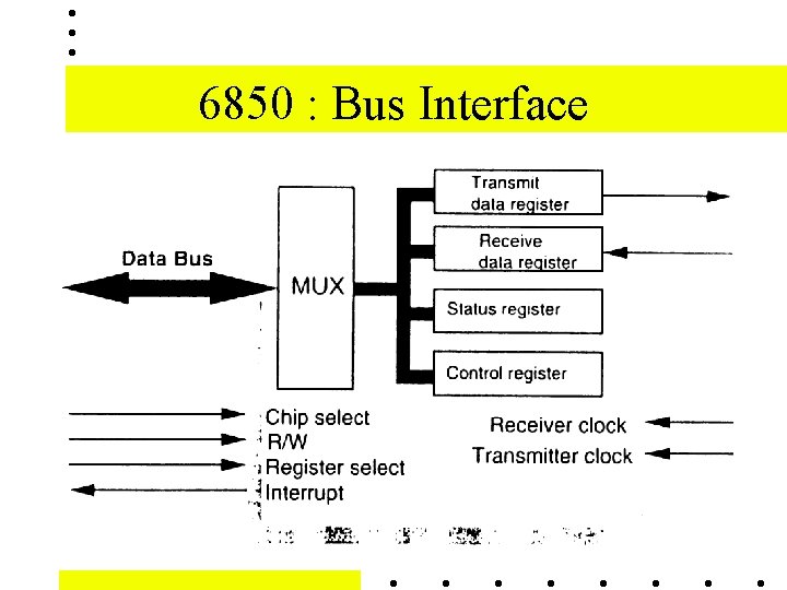
6850 : Bus Interface

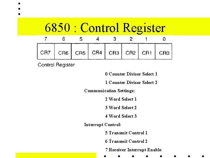
6850 : Control Register Clock divisor: 0 Counter Divisor Select 1 1 Counter Divisor Select 2 Communication Settings: 2 Word Select 1 3 Word Select 2 4 Word Select 3 Interrupt Control: 5 Transmit Control 1 6 Transmit Control 2 7 Receiver Interrupt Enable

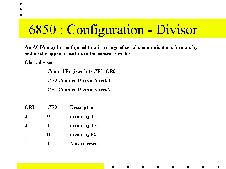
6850 : Configuration - Divisor An ACIA may be configured to suit a range of serial communications formats by setting the appropriate bits in the control register Clock divisor: Control Register bits CR 1, CR 0 Counter Divisor Select 1 CR 1 Counter Divisor Select 2 CR 1 CR 0 Description 0 0 divide by 1 0 1 divide by 16 1 0 divide by 64 1 1 Master reset

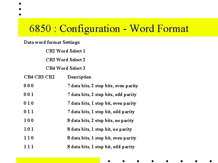
6850 : Configuration - Word Format Data word format Settings: CR 2 Word Select 1 CR 3 Word Select 2 CR 4 Word Select 3 CR 4 CR 3 CR 2 Description 000 7 data bits, 2 stop bits, even parity 001 7 data bits, 2 stop bits, odd parity 010 7 data bits, 1 stop bit, even parity 011 7 data bits, 1 stop bit, odd parity 100 8 data bits, 2 stop bits, no parity 101 8 data bits, 1 stop bit, no parity 110 8 data bits, 1 stop bit, even parity 111 8 data bits, 1 stop bit, odd parity

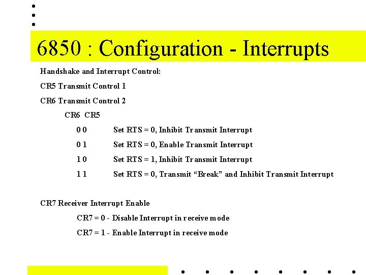
6850 : Configuration - Interrupts Handshake and Interrupt Control: CR 5 Transmit Control 1 CR 6 Transmit Control 2 CR 6 CR 5 00 Set RTS = 0, Inhibit Transmit Interrupt 01 Set RTS = 0, Enable Transmit Interrupt 10 Set RTS = 1, Inhibit Transmit Interrupt 11 Set RTS = 0, Transmit “Break” and Inhibit Transmit Interrupt CR 7 Receiver Interrupt Enable CR 7 = 0 - Disable Interrupt in receive mode CR 7 = 1 - Enable Interrupt in receive mode

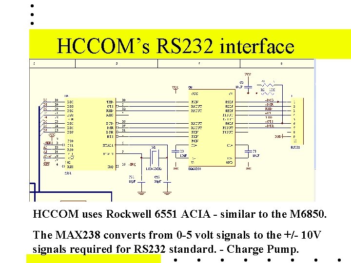
HCCOM’s RS 232 interface HCCOM uses Rockwell 6551 ACIA - similar to the M 6850. The MAX 238 converts from 0 -5 volt signals to the +/- 10 V signals required for RS 232 standard. - Charge Pump.

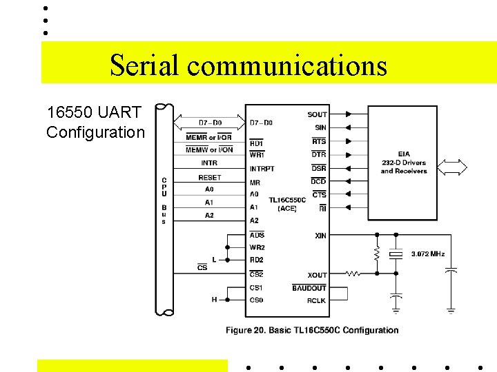
Serial communications 16550 UART Configuration

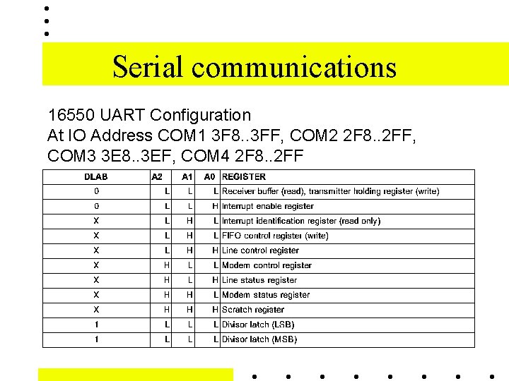
Serial communications 16550 UART Configuration At IO Address COM 1 3 F 8. . 3 FF, COM 2 2 F 8. . 2 FF, COM 3 3 E 8. . 3 EF, COM 4 2 F 8. . 2 FF


Serial communications Interrupt Enable Register (IER) The IER enables each of the five types of interrupts and enables INTRPT in response to an interrupt generation. The IER can also disable the interrupt system by clearing bits 0 through 3. The contents of this register are summarised in the previous table

Serial communications Interrupt Identification Register (IIR) P 1 The ACE has an on-chip interrupt generation and prioritization capability. The ACE provides four prioritized levels of interrupts: Priority 1 - Receiver line status (highest priority) Priority 2 - Receiver data ready/receiver character time-out Priority 3 - Transmitter holding register empty Priority 4 - Modem status (lowest priority) When an interrupt is generated, the IIR indicates that an interrupt is pending and encodes the type of interrupt in its three least significant bits (bits 0, 1, and 2).

Serial communications Interrupt Identification Register (IIR) P 2 Detail on each bit is as follows: Bit 0: When bit 0 is cleared, an interrupt is pending Bits 1 and 2: These two bits identify the highest priority interrupt pending as indicated in the previous table. Bit 3: This bit is always cleared in 16 C 450 mode. In FIFO mode, bit 3 is set with bit 2 to indicate that a time-out interrupt is pending. Bits 4 and 5: not used (always cleared). Bits 6 and 7: These bits are always cleared in 16 C 450 mode. They are set when bit 0 of the FIFO control register is set.

Serial communications Line Control Register (LCR) In addition, the programmer is able to retrieve, inspect, and modify the contents of the LCR; this eliminates the need for separate storage of the line characteristics in system memory. Bits 0 and 1: Number of bits in each serial character. 00=5 bits, 01=6 bits, 10=7 bits, 11=8 bits Bit 2: Specifies either 1, 1. 5 or 2 stop bits If Bit 3=: parity bit is generated in transmitted data between the last data word bit and the first stop bit. In received data parity is checked. If Bit 3=0: no parity is generated or checked.

Serial communications Line Control Register (LCR) When parity is enabled and: Bit 4=1 Even Parity - An even number of logic 1 s in the data and parity bits is selected. Bit 4=0 odd parity - An odd number of logic 1 s is selected. Bit 5=1 Stick Parity. The parity bit set to 0. Bit 5=0 Stick parity is disabled.

Serial communications Line Control Register (LCR) Bit 6: Break control bit. Bit 6 is set to force a break condition; i. e. , a condition where SOUT is forced to the spacing (cleared) state. Bit 7: Divisor Latch Access Bit (DLAB). Bit 7 must be set to access the divisor latches of the baud generator during a read or write. Bit 7 must be cleared during a read or write to access the receiver buffer, the THR, or the IER.

Serial communications Line Status Register (LSR) Bit 0: Data Ready (DR) indicator for the receiver. DR is set whenever a complete incoming character has been received and transferred into the RBR or the FIFO. DR is cleared by reading all of the data in the RBR or the FIFO. Bit 1 : Overrun Error (OE) indicator. When OE is set, it indicates that before the character in the RBR was read, it was overwritten by the next character transferred into the register.

Serial communications Line Status Register (LSR) Bit 2: Parity Error (PE) indicator. When PE is set, it indicates that the parity of the received data character does not match the parity selected. In the FIFO mode, this error is associated with the particular character in the FIFO to which it applies. This error is revealed to the CPU when its associated character is at the top of the FIFO. Bit 3: Framing Error (FE) indicator. When FE is set, it indicates that the received character did not have a valid (set) stop bit. Bit 4: Break Interrupt (BI) indicator. When BI is set, it indicates that the received data input was held low for longer than a full-word transmission time.

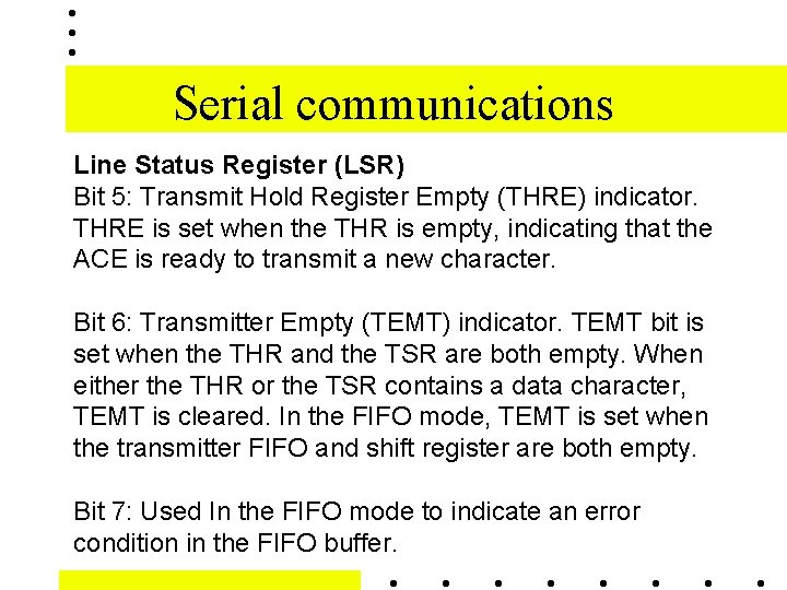
Serial communications Line Status Register (LSR) Bit 5: Transmit Hold Register Empty (THRE) indicator. THRE is set when the THR is empty, indicating that the ACE is ready to transmit a new character. Bit 6: Transmitter Empty (TEMT) indicator. TEMT bit is set when the THR and the TSR are both empty. When either the THR or the TSR contains a data character, TEMT is cleared. In the FIFO mode, TEMT is set when the transmitter FIFO and shift register are both empty. Bit 7: Used In the FIFO mode to indicate an error condition in the FIFO buffer.

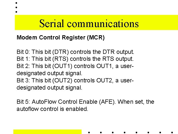
Serial communications Modem Control Register (MCR) Bit 0: This bit (DTR) controls the DTR output. Bit 1: This bit (RTS) controls the RTS output. Bit 2: This bit (OUT 1) controls OUT 1, a userdesignated output signal. Bit 3: This bit (OUT 2) controls OUT 2, a userdesignated output signal. Bit 5: Auto. Flow Control Enable (AFE). When set, the autoflow control is enabled.

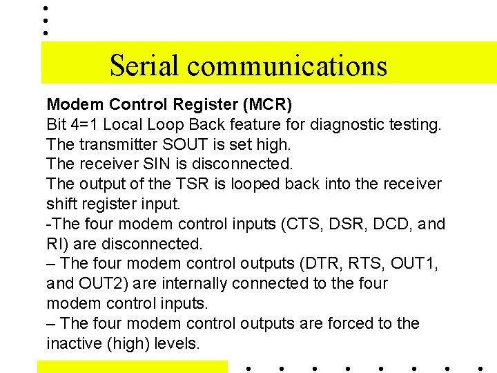
Serial communications Modem Control Register (MCR) Bit 4=1 Local Loop Back feature for diagnostic testing. The transmitter SOUT is set high. The receiver SIN is disconnected. The output of the TSR is looped back into the receiver shift register input. -The four modem control inputs (CTS, DSR, DCD, and RI) are disconnected. – The four modem control outputs (DTR, RTS, OUT 1, and OUT 2) are internally connected to the four modem control inputs. – The four modem control outputs are forced to the inactive (high) levels.

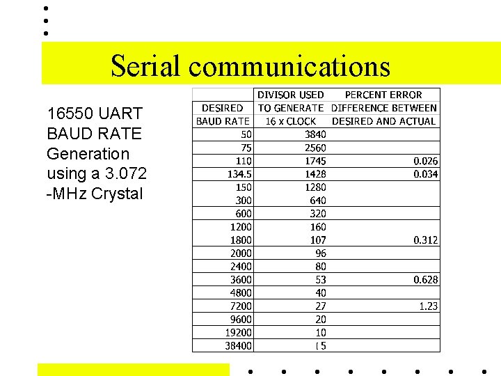
Serial communications 16550 UART BAUD RATE Generation using a 3. 072 -MHz Crystal

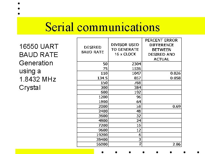
Serial communications 16550 UART BAUD RATE Generation using a 1. 8432 MHz Crystal

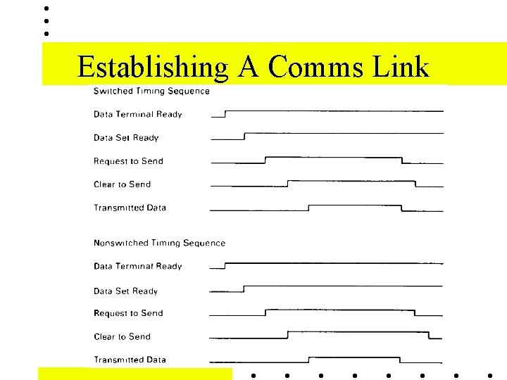
Establishing A Comms Link

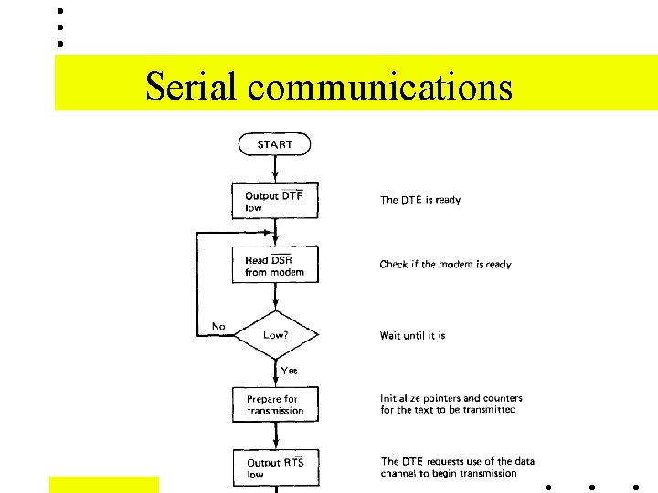
Serial communications

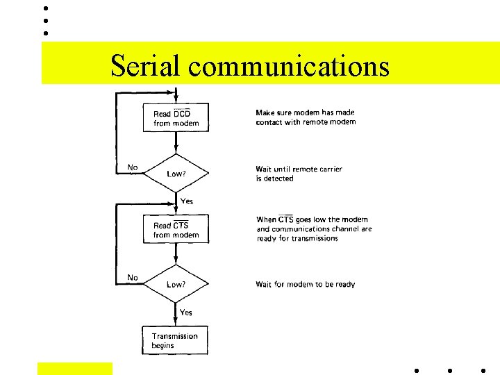
Serial communications

Modern Serial communications The 16 C 550 x are functional upgrades of the 16 C 450 - equivalent to the 16 C 450 on power up, but can be placed in an alternate FIFO mode. The automatic FIFO mode relieves the CPU of excessive software overhead by buffering received and transmitted characters. The receiver and transmitter FIFOs store up to 16 bytes including three additional bits of error status per byte for the receiver FIFO.

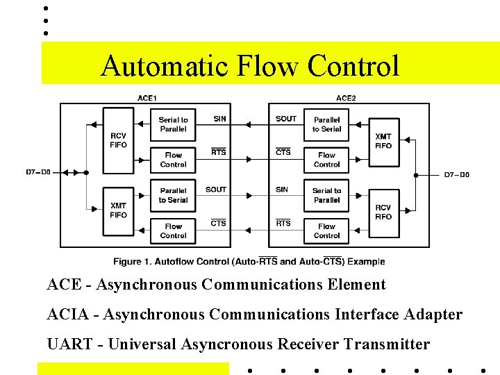
Modern Serial communications In the FIFO mode, there is a selectable autoflow control feature that can significantly reduce software overload and increase system efficiency by automatically controlling serial data flow using RTS output and CTS input signals.

Automatic Flow Control ACE - Asynchronous Communications Element ACIA - Asynchronous Communications Interface Adapter UART - Universal Asyncronous Receiver Transmitter

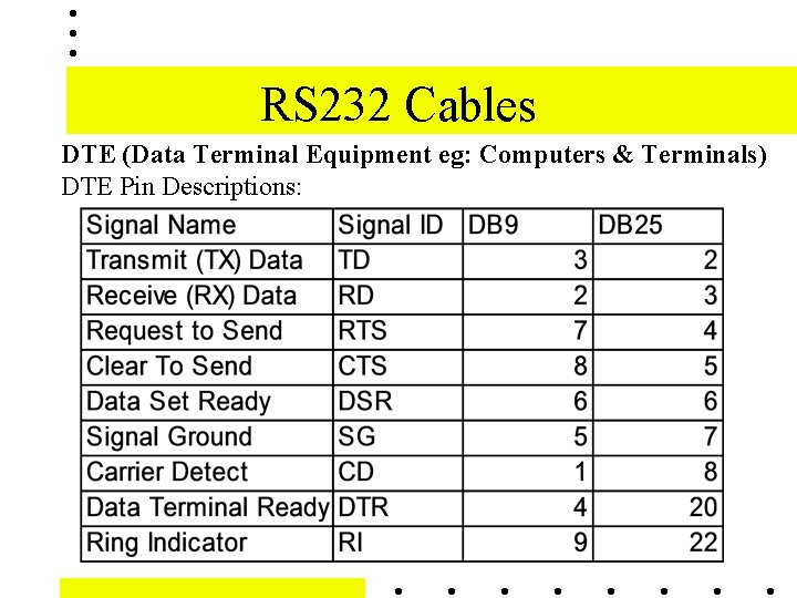
RS 232 Cables DTE (Data Terminal Equipment eg: Computers & Terminals) DTE Pin Descriptions:

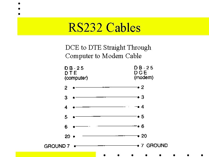
RS 232 Cables DCE to DTE Straight Through Computer to Modem Cable

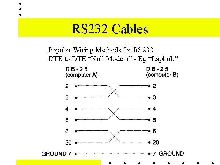
RS 232 Cables Popular Wiring Methods for RS 232 DTE to DTE “Null Modem” - Eg “Laplink”

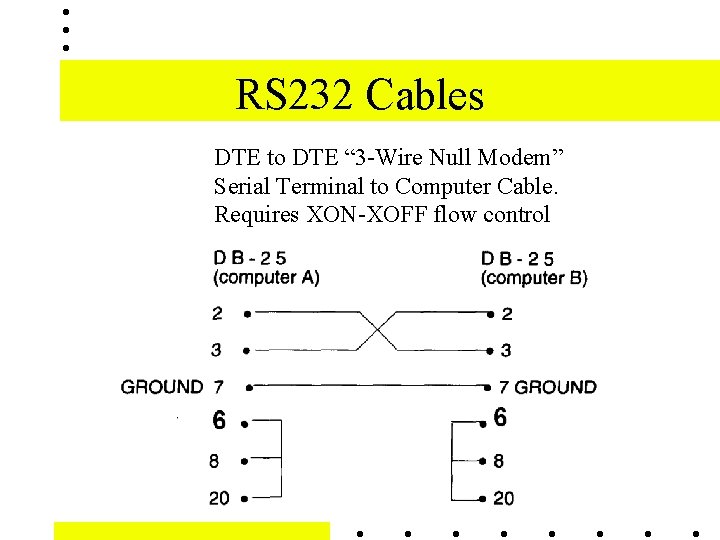
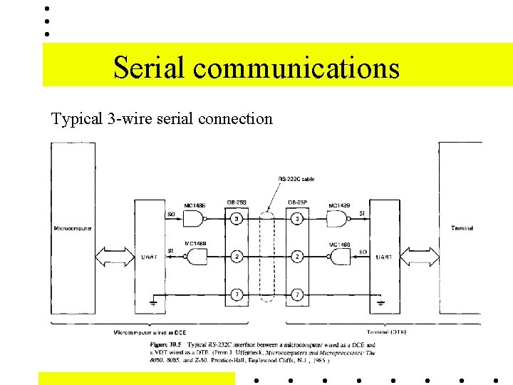
RS 232 Cables DTE to DTE “ 3 -Wire Null Modem” Serial Terminal to Computer Cable. Requires XON-XOFF flow control

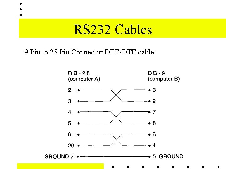
RS 232 Cables 9 Pin to 25 Pin Connector DTE-DTE cable

Serial communications Typical 3 -wire serial connection

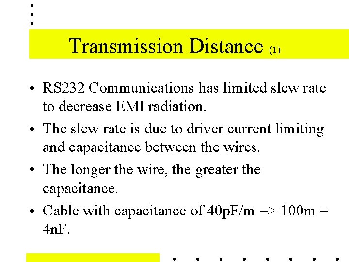
Transmission Distance (1) • RS 232 Communications has limited slew rate to decrease EMI radiation. • The slew rate is due to driver current limiting and capacitance between the wires. • The longer the wire, the greater the capacitance. • Cable with capacitance of 40 p. F/m => 100 m = 4 n. F.

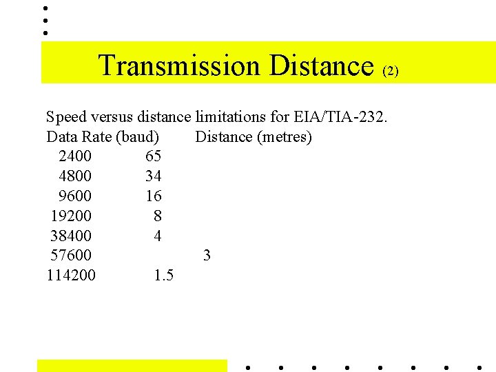
Transmission Distance (2) Speed versus distance limitations for EIA/TIA-232. Data Rate (baud) Distance (metres) 2400 65 4800 34 9600 16 19200 8 38400 4 57600 3 114200 1. 5

Interrupts (1) There are two ways of telling when an I/O device is ready: 1. polling 2. interrupts An interrupt is a way of diverting the processor's attention away from its current program so that it may deal with some event that has occurred. change in state of a peripheral error from a peripheral Using interrupts means the processor does not have to continuously poll (check) the status of I/O devices.

Interrupts (2) In some processors, an interrupt is also known as a TRAP. In other cases TRAPs refer to system-generated interrupts for example: errors such as : division by 0, invalid opcode, access invalid memory address There are two types of interrupt • hardware • software A hardware interrupt may be thought of as a hardwaregenerated call to a special subroutine.

Interrupts (3) The 68 HC 11 has three direct hardware interrupts. 1. IRQ saves the state of the processor - loads the IRQ vector - executes the IRQ ISR - restores the state of the processor - orginal program in resumed. IRQ is maskable 2. XIRQ high priority interrupt - non-maskable 3. RESET - RESET line is held low for 8 cycles, loads RESET vector, computer restarts and previous CPU state is lost. RESET used on power-up or after catastrophic hardware or software failure non-maskable (highest priority). Some processors have special interrupts known as fast interrupts. (They are fast as they don’t save the cpu state, but leave that to the ISR writer’s discretion)

Interrupts (4) When a processor receives an interrupt, it: completes its current instruction masks further interrupts saves it current state loads address of routine to handle interrupt executes Interrupt Service Routine (ISR) to exit the ISR: Returns from interrupt using RTI instruction which restores the previous state

Interrupts (5) Upon IRQ interrupt: current instruction completes, if interrupts are not masked: the interrupt mask is set, then the 68 HC 11 saves on the stack: program counter Y index register X index register accumulator A accumulator B CCR Upon returning from any interrupt - uses the RTI instruction the 68 HC 11 pulls (pops) back from the stack: CCR accumulator B accumulator A X index register Y index register program counter

Interrupts (6) The Interrupt Service Routine (ISR) is a subroutine specifically designed to handle a given interrupt. An ISR is run when the processor receives an interrupt. The CPU loads the vector corresponding to that interrupt that points to the appropriate ISR. Each interrupt usually has a separate ISR associated with it. An ISR will then - determine the source of the interrupt - deal with event appropriately - Return from Interrupt (execute an RTI instruction)

Interrupts (7) Interrupts may be handled in two ways Interrupt polling: - ISR checks each device to find the device that generated the interrupt - used when processor has limited number of interrupt lines (wired-OR IRQ#) - used when I/O device has several sources of interrupt Vectored interrupts: - each device corresponds to a single interrupt line and therefore a single vector or - an I/O operation will supply the processor with a vector appropriate for the event that has occurred

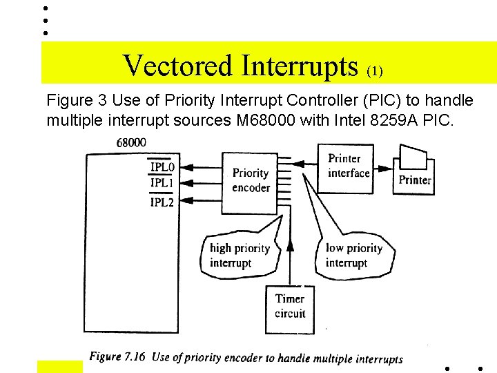
Vectored Interrupts (1) Figure 3 Use of Priority Interrupt Controller (PIC) to handle multiple interrupt sources M 68000 with Intel 8259 A PIC.

Software Interrupts (1) The 68 HC 11 has just one software interrupt (swi). It is used to Call BUFFALO on HCCOM. On 80 x 86 systems the software interrupt is used by programs to request services from the operating system. ROM BIOS / DOS. eg: Print this character Read a string of characters Read from the disk xxxx bytes to memory yyyy Check for network errors Request for termination How software interrupts are implemented depends on the operating system.

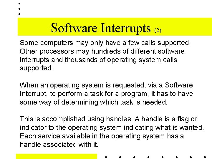
Software Interrupts (2) Some computers may only have a few calls supported. Other processors may hundreds of different software interrupts and thousands of operating system calls supported. When an operating system is requested, via a Software Interrupt, to perform a task for a program, it has to have some way of determining which task is needed. This is accomplished using handles. A handle is a flag or indicator to the operating system indicating what is wanted. Each service available in the operating system has a handle associated with it.

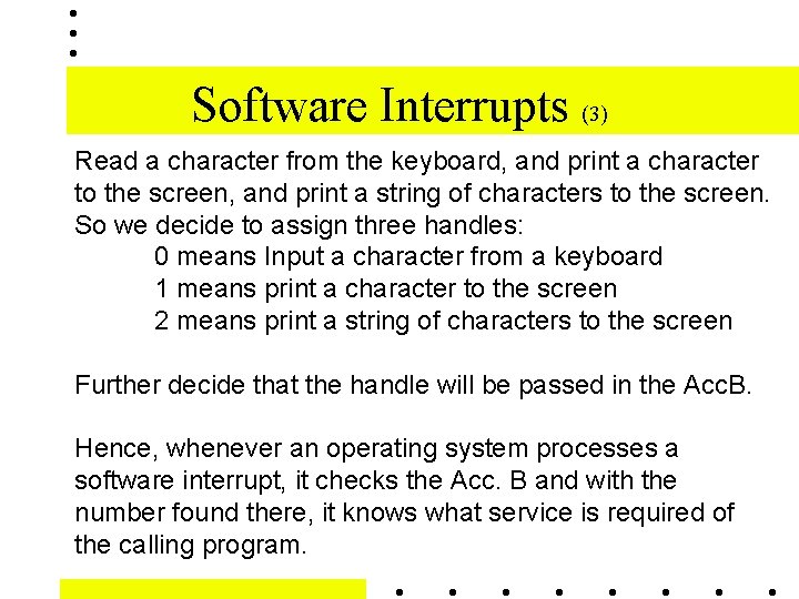
Software Interrupts (3) Read a character from the keyboard, and print a character to the screen, and print a string of characters to the screen. So we decide to assign three handles: 0 means Input a character from a keyboard 1 means print a character to the screen 2 means print a string of characters to the screen Further decide that the handle will be passed in the Acc. B. Hence, whenever an operating system processes a software interrupt, it checks the Acc. B and with the number found there, it knows what service is required of the calling program.

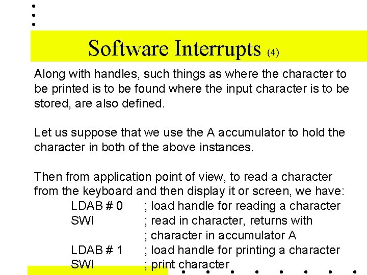
Software Interrupts (4) Along with handles, such things as where the character to be printed is to be found where the input character is to be stored, are also defined. Let us suppose that we use the A accumulator to hold the character in both of the above instances. Then from application point of view, to read a character from the keyboard and then display it or screen, we have: LDAB # 0 ; load handle for reading a character SWI ; read in character, returns with ; character in accumulator A LDAB # 1 ; load handle for printing a character SWI ; print character

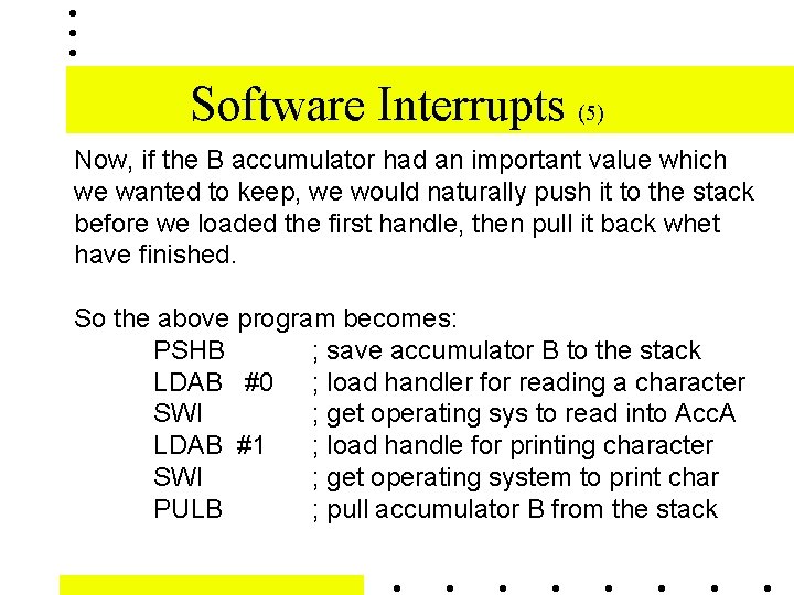
Software Interrupts (5) Now, if the B accumulator had an important value which we wanted to keep, we would naturally push it to the stack before we loaded the first handle, then pull it back whet have finished. So the above program becomes: PSHB ; save accumulator B to the stack LDAB #0 ; load handler for reading a character SWI ; get operating sys to read into Acc. A LDAB #1 ; load handle for printing character SWI ; get operating system to print char PULB ; pull accumulator B from the stack

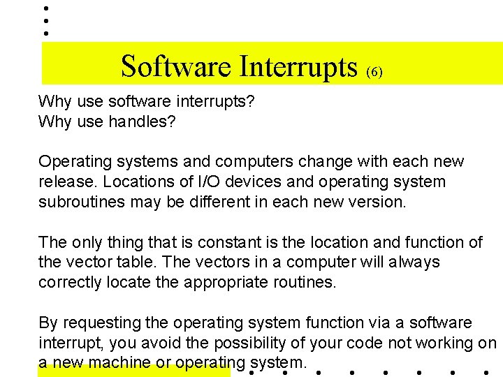
Software Interrupts (6) Why use software interrupts? Why use handles? Operating systems and computers change with each new release. Locations of I/O devices and operating system subroutines may be different in each new version. The only thing that is constant is the location and function of the vector table. The vectors in a computer will always correctly locate the appropriate routines. By requesting the operating system function via a software interrupt, you avoid the possibility of your code not working on a new machine or operating system.

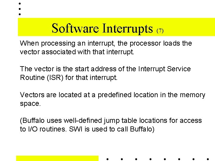
Software Interrupts (7) When processing an interrupt, the processor loads the vector associated with that interrupt. The vector is the start address of the Interrupt Service Routine (ISR) for that interrupt. Vectors are located at a predefined location in the memory space. (Buffalo uses well-defined jump table locations for access to I/O routines. SWI is used to call Buffalo)

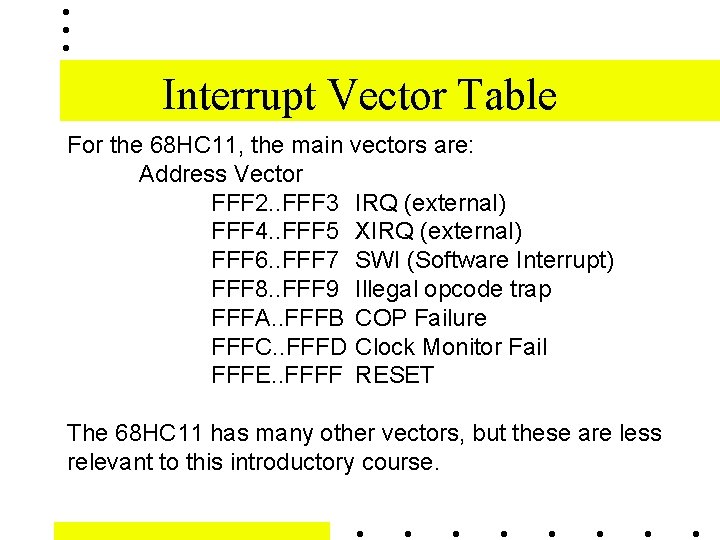
Interrupt Vector Table For the 68 HC 11, the main vectors are: Address Vector FFF 2. . FFF 3 IRQ (external) FFF 4. . FFF 5 XIRQ (external) FFF 6. . FFF 7 SWI (Software Interrupt) FFF 8. . FFF 9 Illegal opcode trap FFFA. . FFFB COP Failure FFFC. . FFFD Clock Monitor Fail FFFE. . FFFF RESET The 68 HC 11 has many other vectors, but these are less relevant to this introductory course.

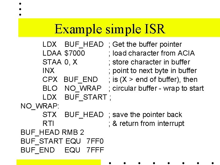
Example simple ISR LDX BUF_HEAD ; Get the buffer pointer LDAA $7000 ; load character from ACIA STAA 0, X ; store character in buffer INX ; point to next byte in buffer CPX BUF_END ; is (X > end of buffer), then BLO NO_WRAP ; circular buffer - wrap to start LDX BUF_START ; NO_WRAP: STX BUF_HEAD ; save the pointer back RTI ; & return from interrupt BUF_HEAD RMB 2 BUF_START EQU 7 FF 0 BUF_END EQU 7 FFF

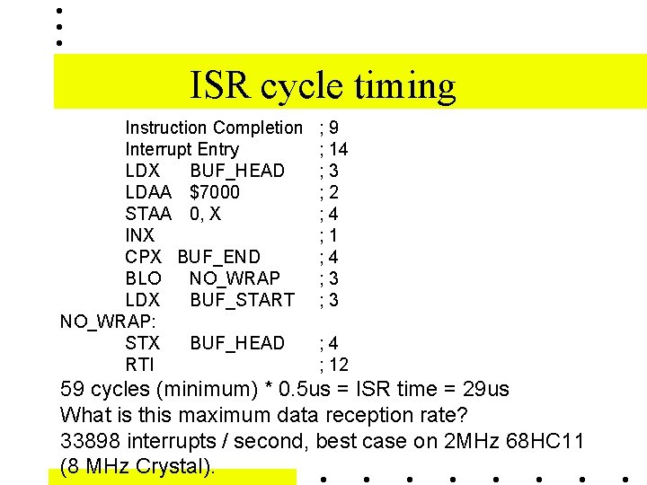
ISR cycle timing Instruction Completion Interrupt Entry LDX BUF_HEAD LDAA $7000 STAA 0, X INX CPX BUF_END BLO NO_WRAP LDX BUF_START NO_WRAP: STX BUF_HEAD RTI ; 9 ; 14 ; 3 ; 2 ; 4 ; 1 ; 4 ; 3 ; 4 ; 12 59 cycles (minimum) * 0. 5 us = ISR time = 29 us What is this maximum data reception rate? 33898 interrupts / second, best case on 2 MHz 68 HC 11 (8 MHz Crystal).

Acknowledgements • I used Altium Protel 98 and Protel DXP to create these schematic diagrams • Motorola 11 rm. pdf Reference Manual • IEEE Electronics Engineers’ Handbook, 4 th Edn, Donald Christiansen - Definitions of BAUD & BER • Seng Goh’s original notes