ELE 2 MIC Lecture 19 MULTIPLEXOR DATA SELECTOR

 many inputs to one output • Switch")
 | (Input 1 & Select)")


")
 Erasure of Cells is performed by providing a tunnelling voltage to")
 Programming of Cells is performed by providing a tunnelling voltage to")
")
")
")
.")


- Slides: 36
ELE 2 MIC Lecture 19 • • • MULTIPLEXOR - DATA SELECTOR DEMULTIPLEXOR - DATA DISTRIBUTOR External Address Bus Timing Diagrams Address Decoding using a 74 LS 138
Multiplexor - Data Selector • Multiplex (MUX) many inputs to one output • Switch selects the one signal source from many input signals. • Like Stereo Hi. Fi source selection switch
Two Input Multiplexor Output = (Input 0 & Select#) | (Input 1 & Select)
Four Input Multiplexor
Eight Input Multiplexor
74 F 151 8 -Input MUX
74 F 151 8 -Input MUX Pin Names and Loading / Fanout
Mux vs De. Mux
AVR On-Chip SRAM Timing
AVR Data Ram • When 4 KB is enough RAM for an application, the On-Chip SRAM is sufficient. • When 4 KB is insufficient, an external RAM chip can be used to expand the address range to 64 K bytes. • There are four memory configuration options for external RAM.
AVR External Data Ram • By setting the XMEM bit to 1, the e. Xternal MEMory interface is enabled, and the dedicated external memory control lines become active. • The dedicated controls are ALE#, RE#, WE# and the multiplexed address & data bus bits 0. . 7 and the address bits 8. . 15 take control, overriding the port A, port C and port G (pins 0. . 2) functions.
AVR External Data Ram • The dedicated control signals are: • RE# - Read Enable - Active Low – Data is read from the external memory (or device) into the AVR microcontroller. • WE# - Write Enable - Active Low – Data is written from the AVR to the external memory (or device).
AVR External Data Ram • ALE - Address Latch Enable - Active High. • When ALE transitions high, the Memory Address Register is asserted onto the Multiplexed Address & Data bus lines • the bus enters a write-address phase • the address is latched into an external address latch which is used to form an system’s external address bus.
AVR External Data Ram • ALE - Address Latch Enable - Active High. • When ALE is low, a data phase commences and data can be read or written to the external memory or device. • (external in this context refers to off-chip memory)
AVR External Address Latch
AVR External Mem Timing
AVR External Mem Timing
68 HC 11 External Address Latch
HC 11 Strobe Timing Diagram
Applications of a de-multiplexor • The Memory Chip Select device used on the original IBM PC is a 74 xx 138 de-multiplexor. • The 74 LS 138 is used to activate 1 of 8 lines based on the conditions of the three binary select inputs A, B & C, and the three enable inputs. • The 74 LS 138 Outputs are “Active Low”.
74 LS 138 8 -Output DEMUX De-Multiplex one input to many outputs -Reverse operation of a multiplexor 74 LS 138 Truth Table
De. Multiplexor • The 74 LS 138 can be implemented by the logic shown. • The 54 LS 138 is identical in function, but can operate over the “Mil-spec” -55°C to 125°C Temperature Range. • The 74 LS 138 can operate over the Commercial 0°C 70°C Temperature Range.
Memory Select
Address Decoding & Chip Select • • A 15 -> G 1#, E -> G, A 14 -> A 2, A 13 -> A 1 R/W# -> A 0 Chip is enabled when A 15 = 0 & E is High Y 2 = (A 14#) & (A 13) & Write (R/W#=0) & E Y 3 = (A 14#) & (A 13) & Read (R/W#=1) & E Y 4 = (A 14) & (A 13#) & Write (R/W#=0) & E Y 5 = (A 14) & (A 13#) & Read (R/W#=1) & E
Write Data Timing Diagram
EEPROM Technology (1)
EEPROM Technology (2) Erasure of Cells is performed by providing a tunnelling voltage to the control gate which causes the charge on the floating gate to be removed. When read, each cell returns a logical ‘ 1’ value.
EEPROM Technology (3) Programming of Cells is performed by providing a tunnelling voltage to the control gate which causes the charge to be placed on the floating gate. The write process writes the ‘ 0’s into each cell.
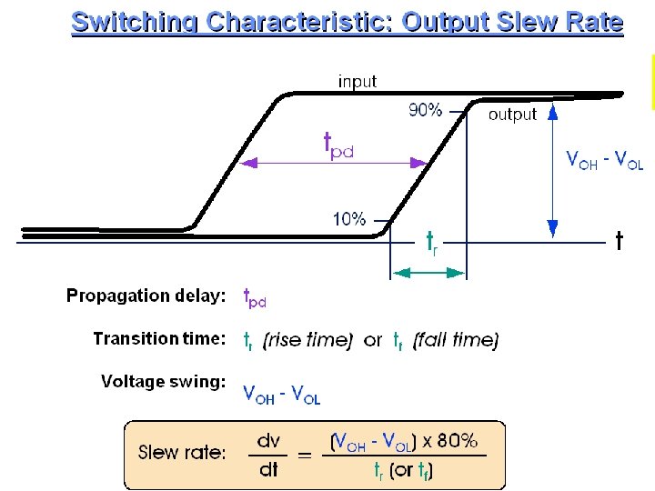
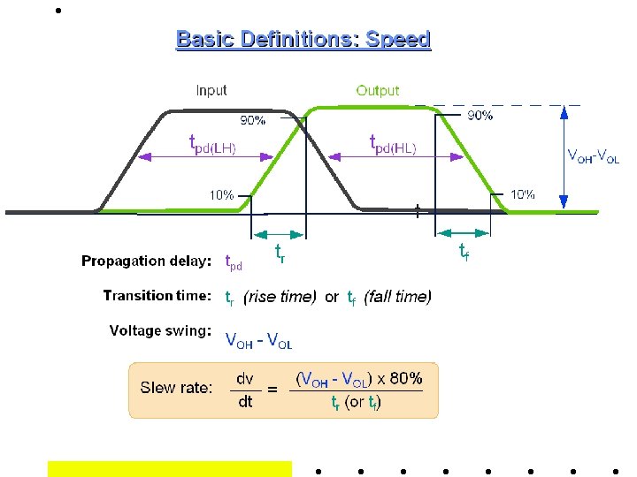
Logic Family - Propagation Delay (H-L)
Logic Family - Propagation Delay (L-H)
Logic Family - Propagation Delay (3)
Bus Design Rules Bus lines have very low line impedances (20. . 40 Ohms). • Bus lines have to be terminated to prevent line reflections (signal distortion, circuit malfunctions due to undershoots). • Take care of propagation times (25 ns/m). Settling time of signals on TTL-type buses is 2 x tp (no incident wave switching). • Take care of control lines (clock, read, write, etc. ). • Provide shielding between control lines and data / address lines.
Bus Design Rules • A multiplexed data and address bus reduces design problems (50% less signal lines and 50% less line drivers). • Driver output current is 100 m. A/line. Provide adequate and low inductance GND return path (simultaneous switching)! • Rule of thumb: 25% of all backplane connector pins have to be GND lines! • Use multilayer boards with separate GND and Vcc plane for backplanes.
Acknowledgements • Altium Protel 98, DXP or Altium 6 to create these schematic diagrams • Logic Timing Diagrams are from Texas Instruments (TI) Logic Selection Guide Digital Design Seminar • National Semiconductor data sheets 74 LS 138. • http: //www. sea. vg/mic/2007/Atmel/Atmega 128 Manual. Doc 2467. pdf • Paul Main - sea. net. au, October 2007