EKT 124 3 DIGITAL ELEKTRONIC 1 CHAPTER 3

- Slides: 52

EKT 124 / 3 DIGITAL ELEKTRONIC 1 CHAPTER 3 Sequential Logic/ Circuits

q q q Concept of Sequential Logic Latch and Flip-flops (FFs) Shift Registers and Application Counters (Types, Application & Design) Sequential Circuits Design (State diagram, State Table, KMap, Circuit)

Sequential vs Combinational q Output of any combinational logic circuit depends directly on the input. q Generally, in a sequential logic circuit, the output is dependent not only on the input but also on the stored state. q Latch is used for the temporary storage of a data bit q FF form the basis for most types of sequential logic, such as registers and counters. Also, two types of timing circuits; (1)one-shot and (2) 555 timer

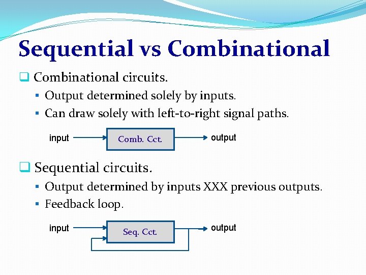
Sequential vs Combinational q Combinational circuits. § Output determined solely by inputs. § Can draw solely with left-to-right signal paths. input Comb. Cct. output q Sequential circuits. § Output determined by inputs XXX previous outputs. § Feedback loop. input Seq. Cct. output

Flip-flop & Register § Latches § Edge-triggered flip-flops § Master-slave flip-flops § Flip-flop operating characteristics § Flip-flop applications § One-shots § The 555 timer

Introduction q. Latches and FFs are the basic single-bit memory elements used to build sequential circuit with one or two inputs/outputs, designed using individual logic gates and feedback loops. q. Latches: q. The output of a latch depends on its current inputs and on its previous output and its change of state can happen at any time when its inputs change. q FFs: q. The output of a flip-flop also depends on current inputs and its previous output but the change of state occurs at specific times determined by a clock input.

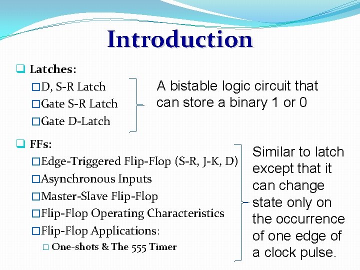
Introduction q Latches: �D, S-R Latch �Gate D-Latch A bistable logic circuit that can store a binary 1 or 0 q FFs: �Edge-Triggered Flip-Flop (S-R, J-K, D) �Asynchronous Inputs �Master-Slave Flip-Flop �Flip-Flop Operating Characteristics �Flip-Flop Applications: � One-shots & The 555 Timer Similar to latch except that it can change state only on the occurrence of one edge of a clock pulse.

Latches �Type of temporary storage device that has two stable (bi-stable) states �Similar to flip-flop – the outputs are connected back to opposite inputs �Main difference from flip-flop is the method used for changing their state �Includes: S-R latch, Gated/Enabled S-R latch and Gated D latch

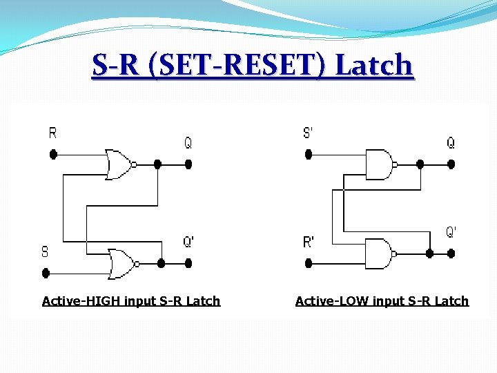
S-R (SET-RESET) Latch Active-HIGH input S-R Latch Active-LOW input S-R Latch

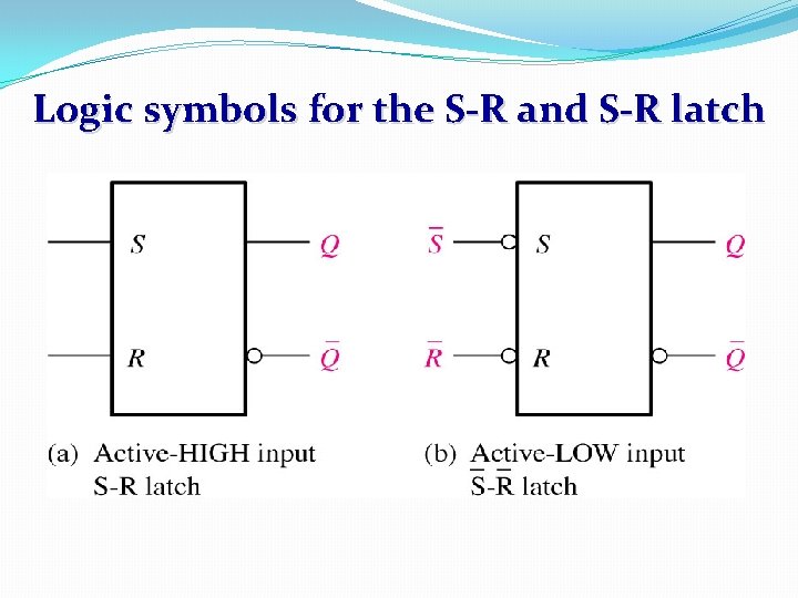
Logic symbols for the S-R and S-R latch

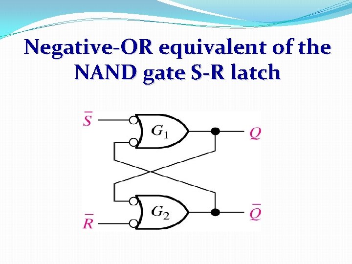
Negative-OR equivalent of the NAND gate S-R latch


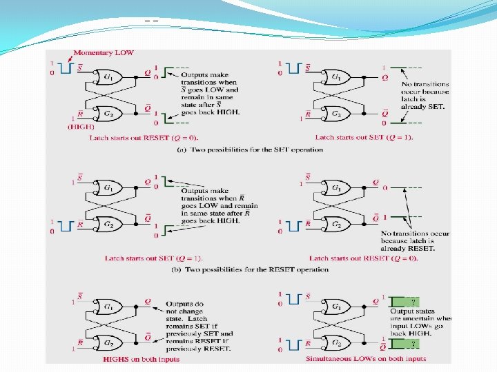
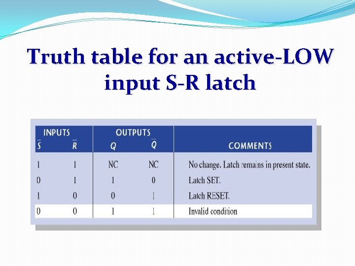
Truth table for an active-LOW input S-R latch

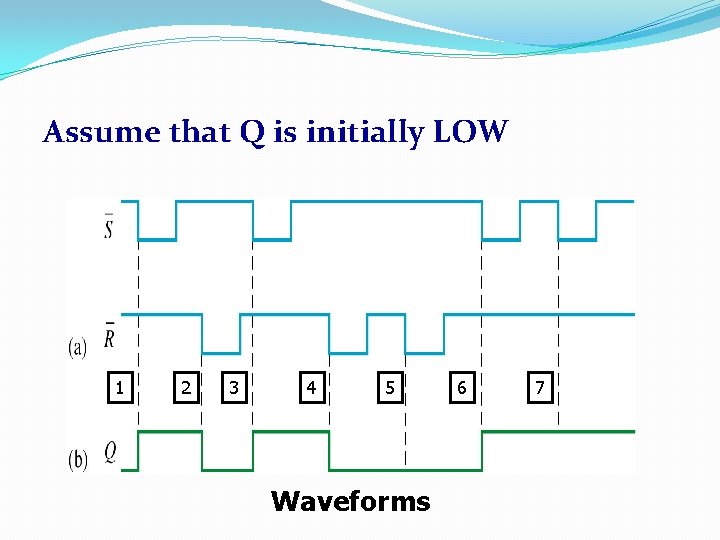
Assume that Q is initially LOW 1 2 3 4 5 Waveforms 6 7

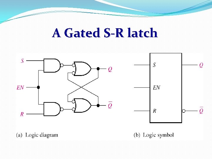
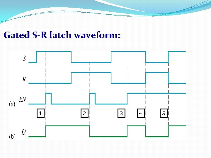
Gated S-R Latch q A gate input is added to the S-R latch to make the latch synchronous. q In order for the set and reset inputs to change the latch, the gate input must be active (high/Enable). q When the gate input is low, the latch remains in the hold condition.

A Gated S-R latch

Gated S-R latch waveform: 1 2 3 4 5

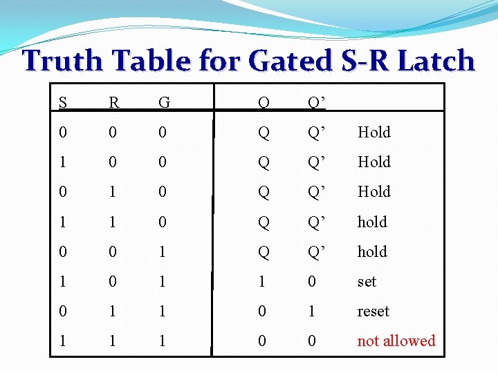
Truth Table for Gated S-R Latch S R G Q Q’ 0 0 0 Q Q’ Hold 1 0 0 Q Q’ Hold 0 1 0 Q Q’ Hold 1 1 0 Q Q’ hold 0 0 1 Q Q’ hold 1 0 1 1 0 set 0 1 1 0 1 reset 1 1 1 0 0 not allowed

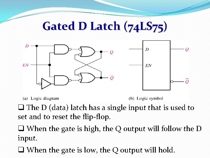
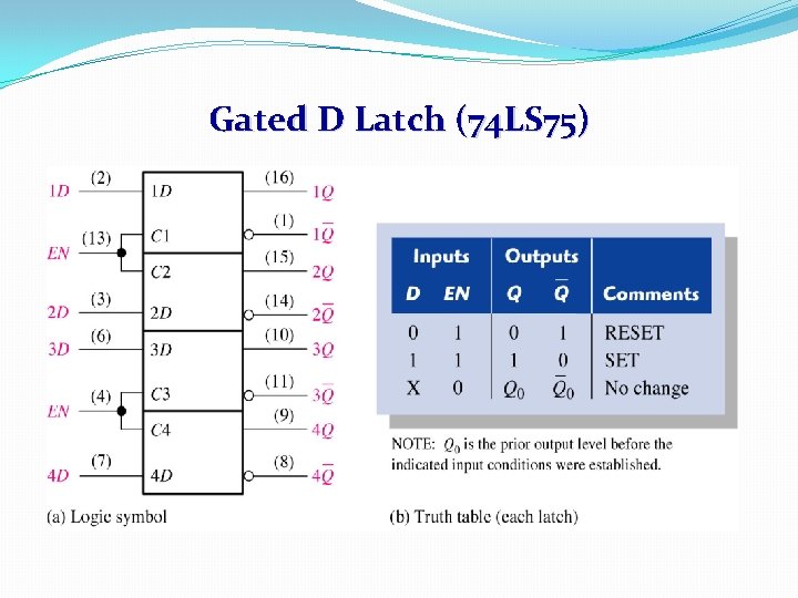
Gated D Latch (74 LS 75) q The D (data) latch has a single input that is used to set and to reset the flip-flop. q When the gate is high, the Q output will follow the D input. q When the gate is low, the Q output will hold.

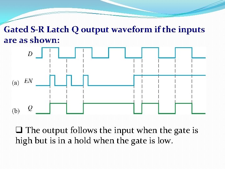
Gated S-R Latch Q output waveform if the inputs are as shown: q The output follows the input when the gate is high but is in a hold when the gate is low.

Gated D Latch (74 LS 75)

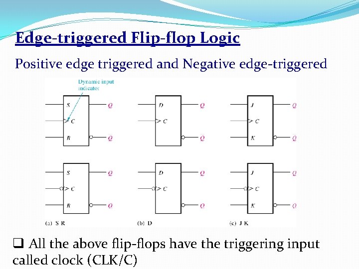
Edge-triggered Flip-flop Logic Positive edge triggered and Negative edge-triggered q All the above flip-flops have the triggering input called clock (CLK/C)

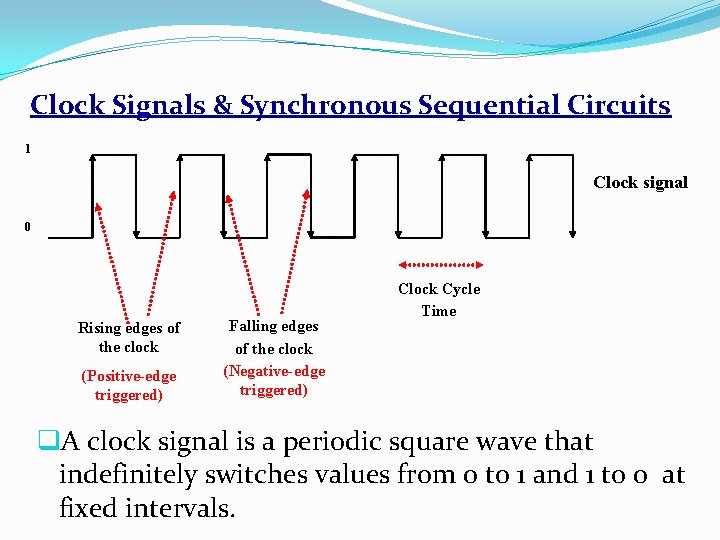
Clock Signals & Synchronous Sequential Circuits 1 Clock signal 0 Rising edges of the clock (Positive-edge triggered) Falling edges of the clock (Negative-edge triggered) Clock Cycle Time q. A clock signal is a periodic square wave that indefinitely switches values from 0 to 1 and 1 to 0 at fixed intervals.

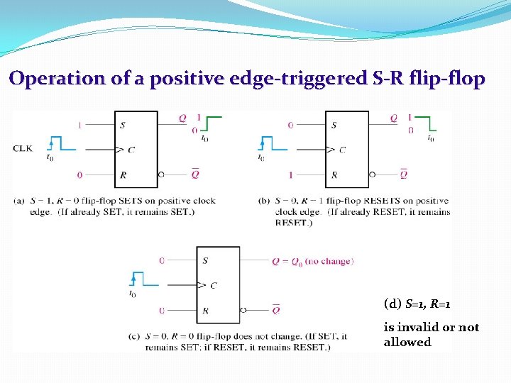
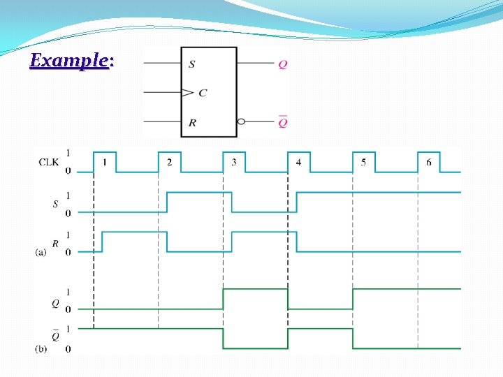
Operation of a positive edge-triggered S-R flip-flop (d) S=1, R=1 is invalid or not allowed

Example:

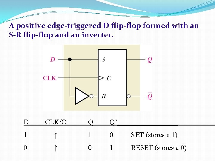
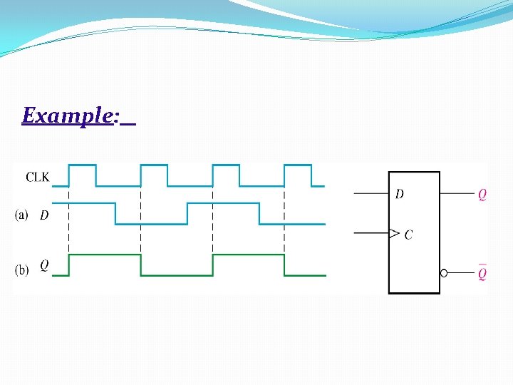
A positive edge-triggered D flip-flop formed with an S-R flip-flop and an inverter. D CLK/C Q Q’_________ 1 ↑ 1 0 SET (stores a 1) 0 ↑ 0 1 RESET (stores a 0)

Example:

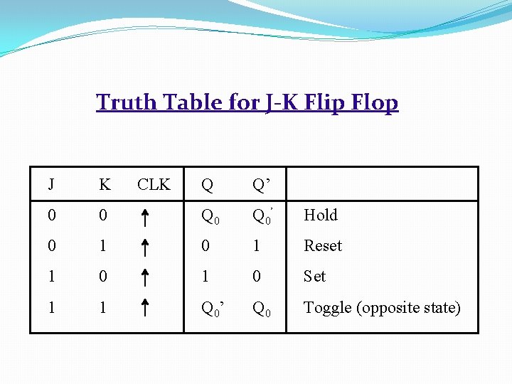
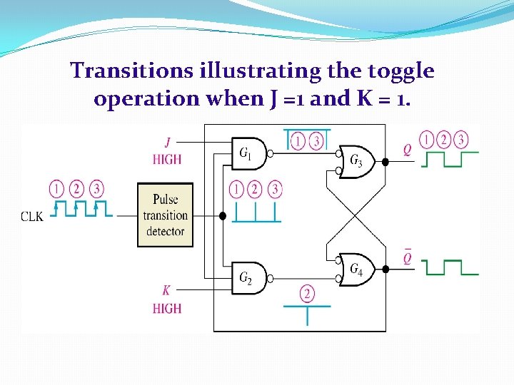
Truth Table for J-K Flip Flop J K 0 CLK Q Q’ 0 Q 0’ Hold 0 1 Reset 1 0 Set 1 1 Q 0’ Q 0 Toggle (opposite state)

Transitions illustrating the toggle operation when J =1 and K = 1.

Edge-triggered J-K flip-flop q The edge-triggered J-K will only accept the J and inputs during the active edge of the clock. q The small triangle on the clock input indicates that the device is edge-triggered. q A bubble on the clock input indicates that the device responds to the negative edge. no bubble would indicate a positive edge-triggered device.

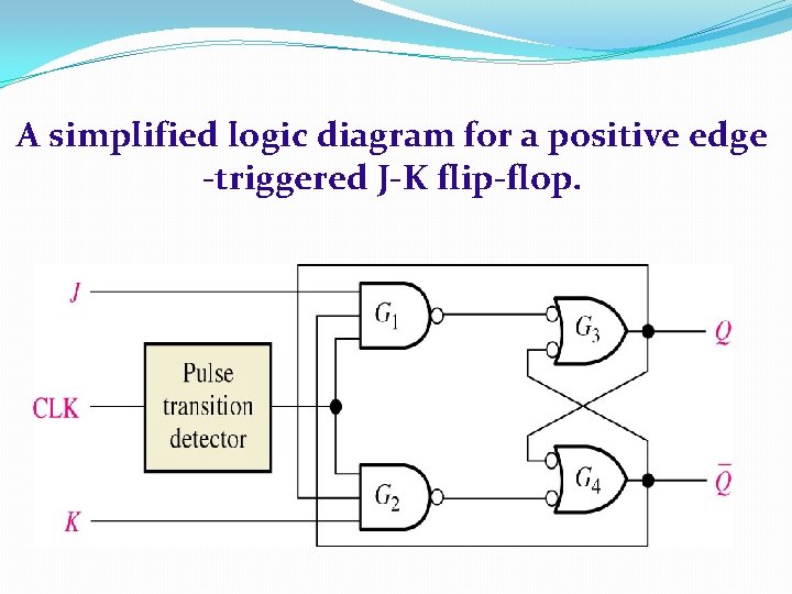
A simplified logic diagram for a positive edge -triggered J-K flip-flop.

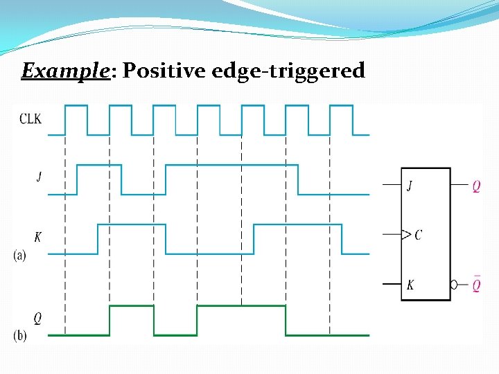
Example: Positive edge-triggered

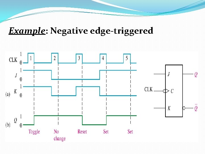
Example: Negative edge-triggered

Preset and Clear Inputs q For D , J-K FFs, the inputs are called synchronous input because the state of this inputs control the output only on the triggering edge of clock pulse. (with synch. clock) q Most IC FFs also have asynchronous inputs that change the output w/o a clock pulse. (work independently of clock) q Two Asynch. Inputs: preset (PRE) and clear (CLR) q Some cases called direct set (SD) and direct reset (RD) q When PRE is active, FF is SET q When CLR is active, FF is RESET regardless of the other inputs. q Usually, asynch. inputs are active-LOW inputs, indicated

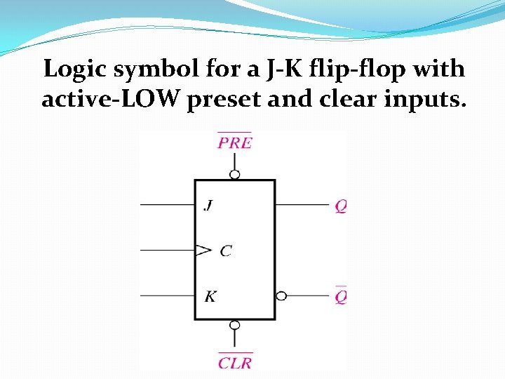
Logic symbol for a J-K flip-flop with active-LOW preset and clear inputs.

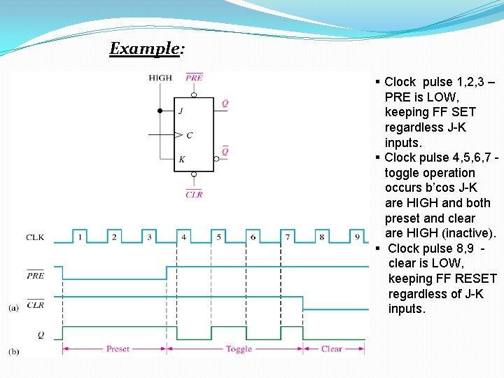
Example: § Clock pulse 1, 2, 3 – PRE is LOW, keeping FF SET regardless J-K inputs. § Clock pulse 4, 5, 6, 7 toggle operation occurs b’cos J-K are HIGH and both preset and clear are HIGH (inactive). § Clock pulse 8, 9 clear is LOW, keeping FF RESET regardless of J-K inputs.

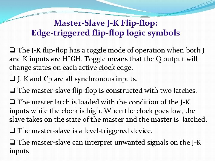
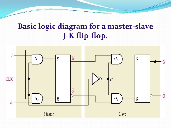
Master-Slave J-K Flip-flop: Edge-triggered flip-flop logic symbols q The J-K flip-flop has a toggle mode of operation when both J and K inputs are HIGH. Toggle means that the Q output will change states on each active clock edge. q J, K and Cp are all synchronous inputs. q The master-slave flip-flop is constructed with two latches. q The master latch is loaded with the condition of the J-K inputs while the clock is high. When the clock goes low, the slave takes on the state of the master and the master is latched. q The master-slave is a level-triggered device. q The master-slave can interpret unwanted signals on the J-K inputs.

Basic logic diagram for a master-slave J-K flip-flop.

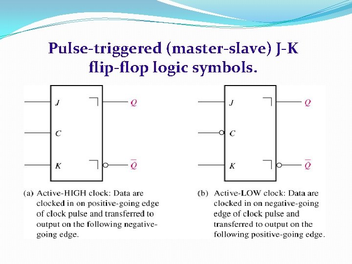
Pulse-triggered (master-slave) J-K flip-flop logic symbols.

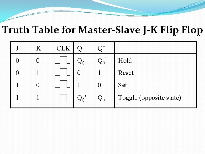
Truth Table for Master-Slave J-K Flip Flop J K 0 CLK Q Q’ 0 Q 0’ Hold 0 1 Reset 1 0 Set 1 1 Q 0’ Q 0 Toggle (opposite state)

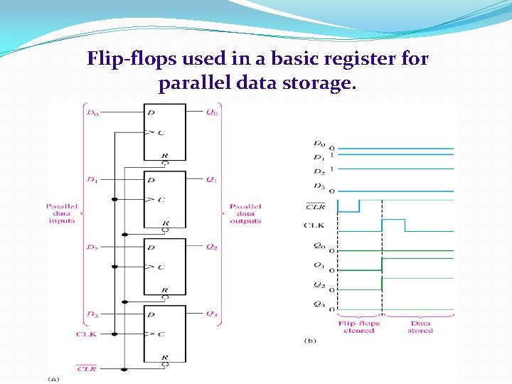
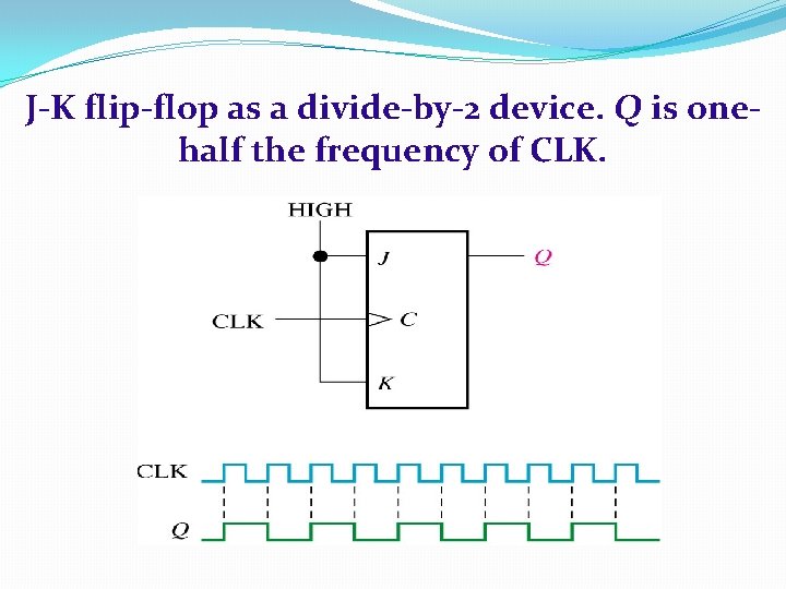
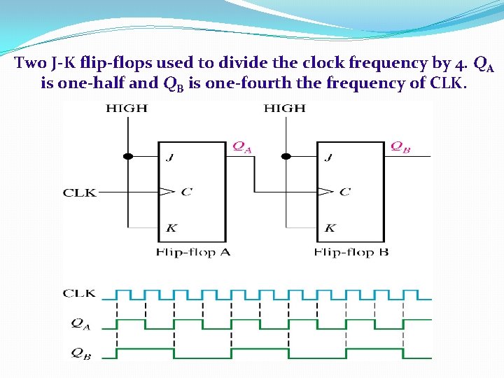
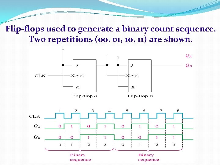
Flip-Flop Applications q Parallel Data Storage q Frequency Division q Counting

Flip-flops used in a basic register for parallel data storage.

J-K flip-flop as a divide-by-2 device. Q is onehalf the frequency of CLK.

Two J-K flip-flops used to divide the clock frequency by 4. QA is one-half and QB is one-fourth the frequency of CLK.

Flip-flops used to generate a binary count sequence. Two repetitions (00, 01, 10, 11) are shown.

Flip-Flop Operating Characteristics q. Propagation Delay Times q. Set-up Time q. Hold Time q. Maximum Clock Frequency q. Pulse Width q. Power Dissipation

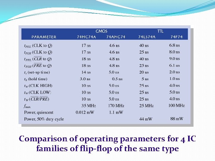
Comparison of operating parameters for 4 IC families of flip-flop of the same type

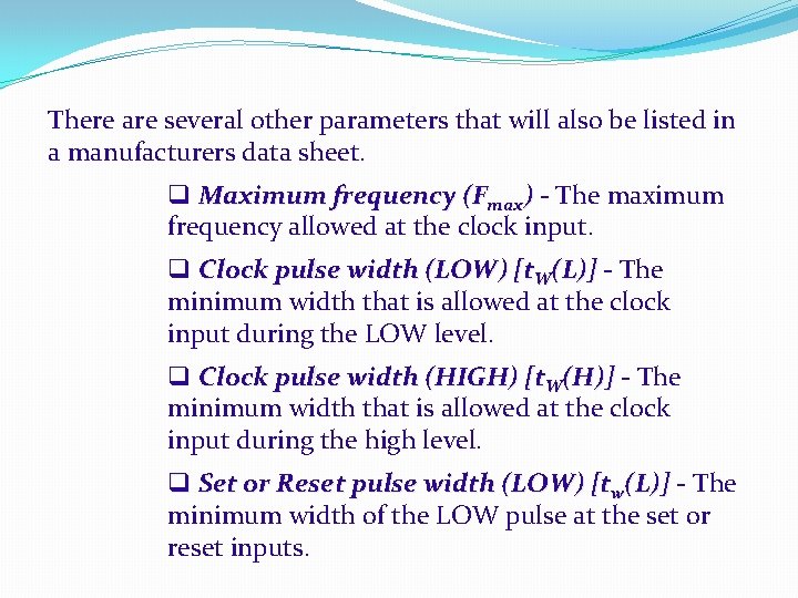
There are several other parameters that will also be listed in a manufacturers data sheet. q Maximum frequency (Fmax) - The maximum frequency allowed at the clock input. q Clock pulse width (LOW) [t. W(L)] - The minimum width that is allowed at the clock input during the LOW level. q Clock pulse width (HIGH) [t. W(H)] - The minimum width that is allowed at the clock input during the high level. q Set or Reset pulse width (LOW) [tw(L)] - The minimum width of the LOW pulse at the set or reset inputs.

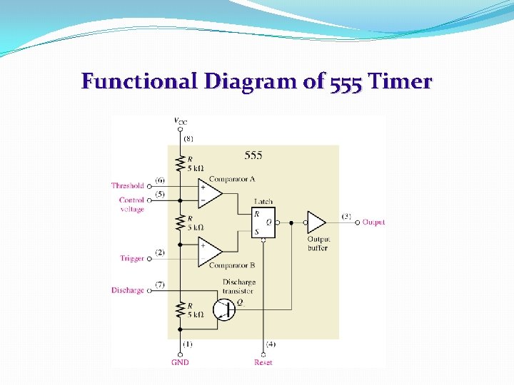
Basic operation of a 555 Timer q. Threshold q. Control Voltage q. Trigger q. Discharge q. Reset q. Output

Functional Diagram of 555 Timer

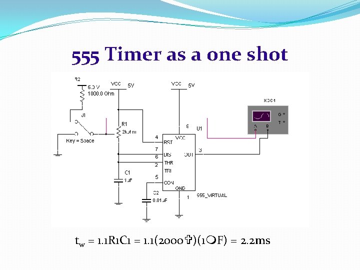
555 Timer as a one shot tw = 1. 1 R 1 C 1 = 1. 1(2000 )(1 F) = 2. 2 ms

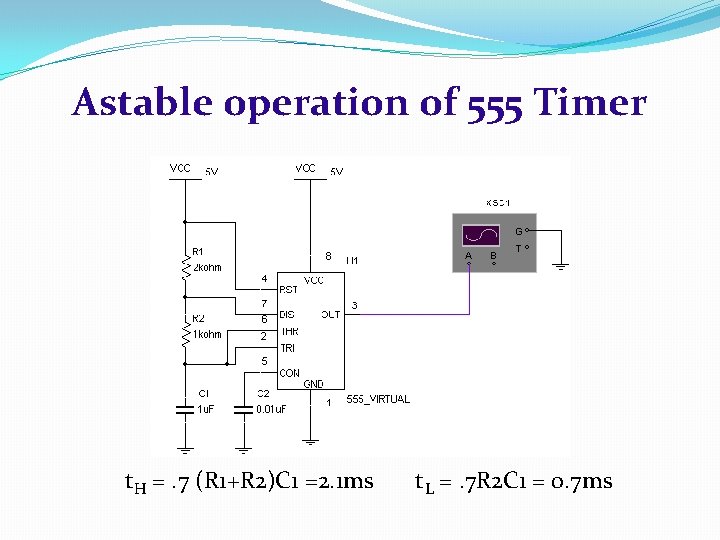
Astable operation of 555 Timer t. H =. 7 (R 1+R 2)C 1 =2. 1 ms t. L =. 7 R 2 C 1 = 0. 7 ms