EKT 104 Analog Electronic Circuits 1 BJT AC

EKT 104 Analog Electronic Circuits 1 BJT AC Analysis Chapter 1

BJT Transistor Modeling A model is an equivalent circuit that represents the AC characteristics of the transistor. A model uses circuit elements that approximate the behavior of the transistor. There are two models commonly used in small signal AC analysis of a transistor: re model Hybrid equivalent model

AC Equivalent Model AC equivalent model is obtained by: 1. Setting all dc sources to zero and replacing them by a short-circuit equivalent. 2. Replacing all capacitors by short-circuit equivalent. 3. Removing all elements bypassed by the shortcircuit equivalents introduced by steps 1 and 2. 4. Redrawing the network in a more convenient and logical form.
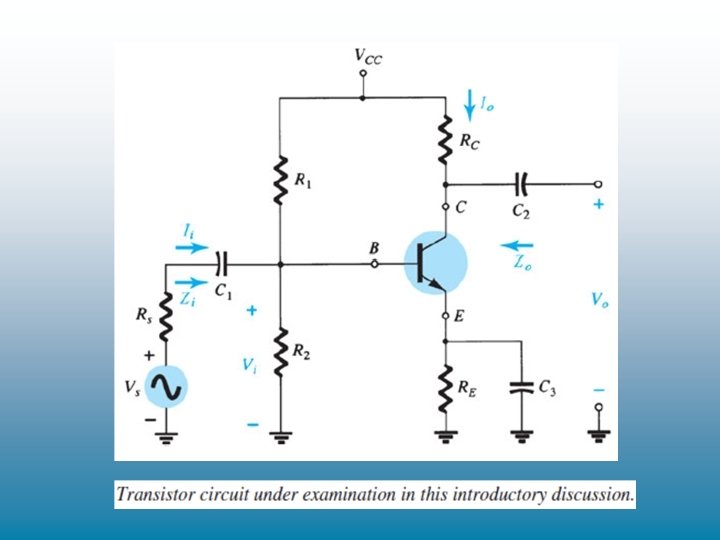

Applying Steps 1, 2 and 3: Resulting small-signal AC equivalent circuit, after removal of dc supply and insertion of short-circuit equivalent for capacitors.

Applying Step 4: Small-signal AC equivalent circuit.

Two-Port System: Two-Port System Small-signal AC equivalent circuit.

The re Transistor Model • BJTs are basically current-controlled devices; therefore the re model uses a diode and a current source to duplicate the behavior of the transistor. • One disadvantage to this model is its sensitivity to the DC level. This model is designed for specific circuit conditions. • Model: i. ii. iii. Common-base configuration Common-emitter configuration Common-collector configuration (use model defined by CE configuration).

re Model for Common-Base Configuration
 Diode can be replaced by its eqv.")
re Model for Common-Base Configuration (cntd. ) Diode can be replaced by its eqv. ac resistor, re. Common-Base re equivalent circuit. Voltage gain, Av : Current gain, Ai :

Example:

Solution:

re Model for Common-Emitter Configuration Common-Emitter re equivalent circuit.
 •")
re Model for Common-Emitter Configuration (cntd. ) •
 Common-Emitter re equivalent circuit. Voltage gain, Av")
re Model for Common-Emitter Configuration (cntd. ) Common-Emitter re equivalent circuit. Voltage gain, Av : Current gain, Ai :
. Input impedance,")
re Model for Common-Collector Configuration re equivalent circuit (based on CE configuration). Input impedance, Zi : Voltage gain, Av : Output impedance, Zo : Current gain, Ai :

Common-Emitter Fixed-Bias Configuration The input is applied to the base The output is taken from the collector Low input impedance High output impedance High voltage and current gain Phase shift between input and output is 180

Common-Emitter Fixed-Bias Configuration AC equivalent re model

Common-Emitter Fixed-Bias Calculations Input impedance: Output impedance: Voltage gain: Current gain: Current gain from voltage gain:

Example:

Solution:

Common-Emitter Voltage-Divider Bias re model requires you to determine , re, and ro.

Common-Emitter Voltage-Divider Bias Calculations Input impedance Voltage gain Output impedance Current gain from Av Current gain

Example:

Solution:

Common-Emitter-Bias Configuration

Impedance Calculations Input impedance: Output impedance:

Gain Calculations Voltage gain: Current gain from Av:

Emitter-Follower Configuration • This is also known as the common-collector configuration. • The input is applied to the base and the output is taken from the emitter. • There is no phase shift between input and output (thus, named as emitter -follower).

Impedance Calculations Input impedance: Output impedance:

Gain Calculations Voltage gain: Current gain from voltage gain:

Common-Base Configuration The input is applied to the emitter The output is taken from the collector Low input impedance. High output impedance Current gain less than unity Very high voltage gain No phase shift between input and output

Calculations Input impedance: Output impedance: Voltage gain: Current gain:

Effect of RL and RS
 •")
Effect of RL and RS (cntd) •

Effect of RL and RS in Fixed-Bias Configuration Original circuit to re equivalent circuit.

Effect of RL and RS in Fixed-Bias Configuration Input impedance, Zi : Output impedance, Zo :

Effect of RL and RS in Fixed-Bias Configuration Loaded gain, Av. L : Overall gain, Avs :

Effect of RL and RS in Fixed-Bias Configuration Current gain, Ai. L : Overall current gain, Ais :

Effect of RL and RS in Voltage-Divider Configuration Original circuit to re equivalent circuit.

Effect of RL and RS in Voltage-Divider Configuration Input impedance, Zi : Output impedance, Zo : Loaded gain, Av. L : Overall gain, Avs :
- Slides: 42