Efficient Circuit Architecture and FPGA Implementation for LTE
- Slides: 16

Efficient Circuit Architecture and FPGA Implementation for LTE Single Carrier FDMA DFT J. Greg Nash www. centar. net jgregnash@centar. net SOCC 2016

Outline • Motivation? • Wireless protocol: LTE Single Carrier Frequency Division Multiplex • Review of FFT architectures • New FFT architecture • Circuit FPGA performance comparisons – Altera – Xilinx • Conclusions

Motivation • Future connectivity – “Internet Of Things”, e. g. , every device with on/off switch gets connected to the internet – Gartner says that by 2020 there will be over 26 billion connected devices – Wireless OFDM protocols (LTE, … etc. ) are responsible for mobile connections • Expanding FPGA markets – Altera: 44% sales in Telecom and Wireless – Growth in mobile applications for FPGAs (Lattice Semiconductor)

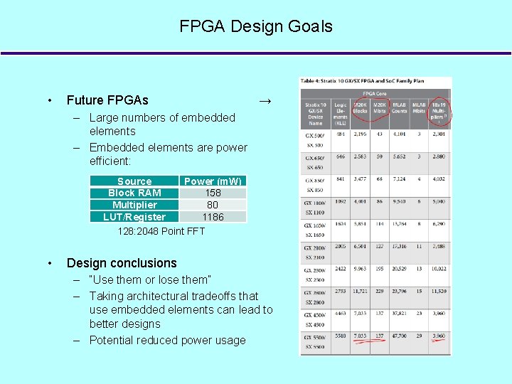
FPGA Design Goals • Future FPGAs → – Large numbers of embedded elements – Embedded elements are power efficient: Source Power (m. W) Block RAM 158 Multiplier 80 LUT/Register 1186 128: 2048 Point FFT • Design conclusions – “Use them or lose them” – Taking architectural tradeoffs that use embedded elements can lead to better designs – Potential reduced power usage

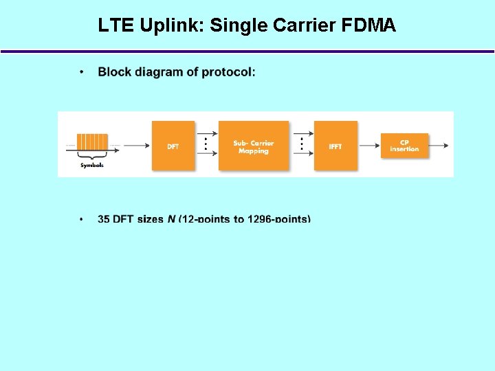
LTE Uplink: Single Carrier FDMA •

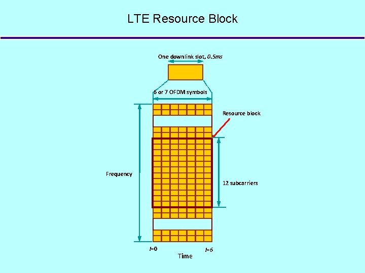
LTE Resource Block One downlink slot, 0. 5 ms 6 or 7 OFDM symbols Resource block : Frequency 12 subcarriers : l=0 Time l=6

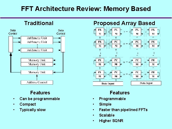
FFT Architecture Review: Memory Based Traditional Proposed Array Based Features • • • Can be programmable Compact Typically slow Features • • • Programmable Simple Faster than pipelined FFTs Scalable Higher SQNR

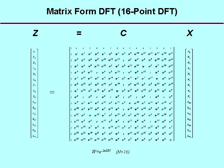
Matrix Form DFT (16 -Point DFT) Z = C W=e-2πI/N (N=16) X

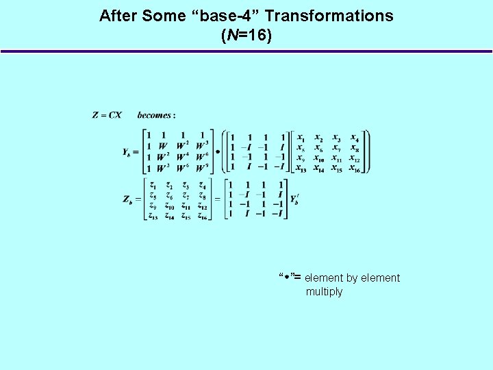
After Some “base-4” Transformations (N=16) “ ”= element by element multiply

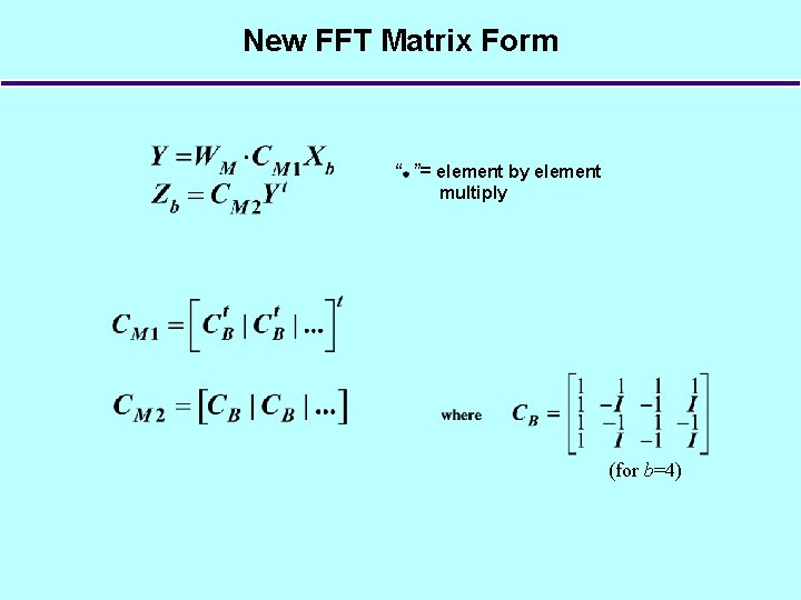
New FFT Matrix Form “ ”= element by element multiply (for b=4)

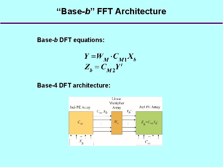
“Base-b” FFT Architecture Base-b DFT equations: Base-4 DFT architecture:

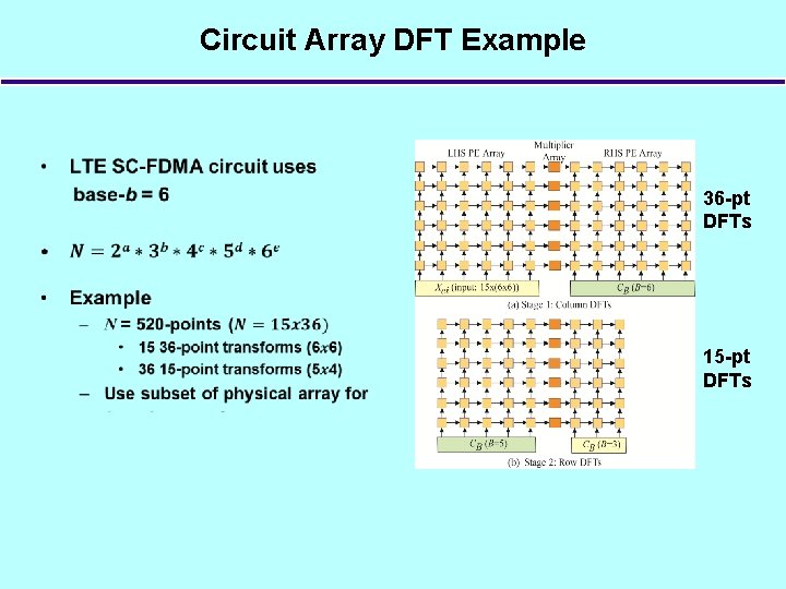
Circuit Array DFT Example • 36 -pt DFTs 15 -pt DFTs

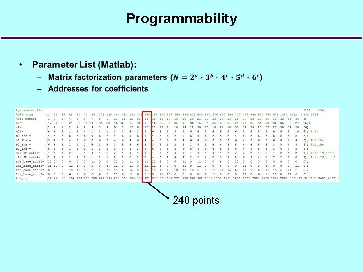
Programmability • 240 points

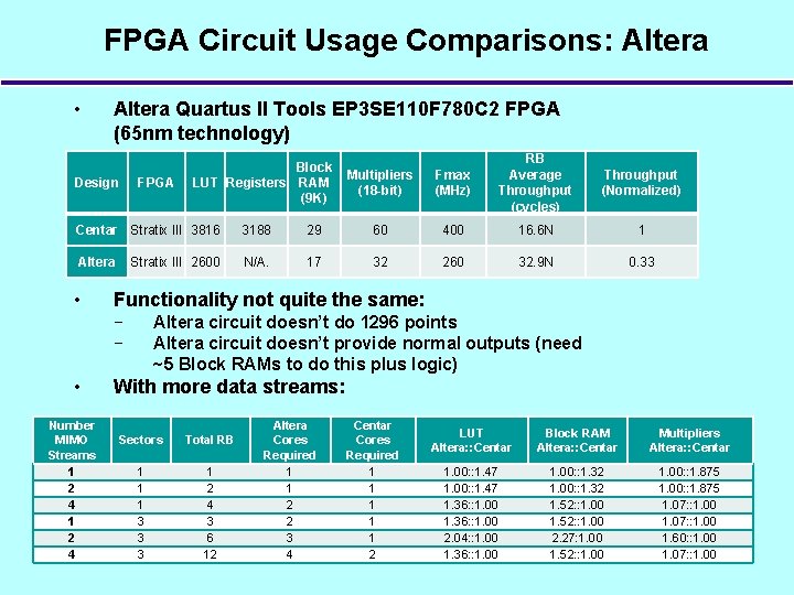
FPGA Circuit Usage Comparisons: Altera • Altera Quartus II Tools EP 3 SE 110 F 780 C 2 FPGA (65 nm technology) Design FPGA Block LUT Registers RAM (9 K) Multipliers (18 -bit) Fmax (MHz) RB Average Throughput (cycles) Throughput (Normalized) Centar Stratix III 3816 3188 29 60 400 16. 6 N 1 Altera N/A. 17 32 260 32. 9 N 0. 33 • Stratix III 2600 Functionality not quite the same: − − • Number MIMO Streams 1 2 4 Altera circuit doesn’t do 1296 points Altera circuit doesn’t provide normal outputs (need ~5 Block RAMs to do this plus logic) With more data streams: Sectors Total RB 1 1 1 3 3 3 1 2 4 3 6 12 Altera Cores Required 1 1 2 2 3 4 Centar Cores Required 1 1 1 2 LUT Altera: : Centar Block RAM Altera: : Centar Multipliers Altera: : Centar 1. 00: : 1. 47 1. 36: : 1. 00 2. 04: : 1. 00 1. 36: : 1. 00: : 1. 32 1. 52: : 1. 00 2. 27: 1. 00 1. 52: : 1. 00: : 1. 875 1. 07: : 1. 00 1. 60: : 1. 00 1. 07: : 1. 00

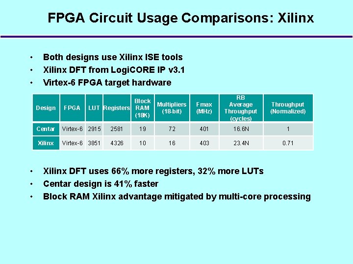
FPGA Circuit Usage Comparisons: Xilinx • • • Both designs use Xilinx ISE tools Xilinx DFT from Logi. CORE IP v 3. 1 Virtex-6 FPGA target hardware Design • • • FPGA Block LUT Registers RAM (18 K) Multipliers (18 -bit) Fmax (MHz) RB Average Throughput (cycles) Throughput (Normalized) Centar Virtex-6 2915 2581 19 72 401 16. 6 N 1 Xilinx Virtex-6 3851 4326 10 16 403 23. 4 N 0. 71 Xilinx DFT uses 66% more registers, 32% more LUTs Centar design is 41% faster Block RAM Xilinx advantage mitigated by multi-core processing

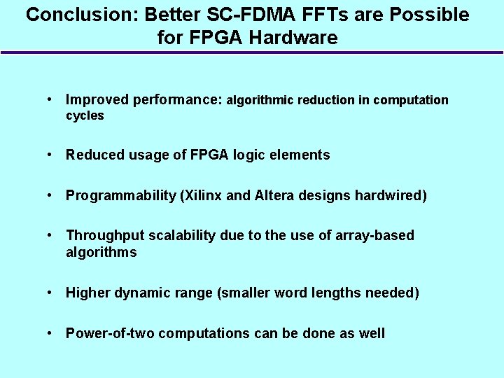
Conclusion: Better SC-FDMA FFTs are Possible for FPGA Hardware • Improved performance: algorithmic reduction in computation cycles • Reduced usage of FPGA logic elements • Programmability (Xilinx and Altera designs hardwired) • Throughput scalability due to the use of array-based algorithms • Higher dynamic range (smaller word lengths needed) • Power-of-two computations can be done as well