Effectiveness Measures for VLSI Testing Defective Parts per
- Slides: 24

Effectiveness Measures for VLSI Testing: Defective Parts per Million, Defect Coverage and Fault Coverage Vishwani D. Agrawal James J. Danaher Professor Department of Electrical and Computer Engineering Auburn University, Auburn, AL 36849 http: //www. eng. auburn. edu/~vagrawal@eng. auburn. edu Oct. 24, 2007 Agrawal: VLSI Testing Effectiveness 1

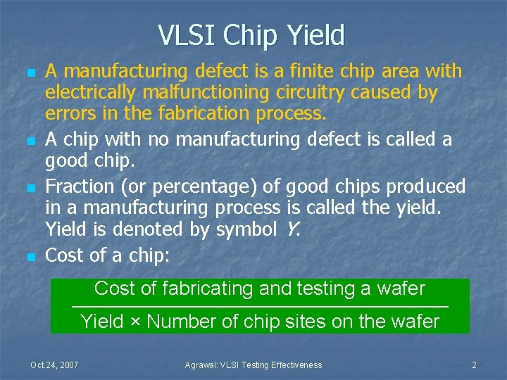
VLSI Chip Yield n n A manufacturing defect is a finite chip area with electrically malfunctioning circuitry caused by errors in the fabrication process. A chip with no manufacturing defect is called a good chip. Fraction (or percentage) of good chips produced in a manufacturing process is called the yield. Yield is denoted by symbol Y. Cost of a chip: Cost of fabricating and testing a wafer Yield × Number of chip sites on the wafer Oct. 24, 2007 Agrawal: VLSI Testing Effectiveness 2

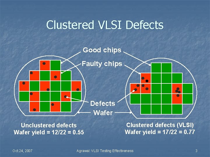
Clustered VLSI Defects Good chips Faulty chips Defects Wafer Unclustered defects Wafer yield = 12/22 = 0. 55 Oct. 24, 2007 Clustered defects (VLSI) Wafer yield = 17/22 = 0. 77 Agrawal: VLSI Testing Effectiveness 3

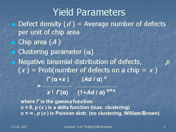
Yield Parameters n n Defect density (d ) = Average number of defects per unit of chip area Chip area (A ) Clustering parameter (a) Negative binomial distribution of defects, p (x ) = Prob(number of defects on a chip = x ) Γ (α +x ) (Ad / α) x = . x ! Γ (α) (1+Ad / α) α+x where Γ is the gamma function α = 0, p (x ) is a delta function (max. clustering) α = , p (x ) is Poisson distr. (no clustering, William/Brown) Oct. 24, 2007 Agrawal: VLSI Testing Effectiveness 4

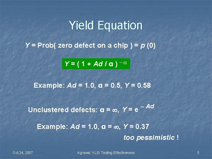
Yield Equation Y = Prob( zero defect on a chip ) = p (0) Y = ( 1 + Ad / α ) – α Example: Ad = 1. 0, α = 0. 5, Y = 0. 58 Unclustered defects: α = , Y = e – Ad Example: Ad = 1. 0, α = , Y = 0. 37 too pessimistic ! Oct. 24, 2007 Agrawal: VLSI Testing Effectiveness 5

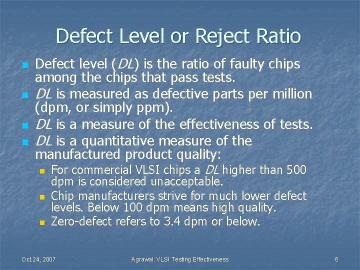
Defect Level or Reject Ratio n n Defect level (DL) is the ratio of faulty chips among the chips that pass tests. DL is measured as defective parts per million (dpm, or simply ppm). DL is a measure of the effectiveness of tests. DL is a quantitative measure of the manufactured product quality: n n n For commercial VLSI chips a DL higher than 500 dpm is considered unacceptable. Chip manufacturers strive for much lower defect levels. Below 100 dpm means high quality. Zero-defect refers to 3. 4 dpm or below. Oct. 24, 2007 Agrawal: VLSI Testing Effectiveness 6

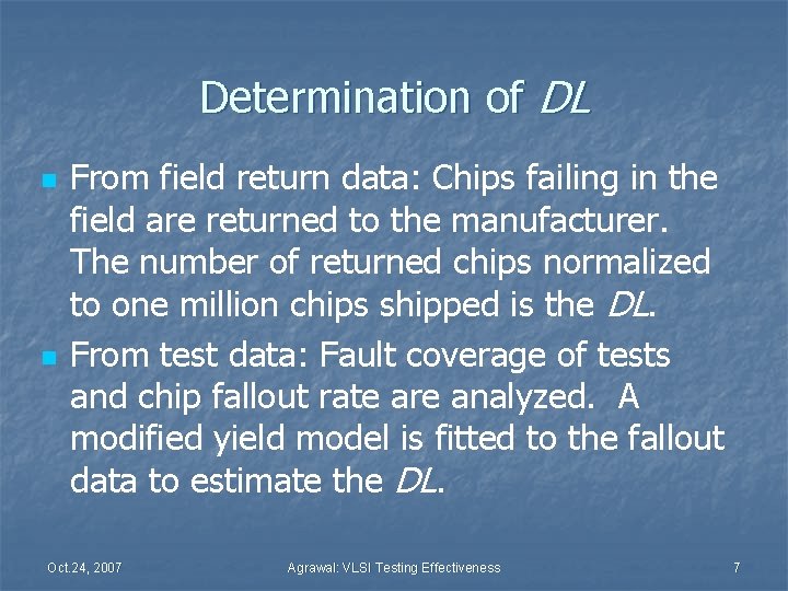
Determination of DL n n From field return data: Chips failing in the field are returned to the manufacturer. The number of returned chips normalized to one million chips shipped is the DL. From test data: Fault coverage of tests and chip fallout rate are analyzed. A modified yield model is fitted to the fallout data to estimate the DL. Oct. 24, 2007 Agrawal: VLSI Testing Effectiveness 7

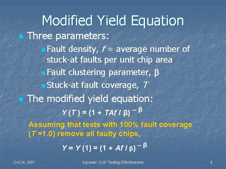
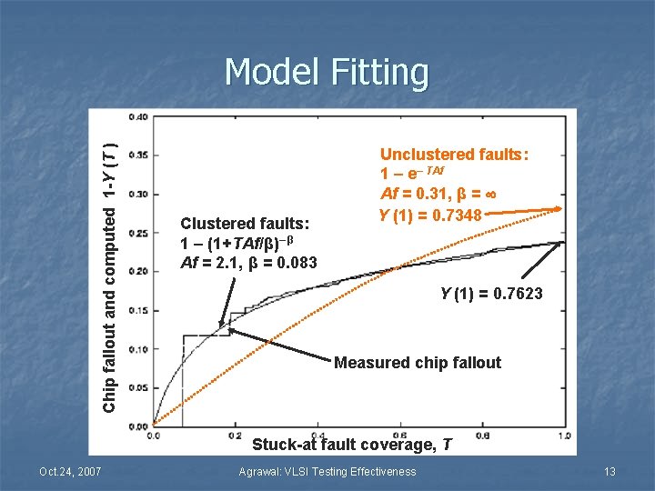
Modified Yield Equation n Three parameters: density, f = average number of stuck-at faults per unit chip area n Fault clustering parameter, b n Stuck-at fault coverage, T n Fault n The modified yield equation: Y (T ) = (1 + TAf / β) – β Assuming that tests with 100% fault coverage (T =1. 0) remove all faulty chips, Y = Y (1) = (1 + Af / β) – β Oct. 24, 2007 Agrawal: VLSI Testing Effectiveness 8

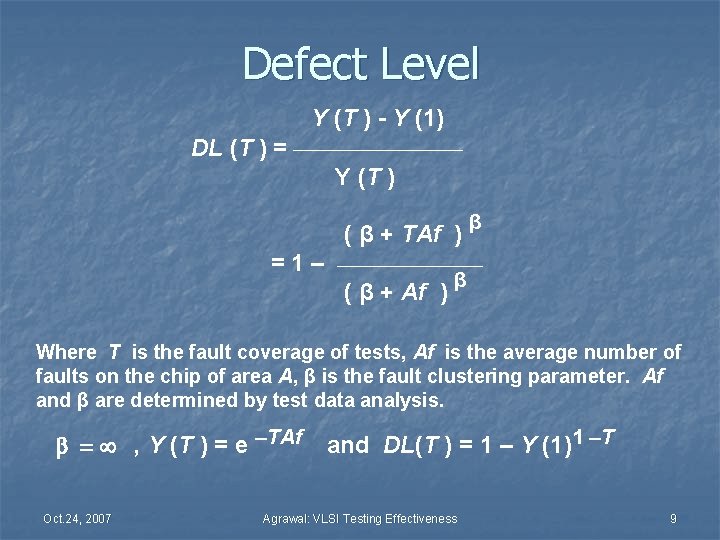
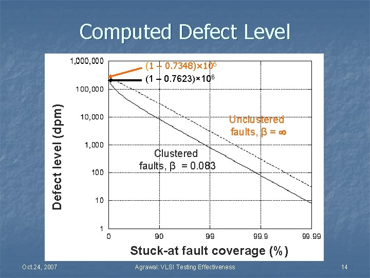
Defect Level Y (T ) - Y (1) DL (T ) = Y (T ) ( β + TAf ) =1– β ( β + Af ) β Where T is the fault coverage of tests, Af is the average number of faults on the chip of area A, β is the fault clustering parameter. Af and β are determined by test data analysis. b = , Y (T ) = e –TAf Oct. 24, 2007 and DL(T ) = 1 – Y (1)1 –T Agrawal: VLSI Testing Effectiveness 9

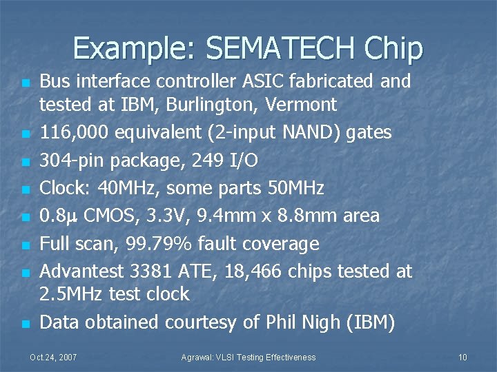
Example: SEMATECH Chip n n n n Bus interface controller ASIC fabricated and tested at IBM, Burlington, Vermont 116, 000 equivalent (2 -input NAND) gates 304 -pin package, 249 I/O Clock: 40 MHz, some parts 50 MHz 0. 8 m CMOS, 3. 3 V, 9. 4 mm x 8. 8 mm area Full scan, 99. 79% fault coverage Advantest 3381 ATE, 18, 466 chips tested at 2. 5 MHz test clock Data obtained courtesy of Phil Nigh (IBM) Oct. 24, 2007 Agrawal: VLSI Testing Effectiveness 10

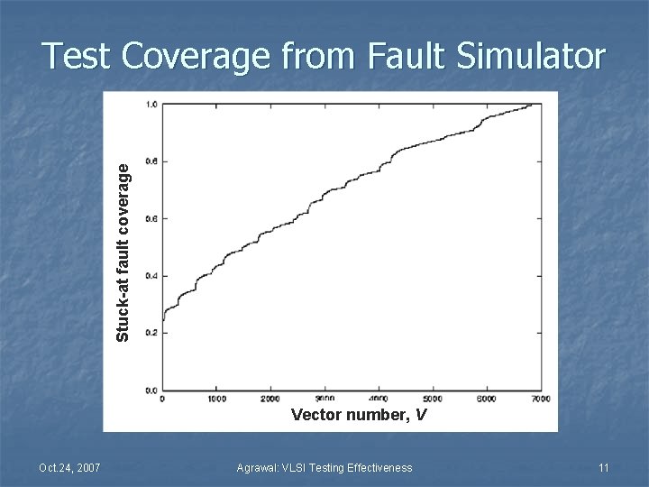
Stuck-at fault coverage Test Coverage from Fault Simulator Vector number, V Oct. 24, 2007 Agrawal: VLSI Testing Effectiveness 11

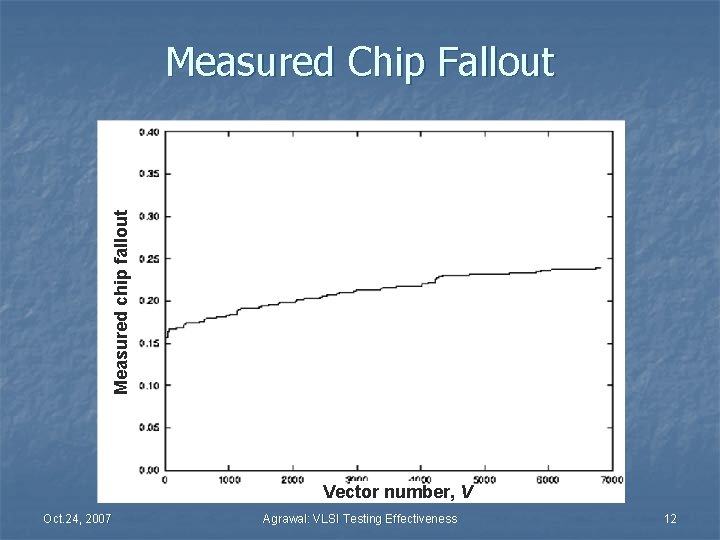
Measured chip fallout Measured Chip Fallout Vector number, V Oct. 24, 2007 Agrawal: VLSI Testing Effectiveness 12

Chip fallout and computed 1 -Y (T ) Model Fitting Clustered faults: 1 – (1+TAf/β)– β Af = 2. 1, β = 0. 083 Unclustered faults: 1 – e– TAf Af = 0. 31, β = Y (1) = 0. 7348 Y (1) = 0. 7623 Measured chip fallout Stuck-at fault coverage, T Oct. 24, 2007 Agrawal: VLSI Testing Effectiveness 13

Computed Defect Level Defect level (dpm) (1 – 0. 7348)× 106 (1 – 0. 7623)× 106 Unclustered faults, β = Clustered faults, β = 0. 083 Stuck-at fault coverage (%) Oct. 24, 2007 Agrawal: VLSI Testing Effectiveness 14

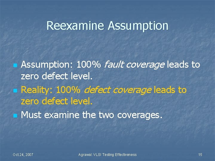
Reexamine Assumption n Assumption: 100% fault coverage leads to zero defect level. Reality: 100% defect coverage leads to zero defect level. Must examine the two coverages. Oct. 24, 2007 Agrawal: VLSI Testing Effectiveness 15

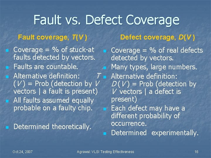
Fault vs. Defect Coverage Fault coverage, T(V ) n n n Coverage = % of stuck-at faults detected by vectors. Faults are countable. Alternative definition: T (V ) = Prob (detection by V vectors | a fault is present) All faults assumed equally probable on a faulty chip. Defect coverage, D(V ) n n Determined theoretically. n Oct. 24, 2007 Coverage = % of real defects detected by vectors. Many types, large numbers. Alternative definition: D (V ) = Prob (detection by V vectors | a defect is present) Each defect may have a different probability of occurrence. Determined experimentally. Agrawal: VLSI Testing Effectiveness 16

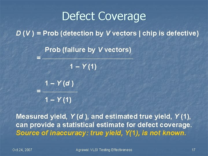
Defect Coverage D (V ) = Prob (detection by V vectors | chip is defective) Prob (failure by V vectors) = 1 – Y (1) 1 – Y (d ) = 1 – Y (1) Measured yield, Y (d ), and estimated true yield, Y (1), can provide a statistical estimate for defect coverage. Source of inaccuracy: true yield, Y(1), is not known. Oct. 24, 2007 Agrawal: VLSI Testing Effectiveness 17

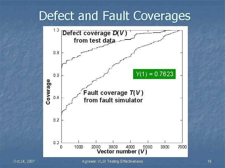
Defect and Fault Coverages Defect coverage D(V ) from test data Coverage Y(1) = 0. 7623 Fault coverage T(V ) from fault simulator Vector number (V ) Oct. 24, 2007 Agrawal: VLSI Testing Effectiveness 18

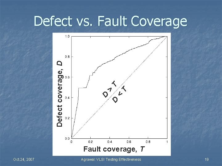
T T D < > D Defect coverage, D Defect vs. Fault Coverage Fault coverage, T Oct. 24, 2007 Agrawal: VLSI Testing Effectiveness 19

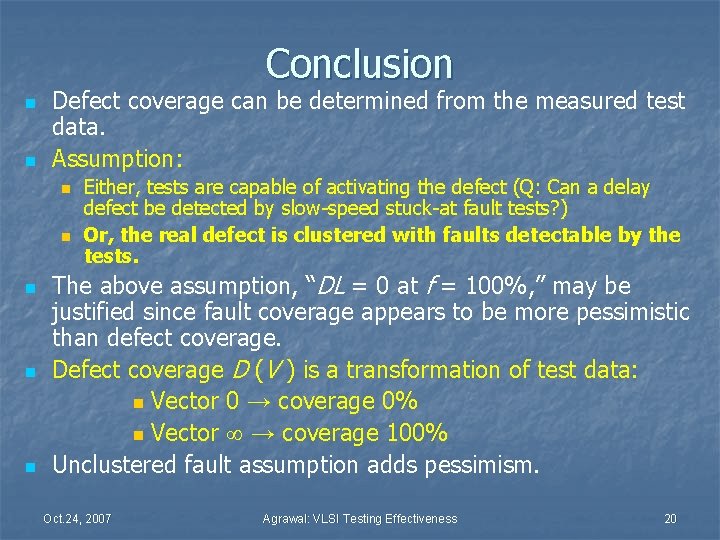
Conclusion n n Defect coverage can be determined from the measured test data. Assumption: n n n Either, tests are capable of activating the defect (Q: Can a delay defect be detected by slow-speed stuck-at fault tests? ) Or, the real defect is clustered with faults detectable by the tests. The above assumption, “DL = 0 at f = 100%, ” may be justified since fault coverage appears to be more pessimistic than defect coverage. Defect coverage D (V ) is a transformation of test data: n Vector 0 → coverage 0% n Vector → coverage 100% Unclustered fault assumption adds pessimism. Oct. 24, 2007 Agrawal: VLSI Testing Effectiveness 20

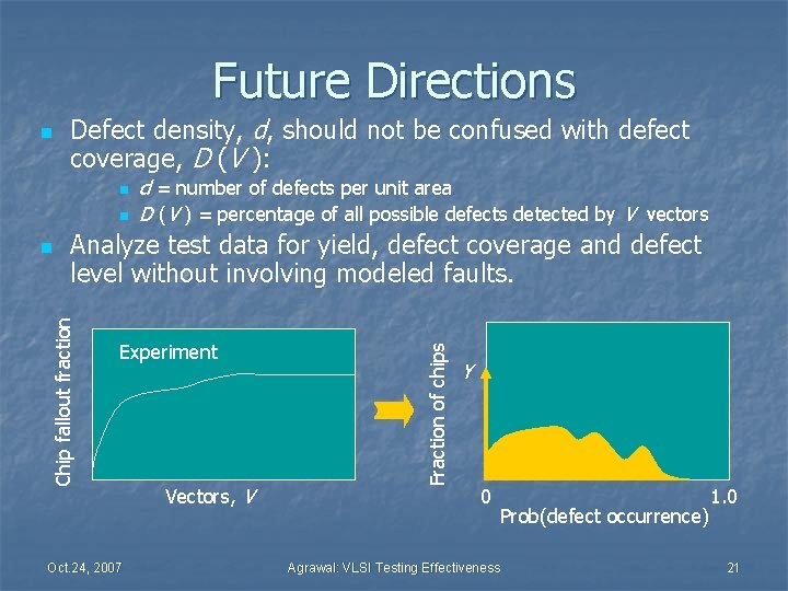
Future Directions Defect density, d, should not be confused with defect coverage, D (V ): n n Analyze test data for yield, defect coverage and defect level without involving modeled faults. Chip fallout fraction n d = number of defects per unit area D (V ) = percentage of all possible defects detected by V vectors Experiment Oct. 24, 2007 Vectors, V Fraction of chips n Y 0 Agrawal: VLSI Testing Effectiveness Prob(defect occurrence) 1. 0 21

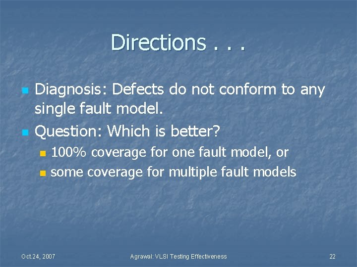
Directions. . . n n Diagnosis: Defects do not conform to any single fault model. Question: Which is better? n n 100% coverage for one fault model, or some coverage for multiple fault models Oct. 24, 2007 Agrawal: VLSI Testing Effectiveness 22

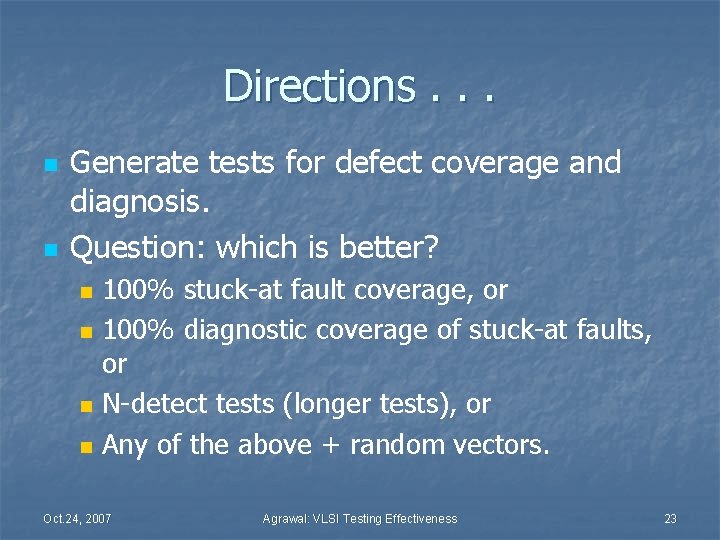
Directions. . . n n Generate tests for defect coverage and diagnosis. Question: which is better? n n 100% stuck-at fault coverage, or 100% diagnostic coverage of stuck-at faults, or N-detect tests (longer tests), or Any of the above + random vectors. Oct. 24, 2007 Agrawal: VLSI Testing Effectiveness 23

References n n The clustered fault model used for Sematech data is described in the book: M. L. Bushnell and V. D. Agrawal, Essentials of Electronic Testing for Digital, Memory and Mixed-Signal VLSI Circuits, Springer, 2000, Chapter 3. The unclustered defect model is from the paper: T. W. Williams and N. C. Brown, “Defect Level as a Function of Fault Coverage, ” IEEE Trans. Computers, vol. C-30, no. 12, pp. 987 -988, Dec. 1981. The discussion on defect coverage is from a presentation: J. T. de Sousa and V. D. Agrawal, “An Experimental Study of Tester Yield and Defect Coverage, ” IEEE International Test Synthesis Workshop, Santa Barbara, California, March 2001. A direct analysis of defect level without involving the stuck-at fault coverage is given in the paper: S. C. Seth and V. D. Agrawal, “On the Probability of Fault Occurrence, ” Defect and Fault Tolerance in VLSI Systems, I. Koren, editor, Plenum Publishing Corp. , 1989, pp. 47 -52. Oct. 24, 2007 Agrawal: VLSI Testing Effectiveness 24