Effect of proton fluence on radiation defect structure
![Material Orientation Type ρ(300 K) [Ωcm] <100> n 2200± 200 [P] [x 1012 cm-3] Material Orientation Type ρ(300 K) [Ωcm] <100> n 2200± 200 [P] [x 1012 cm-3]](https://slidetodoc.com/presentation_image_h2/b7b7ff83ad16bfe5cb29a425941350cb/image-3.jpg)
![FTIR, V 2 – concentration vs proton fluence Concentration [cm-3] 1, 0 E+16 V FTIR, V 2 – concentration vs proton fluence Concentration [cm-3] 1, 0 E+16 V](https://slidetodoc.com/presentation_image_h2/b7b7ff83ad16bfe5cb29a425941350cb/image-11.jpg)

![Concentration of VO defects Calibration factor [VO]*=6. 1 x 10¹⁶ x a 300 K Concentration of VO defects Calibration factor [VO]*=6. 1 x 10¹⁶ x a 300 K](https://slidetodoc.com/presentation_image_h2/b7b7ff83ad16bfe5cb29a425941350cb/image-26.jpg)
![Calibration factors [V 2 -]*=5. 5 x 1015 cm-3 x a (2766 cm-1) *G. Calibration factors [V 2 -]*=5. 5 x 1015 cm-3 x a (2766 cm-1) *G.](https://slidetodoc.com/presentation_image_h2/b7b7ff83ad16bfe5cb29a425941350cb/image-27.jpg)
- Slides: 27

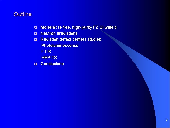
Effect of proton fluence on radiation defect structure of high-purity silicon for particle detectors Paweł Kamiński a, Roman Kozłowski a, Barbara Surma a, Michał Kozubal a Alexander Dierlamm b, Jerzy Krupka c, and Michał Kwestarz d a Institute of Electronic Materials Technology ul. Wólczyńska 133, 01 -919 Warszawa, Poland b Karlsruhe Institute of Technology, Hermann-von-Helmholtz Platz 1, 76 -344 Eggenstein-Leopoldshafen, Germany c Institute of Microelectronics and Optoelectronics, Warsaw University of Technology, ul. Koszykowa 75, 00 -662 Warszawa, Poland d Topsil Semiconductor Materials SA, ul. Wólczyńska 133, 01 -919 Warszawa, Poland 27 th RD 50 Workshop, 2 - 4 December 2015, CERN, Geneva 1

Outline q q Material: N-free, high-purity FZ Si wafers Neutron irradiations Radiation defect centers studies: Photoluminescence FTIR HRPITS Conclusions 2
![Material Orientation Type ρ300 K Ωcm 100 n 2200 200 P x 1012 cm3 Material Orientation Type ρ(300 K) [Ωcm] <100> n 2200± 200 [P] [x 1012 cm-3]](https://slidetodoc.com/presentation_image_h2/b7b7ff83ad16bfe5cb29a425941350cb/image-3.jpg)
Material Orientation Type ρ(300 K) [Ωcm] <100> n 2200± 200 [P] [x 1012 cm-3] [O] [x 1015 cm-3] [C] [x 1015 cm-3] [N] [x 1014 cm-3] ~2. 5 4 <5 <1 Electron mobility (300 K): ~ 1600 cm 2/Vs 3

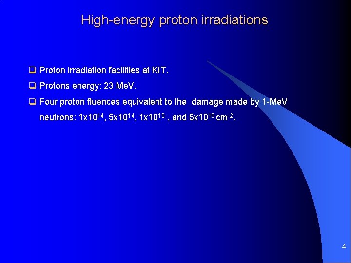
High-energy proton irradiations q Proton irradiation facilities at KIT. q Protons energy: 23 Me. V. q Four proton fluences equivalent to the damage made by 1 -Me. V neutrons: 1 x 10¹⁴, 5 x 10¹⁴, 1 x 10¹⁵ , and 5 x 1015 cm-2. 4

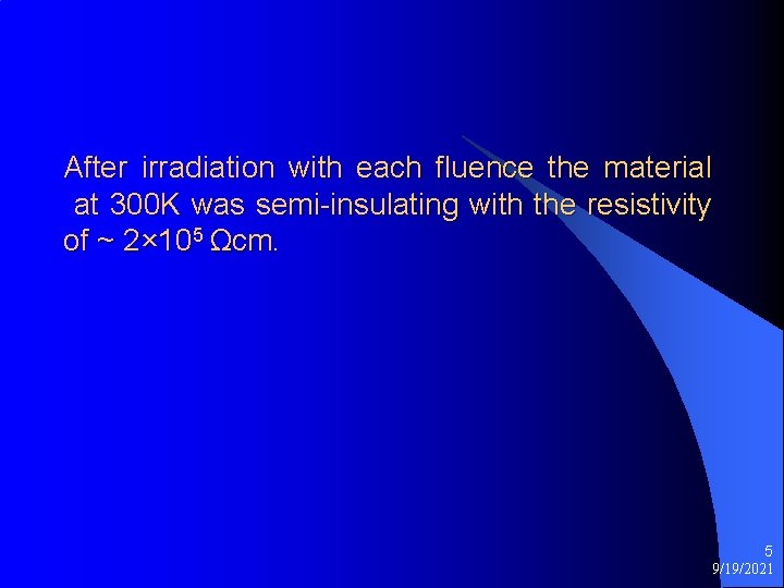
After irradiation with each fluence the material at 300 K was semi-insulating with the resistivity of ~ 2× 10⁵ Ωcm. 5 9/19/2021

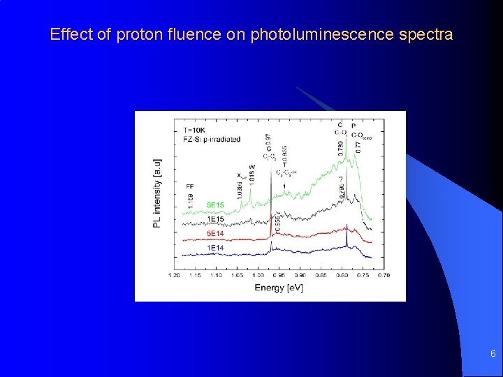
Effect of proton fluence on photoluminescence spectra 6

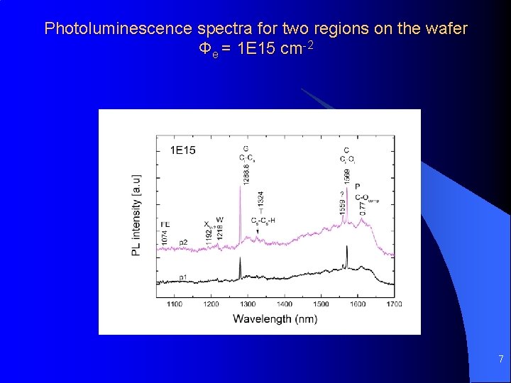
Photoluminescence spectra for two regions on the wafer Φe = 1 E 15 cm-2 7

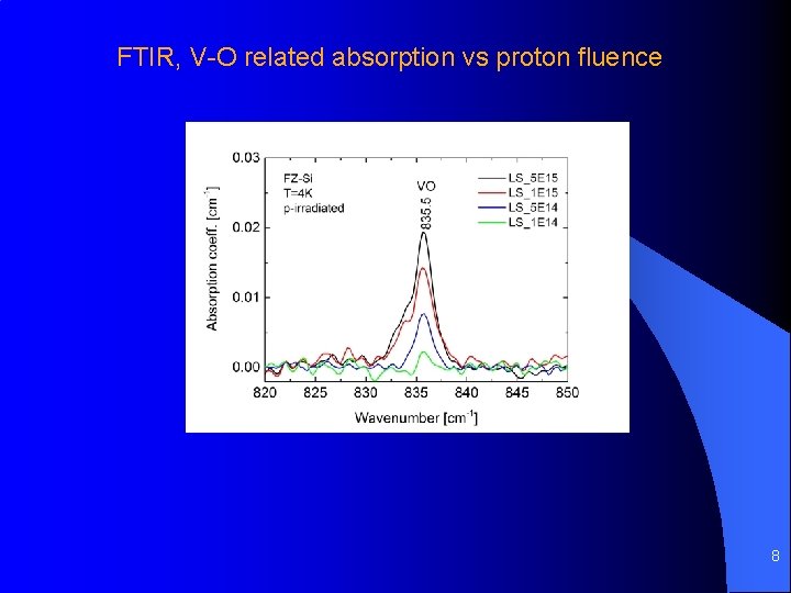
FTIR, V-O related absorption vs proton fluence 8

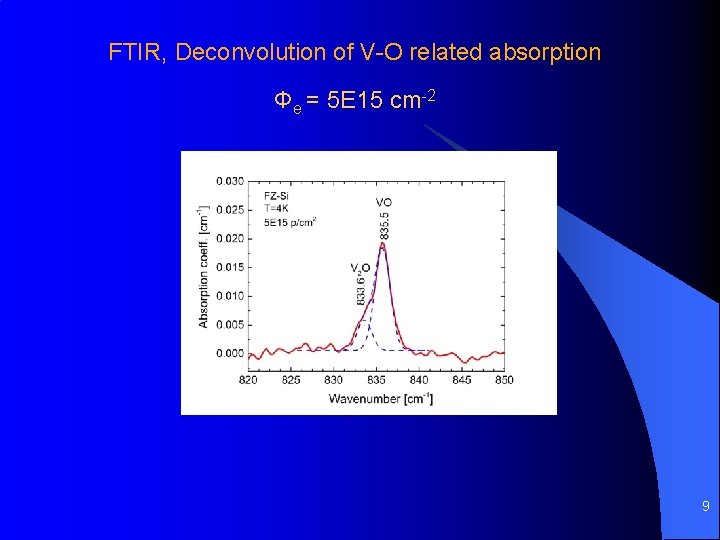
FTIR, Deconvolution of V-O related absorption Φe = 5 E 15 cm-2 9

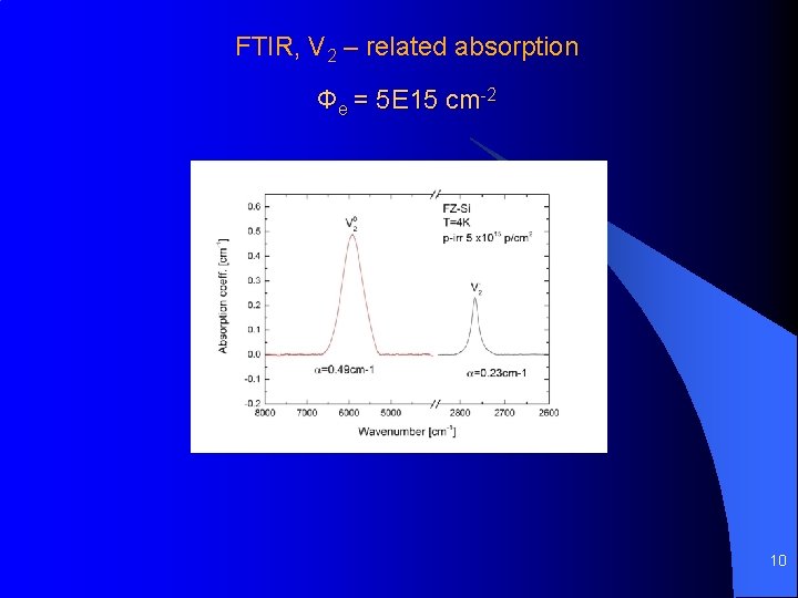
FTIR, V 2 – related absorption Φe = 5 E 15 cm-2 10
![FTIR V 2 concentration vs proton fluence Concentration cm3 1 0 E16 V FTIR, V 2 – concentration vs proton fluence Concentration [cm-3] 1, 0 E+16 V](https://slidetodoc.com/presentation_image_h2/b7b7ff83ad16bfe5cb29a425941350cb/image-11.jpg)
FTIR, V 2 – concentration vs proton fluence Concentration [cm-3] 1, 0 E+16 V 2 total 1, 0 E+15 V 20 1, 0 E+14 V 20 1, 0 E+13 V 21, 0 E+12 1 E+14 1 E+15 1 E+16 Proton fluence [p/cm 2] 11

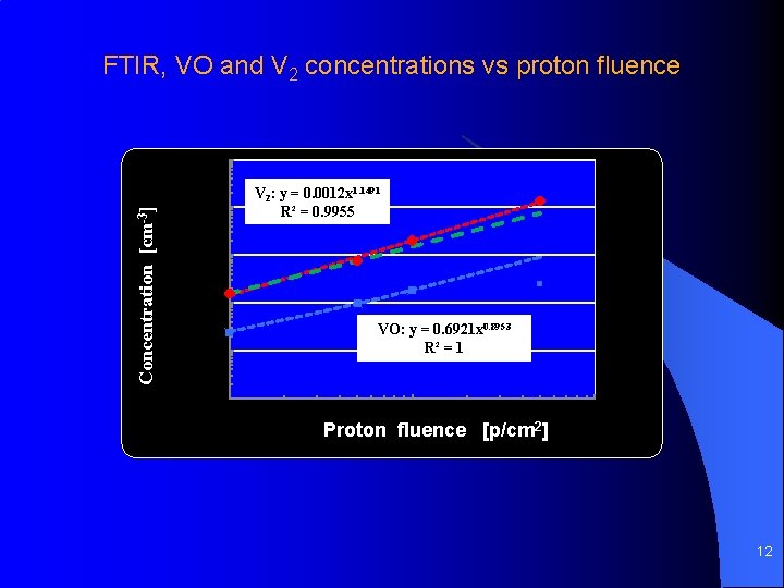
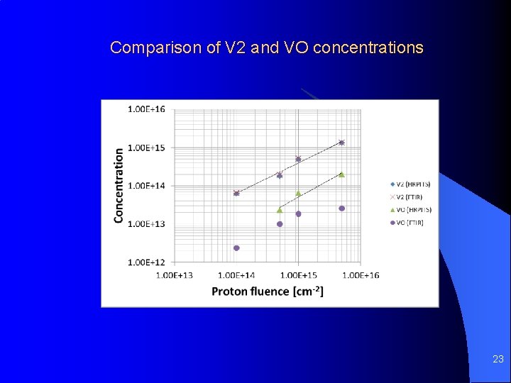
FTIR, VO and V 2 concentrations vs proton fluence 12

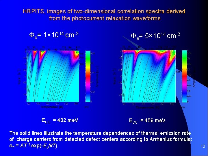
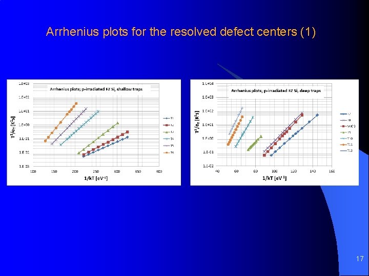
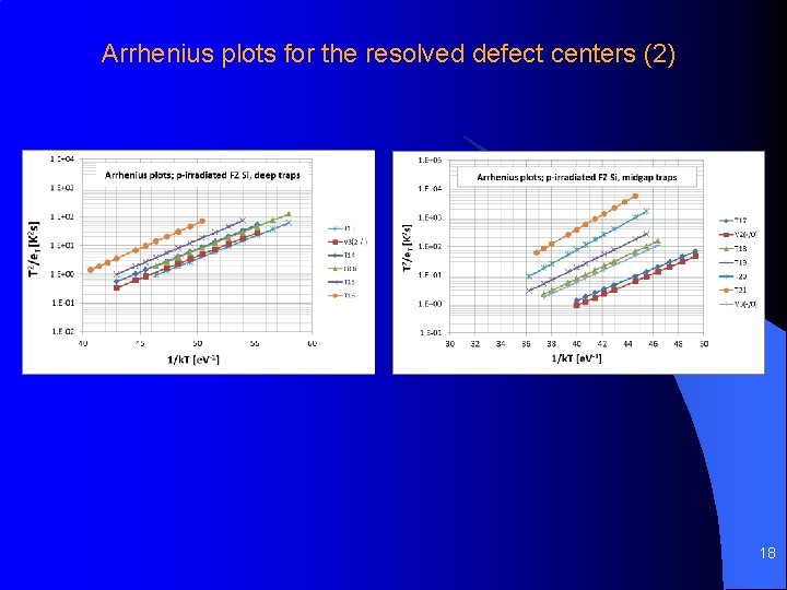
HRPITS, images of two-dimensional correlation spectra derived from the photocurrent relaxation waveforms Φe= 1× 1014 cm-3 EDC = 482 me. V Φe= 5× 1014 cm-3 EDC = 456 me. V The solid lines illustrate the temperature dependences of thermal emission rate of charge carriers from detected defect centers according to Arrhenius formula: e. T = AT 2 exp(-Ea/k. T). 13

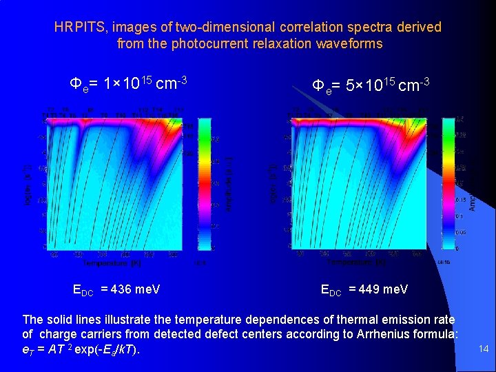
HRPITS, images of two-dimensional correlation spectra derived from the photocurrent relaxation waveforms Φe= 1× 1015 cm-3 EDC = 436 me. V Φe= 5× 1015 cm-3 EDC = 449 me. V The solid lines illustrate the temperature dependences of thermal emission rate of charge carriers from detected defect centers according to Arrhenius formula: e. T = AT 2 exp(-Ea/k. T). 14

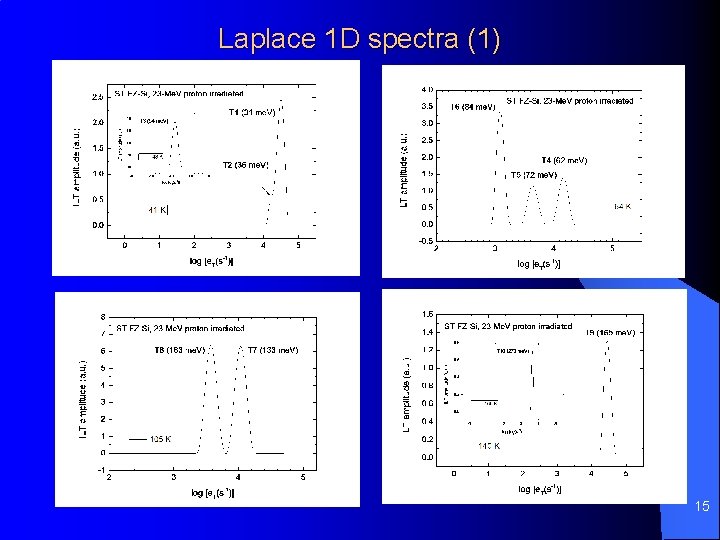
Laplace 1 D spectra (1) 15

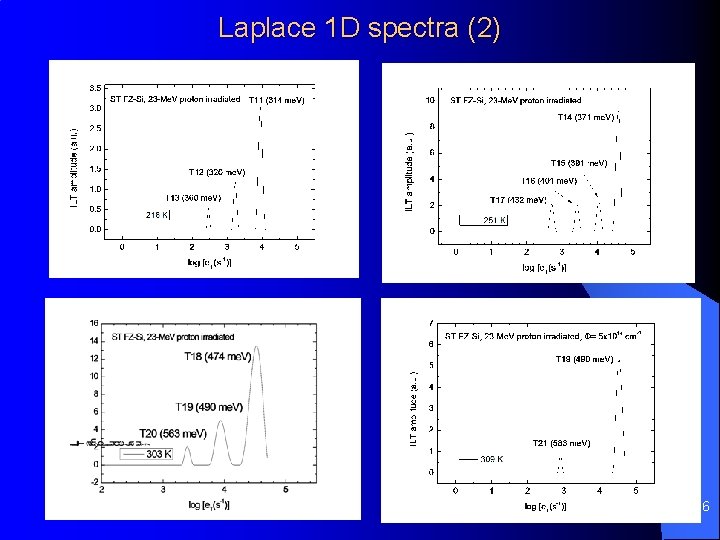
Laplace 1 D spectra (2) 16

Arrhenius plots for the resolved defect centers (1) 17

Arrhenius plots for the resolved defect centers (2) 18

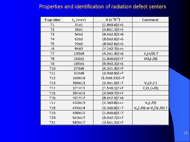
Properties and identification of radiation defect centers 19

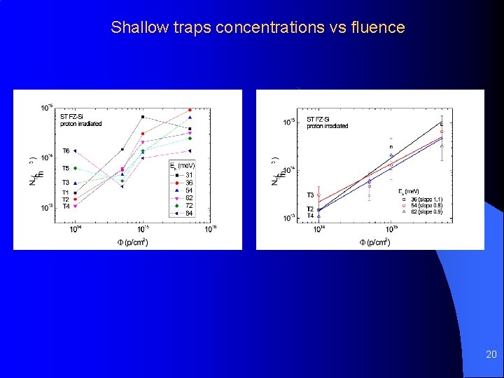
Shallow traps concentrations vs fluence 20

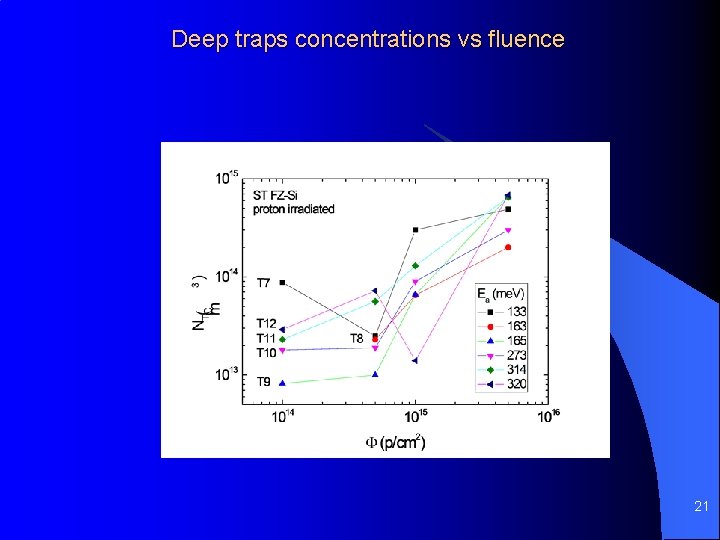
Deep traps concentrations vs fluence 21

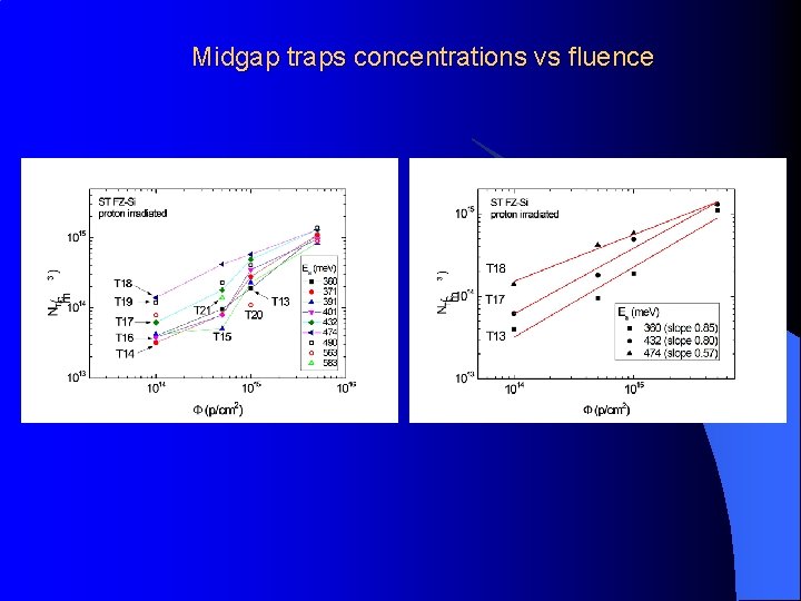
Midgap traps concentrations vs fluence

Comparison of V 2 and VO concentrations 23

Conclusions q We have demonstrated the effect of 23 -Me. V proton fluence on the properties and concentrations of electrically active radiation defect centers in detector grade, N-free, FZ Si with the resistivity of ~ 2000 Ωcm and low oxygen and carbon concentrations. q After the irradiation with the proton fluence equal or higher than 1 E 14 cm-2 the material becomes semi-insulating with the nearly intrinsic charge carriers concentrations. q The defect structure of the irradiated material is found to be complex. 21 irradiation-induced defect centers with activation energies of 30 – 590 me. V were detected. For the majority of centers there is nearly linear increase in the concentration with the fluence. q The divacancy concentration is found to be significantly higher than that of VO centers. 24

Acknowledgements This work has been partially supported by the National Centre for Research and Development within the framework of the Nitro. Sil project (ID: 208346) financed by the Program for Applied Research (Contract No. PBS 2 / A 9 / 26/2014). Thank you for your attention 25
![Concentration of VO defects Calibration factor VO6 1 x 10¹⁶ x a 300 K Concentration of VO defects Calibration factor [VO]*=6. 1 x 10¹⁶ x a 300 K](https://slidetodoc.com/presentation_image_h2/b7b7ff83ad16bfe5cb29a425941350cb/image-26.jpg)
Concentration of VO defects Calibration factor [VO]*=6. 1 x 10¹⁶ x a 300 K T=300 K FWHM=9 cm-1 a 4 K x FWHM 4 K = a 300 K x FWHM 300 K a 300 k was calculated *A. S. Oates & R. C. Newman Appl. Phys. Latt V 49 262 s (1986)
![Calibration factors V 2 5 5 x 1015 cm3 x a 2766 cm1 G Calibration factors [V 2 -]*=5. 5 x 1015 cm-3 x a (2766 cm-1) *G.](https://slidetodoc.com/presentation_image_h2/b7b7ff83ad16bfe5cb29a425941350cb/image-27.jpg)
Calibration factors [V 2 -]*=5. 5 x 1015 cm-3 x a (2766 cm-1) *G. Davies et all. Phys Rev B V 73, 165202, 2006 V 20=2. 99 x 1015 x S (5955 cm-1) S – integrated absorption where: N – concentration of defect (cm-3) f – oscillator strength = 0. 5 n – refraction index =3. 42 - absorption coefficient (cm-1) EF – photon energy (e. V)