Effect of Nano Structured Materials in High Speed


, Skin depth for carbon nano-materials (GNR,")
 and conductor loss: Conductance of graphene based")


![References [1]C. Xu, H. Li, and K. Banerjee, “Modeling, analysis and design of graphene](https://slidetodoc.com/presentation_image_h/318e1549c1b8fc0a19f45efec096edbc/image-13.jpg "References [1]C. Xu, H. Li, and K. Banerjee, “Modeling, analysis and design of graphene")

- Slides: 14
Effect of Nano Structured Materials in High Speed Digital Circuit Design Arin Dutta
Purpose of the Project : Ø Comparative study between Carbon Nano-materials and copper in high frequency digital circuit design. Ø Study of Electronic and thermal properties of Nano-materials in high frequency interconnect analysis and thermal analysis. Multilayer Armchair Graphene Nanoribbon (GNR) and Single Wall Carbon nanotube (SWCNT) has been considered for these analysis. Ø Finding a potential replacement of Traditional Interconnect and Thermal Vias Materials in high frequency digital circuit design.
Why Carbon Nano-materials in High Frequency Interconnect ? • conduct current densities orders of magnitude larger than copper wires [1]. • Electron mean free path in micron range [1]. • High Momentum Relaxation Time [2]. • Ballistic conduction [3]. • Superior thermal conductivity [4]. • Highly controllable in fabrication point of view [5].
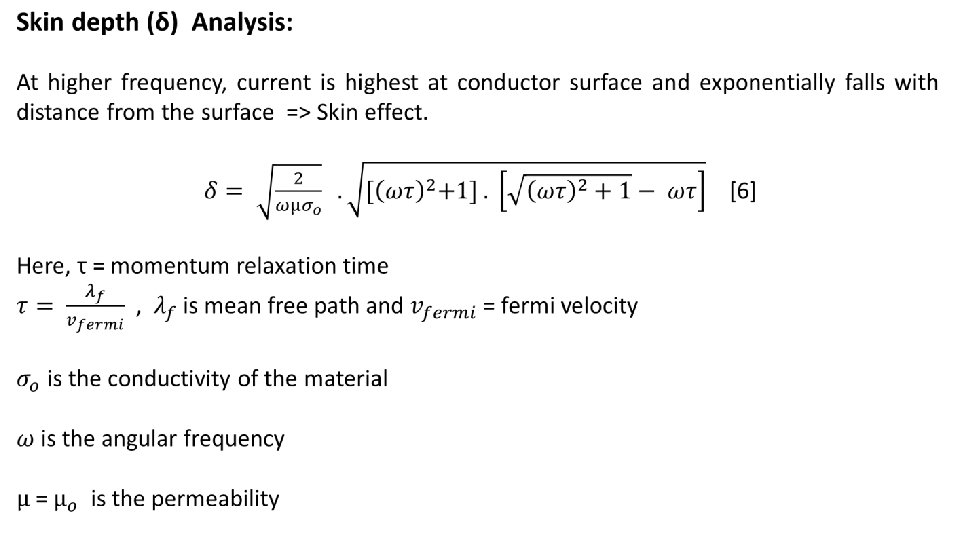
• At high frequency region (>100 GHz), Skin depth for carbon nano-materials (GNR, SWCNT) has been studied and compared with traditional interconnect material like Copper. 1 micron width and 1 meter length of the wire have been considered. • For copper wire, skin depth decreases continuously with frequency, but for both GNR and single wall CNT, skin depth decreases with frequency firstly and saturates at higher frequency region. • Ballistic conduction of nano-materials like GNR and SWCNT provide larger Mean free path and result larger scattering time (100 times) than copper which results a saturated skin depth at ultra high frequency indicating their promising applications in future high-frequency circuits Saturated Region
Analysis of Radio frequency sheet resistance (RFSR) and conductor loss: Conductance of graphene based nano-materials can be derived from Landauer formula and the equation of conductance [7] :
For wire having 1 meter length and 1 micron width and considering Fermi energy of 0. 21 e. V, the RFSR has been simulated for SWCNT and GNR and have been compared with traditional Copper Wire. • At room temperature, the larger mean free path provide larger electrical conductivity for SWCNT and GNR which results around 6 -7 times higher sheet conductivity for the SWCNT and GNR than that for Copper wire. So RFSR for SWCNT and GNR is lower than that for Copper wire at high frequency. • Conductor loss has been simulated and the higher RFSR increases the conductor loss of Copper wire than the carbon nano-material based wires.
Conductance of the nano-material based wire has been studied in terms of the wire width and compared with copper wire. The number of conduction channels in GNR and SWCNT is a function of wire width and as width increases, the number of conduction modes increases which enhances the conductance of GNR and SWCNT than Copper for varying width. Interlayer resistance for multilayer GNR is lower than the CNT and also the CNT diameter affects the conductance. Also for SWCNT, presence of only one shell add lower advantage in terms of conductivity than the GNR. So, for a particular width, the conductance for GNR is higher than the SWCNT.
The conductance of Nano-material based wires simulated in terms of Fermi Energy and compared with Copper baseline. • For lower fermi energy (<0. 1 e. V), due to less conduction channels, the conductance of SWCNT is nearer with copper baseline. • The each layer of the multilayer GNR provide conduction path which increases the conductance for GNR even at lower fermi energy. • At higher fermi energy (>0. 2 e. V), conductivity for both GNR and SWCNT becomes larger than Copper baseline
Thermal Analysis: • Ga. As die of 25 mils thickness bonded with LTCC 851 substrate containing thermal vias have been considered for study. • Carbon Nano-materials (GNR, SWCNT) have been considered as vias material and compared with Copper filled vias. • Thermal Resistance have been simulated in terms of via radius and number of vias. • The superior thermal conductivity of the carbon nanomaterials (10 times higher than copper [1]) makes thermal resistance lower than copper for varying vias radius and also vias number.
Thermal resistance is studied on different substrate materials : Alumina substrate and Diamond Substrate. Thickness of substrate has been considered 48 mils. The thermal resistance with carbon nanomaterials filled vias are compared with that for Copper. Due to the superior thermal conductivity for SWCNT and GNR, the package with carbon nano-materials filled vias have lower thermal resistance for all substrates than that of copper. Also, for substrate with high thermal conductivity like diamond, the package with SWCNT and GNR filled vias show uniform thermal resistance profile with varying number of vias.
Conclusion Ø At high frequency region, the carbon nano-material based interconnect wire lowers the skin effect by saturating the Skin depth. Ø The superior electrical conductance of carbon nano-materials lower the sheet resistance and conductor loss at High frequency region. Ø The higher thermal conductivity makes carbon nano-materials as potential candidate for thermal vias materials at High speed digital circuit applications by lowering thermal resistance. Ø For high speed digital circuit design, traditional materials like Copper can be replaced by carbon nano-materials like Carbon-nanotube and Graphene Nano-ribbon for their remarkable electronic and thermal properties.
References [1]C. Xu, H. Li, and K. Banerjee, “Modeling, analysis and design of graphene nano-ribbon interconnects, ” IEEE Trans. Electron Devices, vol. 56, no. 8, pp. 1567– 1578, Aug. 2009. [2] H. Li , C. Xu , N. Srivastava , K. Banerjee, “Carbon Nanomaterials for Next-Generation Interconnects and Passives: Physics, Status, and Prospects”, IEEE Trans. Electron Devices, vol. 56, no. 9, pp. 1799, Sept. 2009. [3] A. B Kaiser and V. Skakalova, “Electronic conduction in polymers, carbon nanotubes and graphene”, Chem. Soc. Rev. , vol. 40, pp. 3786– 3801, 2011. [4] S. Ghosh, I. Calizo, D. Teweldebrhan, E. Pokatilov, D. L. Nika, A. Balandin, W. Bao, F. Miao, and C. N. Lau, “Extremely high thermal conductivity of graphene: Prospects for thermal management applications in nanoelectronic circuits, ” Appl. Phys. Lett. , vol. 92, no. 15, p. 151 911, Apr. 2008. [5] M. Zeng, Y. Xiao, J. Liu, W. Lu, and L. Fu, “Controllable fabrication of nanostructured graphene towards electronics, ” Adv. Electron. Mater. 2, 1500456, 2016. [6] T. Nandy, A. Dutta, M. A. Haque and Z. H. Mahmood, “High frequency compatibility of doped multilayer graphene nanoribbon in VLSI interconnect with respect to skin depth effect and layer width variation”, Int. Conf. on Informatics, Electronics & Vision, pp. 1– 5, 2014. [7] C. Xu, H. Li, and K. Banerjee, “Graphene nano-ribbon (GNR) interconnects: A genuine contender or a delusive dream, ” IEDM Tech. Dig. , pp. 201– 204, 2008.
THANKS Q/A