Effect of Inversion layer Centroid on MOSFET capacitance



- Slides: 25

Effect of Inversion layer Centroid on MOSFET capacitance EEL 6935 class project Srivatsan Parthasarathy SWAMP Group

Organization • Introduction § Scaling Issues in nanometer MOSFETS § Parasitics – the ultimate showstoppers § Project relevance • Simulation Approach § Tools of the trade – what we need § Bandstructure § Self–consistent solution § Computing surface potential § Capacitance • Results and Discussion 1

Part I: Introduction

Scaling Issues in nanometer MOSFETS • Phenomenal scaling in last 40 years: § LGATE – from 10 μm to ~30 nm ! § Major changes in both technology and materials; • Smart optimizations in device structures • Timely introduction of new processing techniques • New materials (eg. Halo, silicides), but not in channel • Issues with scaling § Parasitics § Lesser control on Short Channel effects § Decreasing ION/IOFF (more leakage with thin oxide) § Industry is looking at new vectors § Strained Si, III-V channel materials, multi-gate architectures Part 1: Introduction 3

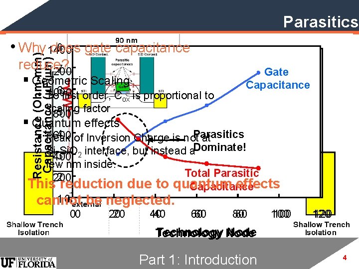
Parasitics Resistance (Ohm-mm) Capacitance (m. F/mm) 8 • Why 1400 does gate capacitance Channel reduce? 7 1200 Resistance Gate § Geometric Scaling Capacitance Series Resistance ~ 6 1000 • To first order, Cox is proportional to 47% of Channel Resistance scaling factor 5 800 § Quantum effects at 45 nm 4 of Inversion Charge is not Parasitics 600 • Peak at Dominate! Si-Si. O interface, but instead a Series 2 3 400 few nm inside. Resistance Total Parasitic 2 200 This reduction due to quantum effects Capacitance ITRS Roadmap 1 0 be neglected. cannot 20 40 60 80 100 120 00 20 40 60 80 100 120 Technology Node Technology Part 1: Introduction 4

Project relevance • Very important to quantify capacitance degradation § To build better device models and simulators § To compare how novel channel materials compete with existing technology Main goal of this project: § To quantify the quantum effects leading to reduction in capacitance using techniques taught in class Part 1: Introduction 5

What I did in the project • Simulated capacitance degradation for unstrained, planar n. MOS § Bandstructure - sp 3 d 5 s* TB model with SO coupling § Self-consistent solution of schroedinger-poisson equation § Surface potential calculation § Inversion Capacitance = d(QINV)/d(FS) • The TB Hamiltonian can be used 3 -5 materials also, but Ga. As or other materials was not simulated ( as initially planned) due to lack of time 6

Part II: Simulation Approach

Tools of the Trade • What all do we need? § Bulk bandstrcture • EMA, k • p, TB … which method to choose? • Trade-offs/Advantages in TB § Bandstrcture for M-O-S structure • Different from bulk bandstructure due to confinement § Self-consistent solution of schroedinger-poisson equations § Computing surface potential • How is FS related to VGATE ? Part 2: Approach 8

Bandstructure • Many approaches exist in theory § Single/multi-band Effective Mass Approximation (EMA) • Hartree, Hartree-Fock, Local Density Approximation § k • p method - based on the non-degenrate perturbation theory § Empirical and semi-empirical Tight Binding (TB) • sp 3 s*, sp 3 d 5 s* etc. § Density Functional Theory (DFT) Which method should I follow? Part 2: Approach 9

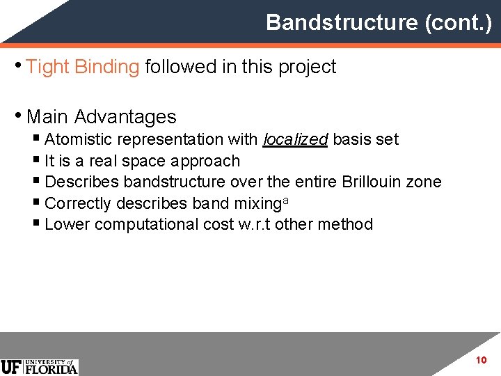
Bandstructure (cont. ) • Tight Binding followed in this project • Main Advantages § Atomistic representation with localized basis set § It is a real space approach § Describes bandstructure over the entire Brillouin zone § Correctly describes band mixinga § Lower computational cost w. r. t other method 10

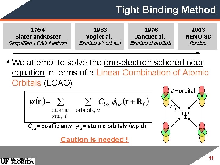
Tight Binding Method 1954 Slater and. Koster Simplified LCAO Method 1983 Vogl et al. Excited s* orbital 1998 Jancuet al. Excited d orbitals 2003 NEMO 3 D Purdue • We attempt to solve the one-electron schoredinger equation in terms of a Linear Combination of Atomic Orbitals (LCAO) f= orbital C ia Y Cia= coefficients fia= atomic orbitals (s, p, d) Caution is needed ! 11

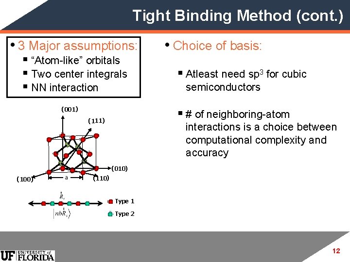
Tight Binding Method (cont. ) • 3 Major assumptions: § “Atom-like” orbitals § Two center integrals § NN interaction (001) • Choice of basis: § Atleast need sp 3 for cubic semiconductors § # of neighboring-atom (111) interactions is a choice between computational complexity and accuracy (010) (100) a (110) Type 1 Type 2 12

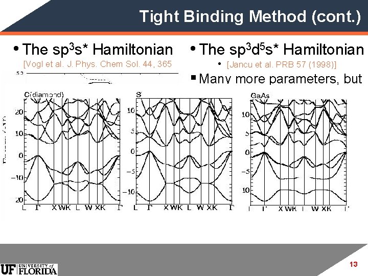
Tight Binding Method (cont. ) • The sp 3 s* Hamiltonian • The sp 3 d 5 s* Hamiltonian [Vogl et al. J. Phys. Chem Sol. 44, 365 (1983)] • In order to reproduce both valence and conduction band of covalently bounded semiconductors a s* orbital is introduced to account for high energy orbitals (d, f etc. ) • [Jancu et al. PRB 57 (1998)] § Many more parameters, but works quite well ! 13

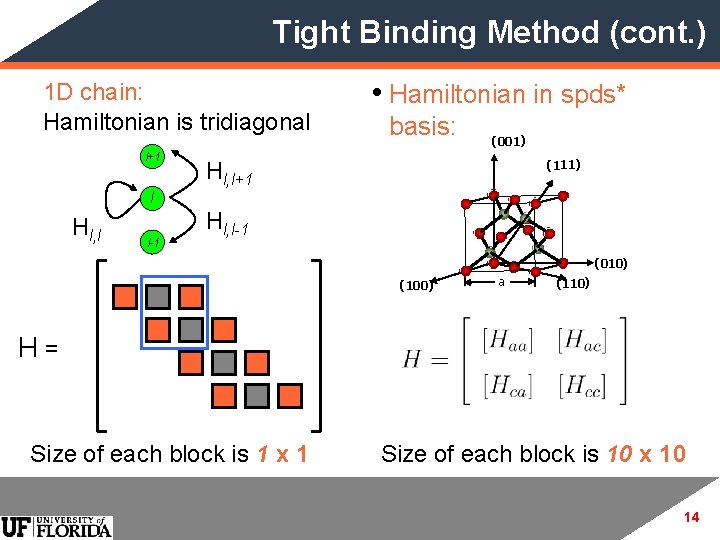
Tight Binding Method (cont. ) 1 D chain: Hamiltonian is tridiagonal l+1 • Hamiltonian in spds* basis: (001) Hl, l+1 (111) l Hl, l l-1 Hl, l-1 (010) (100) a (110) H= Size of each block is 1 x 1 Size of each block is 10 x 10 14

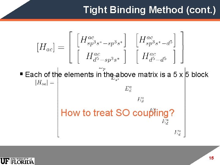
Tight Binding Method (cont. ) § Each of the elements in the above matrix is a 5 x 5 block How to treat SO coupling? 15

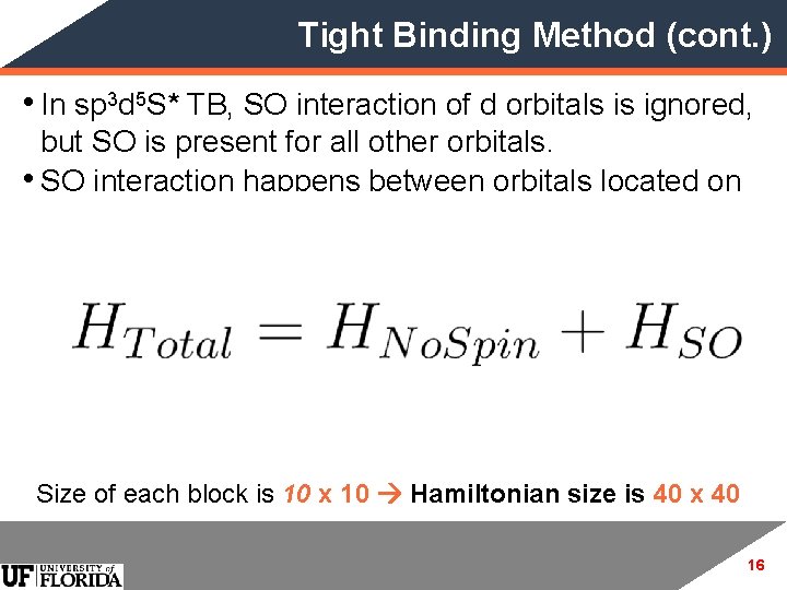
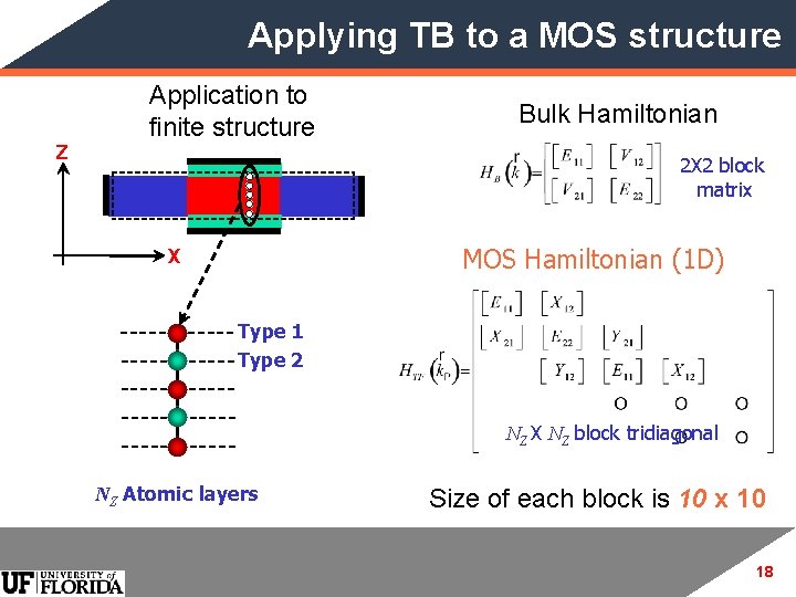
Tight Binding Method (cont. ) • In sp 3 d 5 S* TB, SO interaction of d orbitals is ignored, but SO is present for all other orbitals. • SO interaction happens between orbitals located on the same atom (not neighboring atoms). Size of each block is 10 x 10 Hamiltonian size is 40 x 40 16

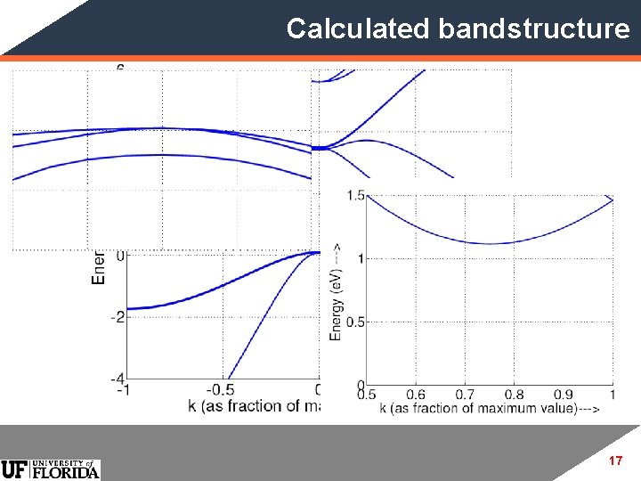
Calculated bandstructure 17

Applying TB to a MOS structure Z Application to finite structure Bulk Hamiltonian 2 X 2 block matrix MOS Hamiltonian (1 D) X Type 1 Type 2 NZ X NZ block tridiagonal NZ Atomic layers Size of each block is 10 x 10 18

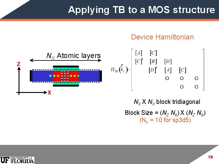
Applying TB to a MOS structure Device Hamiltonian Z NX Atomic layers X NX block tridiagonal Block Size = (NZ Nb) X (NZ Nb) (Nb = 10 for sp 3 d 5) 19

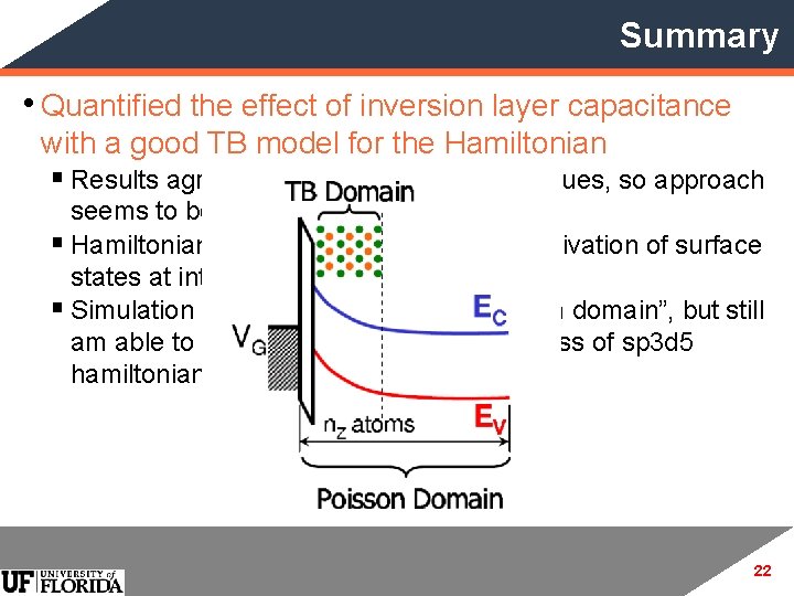
Capacitance Calculation • The schroedinger-poisson equation is solved selfconsistently using the method described in the text. • The total carrier concentration n(z) is calculated as a function of distance by summing up the electron concentration in each energy level. • For calculating the capacitance, we need to find surface potential at every gate voltage. § Ronald van Langevelde, "An explicit surface-potential-based MOSFET model for circuit simulation", Solid-State Electronics V 44 (2000) P 409 20

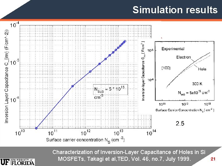
Simulation results Characterization of Inversion-Layer Capacitance of Holes in Si MOSFETs, Takagi et al, TED, Vol. 46, no. 7, July 1999. 21

Summary • Quantified the effect of inversion layer capacitance with a good TB model for the Hamiltonian § Results agreed with existing published values, so approach seems to be right. § Hamiltonian is not 100% accurate … passivation of surface states at interface, dangling bonds etc. § Simulation was only for a 15 nm “quantum domain”, but still am able to get good results effectiveness of sp 3 d 5 hamiltonian 22

References and Thanks • Exploring new channel materials for nanoscale CMOS devices: A simulation approach, Anisur Rahman, Ph. D Thesis, Purdue University, December 2005. • Dr. Yongke Sun, SWAMP Group, ECE – UF • Characterization of Inversion-Layer Capacitance • Guangyu Sun, SWAMP Group, ECE – UF of Holes in Si MOSFETs, Takagi et al, TED, Vol. 46, no. 7, July 1999. • Ronald van Langevelde, "An explicit surface-potential -based MOSFET model for circuit simulation", Solid. State Electronics V 44 (2000) P 409 23

Questions?