EET105 Fall 2018 Digital Electronics Charles Rubenstein Ph
EET-105 – Fall 2018 Digital Electronics Charles Rubenstein, Ph. D. Adjunct Professor of Engineering Session 10: WED 10/03/18 Mon/Wed: 9: 25 am – 11: 15 am // Wed/Fri: 11: 40 am – 1: 30 pm Lupton Hall 247
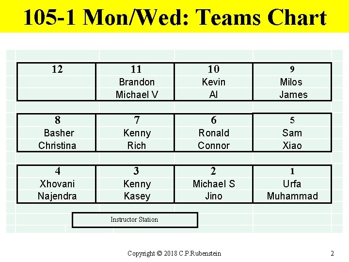
105 -1 Mon/Wed: Teams Chart 12 11 10 Brandon Michael V Kevin Al 9 Milos James 7 6 Basher Christina Kenny Rich Ronald Connor 5 Sam Xiao 4 3 2 Xhovani Najendra Kenny Kasey Michael S Jino 1 Urfa Muhammad Instructor Station Copyright © 2018 C. P. Rubenstein 8 2
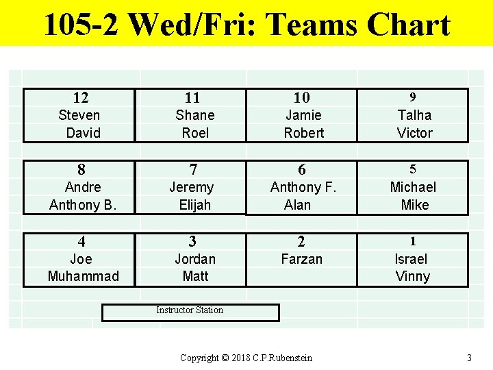
105 -2 Wed/Fri: Teams Chart 12 11 10 Steven David Shane Roel Jamie Robert 9 Talha Victor 7 6 Andre Anthony B. Jeremy Elijah Anthony F. Alan 5 Michael Mike 4 3 2 Joe Muhammad Jordan Matt Farzan 1 Israel Vinny Instructor Station Copyright © 2018 C. P. Rubenstein 8 3
Instructor Contact Information Dr. Charles Rubenstein <c. rubenstein@ieee. org> Adjunct Professor of Engineering Office hours (by appointment *) in LH 247 Mon: 9: 00 am – 9: 20 am Wed: 9: 00 am – 9: 20 am Fri: 11: 00 am – 11: 30 am (*Please email me at least a day in advance if you plan on coming to office hours…) Send me an email … Subject line: 105 Copyright © 2018 C. P. Rubenstein 4
Class Session Archives http: //www. Charles. Rubenstein. com/105/ 18 fa 10. pdf (Class Power. Point slides) * 18 fa 10_h. pdf (slides in handout format) * *Archive materials are normally online four days after class Copyright © 2018 C. P. Rubenstein 5
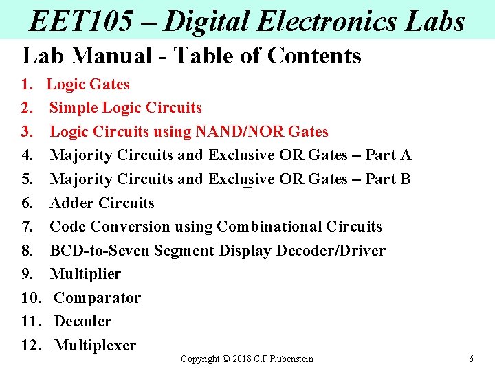
EET 105 – Digital Electronics Lab Manual - Table of Contents 1. Logic Gates 2. Simple Logic Circuits 3. Logic Circuits using NAND/NOR Gates 4. Majority Circuits and Exclusive OR Gates – Part A 5. Majority Circuits and Exclusive OR Gates – Part B – 6. Adder Circuits 7. Code Conversion using Combinational Circuits 8. BCD-to-Seven Segment Display Decoder/Driver 9. Multiplier 10. Comparator 11. Decoder 12. Multiplexer Copyright © 2018 C. P. Rubenstein 6
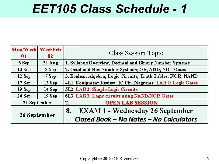
EET 105 Class Schedule - 1 Mon/Wed: Wed/Fri: 01 02 5 Sep 31 Aug 10 Sep 5 Sep 12 Sep 7 Sep 12 Sep 19 Sep 14 Sep 24 Sep 19 Sep 21 September 26 September Class Session Topic 1. Syllabus Overview, Decimal and Binary Number Systems 2. Octal and Hex Number Systems; OR, AND, NOT Gates 3. Boolean Algebra; Logic Circuits; Truth Tables; NOR, NAND 4 L 1. Equipment Review; IC Pin Diagrams; LAB 1: Logic Gates –– 5 L 2. LAB 2: Simple Logic Circuits 6 L 3. LAB 3: Logic circuits using NAND/NOR Gates 7. OPEN LAB SESSION 8. EXAM 1 - Wednesday 26 September Closed Book – No Notes – No Calculators Copyright © 2018 C. P. Rubenstein 7
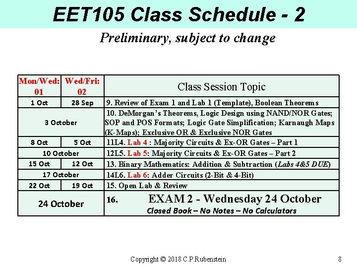
EET 105 Class Schedule - 2 Preliminary, subject to change Mon/Wed: Wed/Fri: 01 02 1 Oct 28 Sep 3 October 8 Oct 5 Oct 10 October 15 Oct 12 Oct 17 October 22 Oct 19 Oct 24 October Class Session Topic 9. Review of Exam 1 and Lab 1 (Template), Boolean Theorems 10. De. Morgan’s Theorems, Logic Design using NAND/NOR Gates; SOP and POS Formats; Logic Gate Simplification; Karnaugh Maps (K-Maps); Exclusive OR & Exclusive NOR Gates 11 L 4. Lab 4 : Majority Circuits & Ex-OR Gates – Part 1 12 L 5. Lab 5: Majority Circuits & Ex-OR Gates – Part 2 13. Binary Mathematics: Addition & Subtraction (Labs 4&5 DUE) 14 L 6. Lab 6: Adder Circuits (2 -Bit & 4 -Bit) 15. Open Lab & Review 16. EXAM 2 - Wednesday 24 October Closed Book – No Notes – No Calculators Copyright © 2018 C. P. Rubenstein 8
In Today’s Class: • Due: Lab Reports 2 and 3 • Lecture: Boolean & De. Morgan’s Theorems Logic Design using NAND/NOR Gates SOP and POS Formats Logic Gate Simplification Karnaugh Maps (K-Maps) Exclusive OR & Exclusive NOR Gates Next Class: Lab 4 : Majority Circuits & Ex-OR Gates – Part 1 Copyright © 2018 C. P. Rubenstein 10

Questions? Copyright © 2018 C. P. Rubenstein 11
MORE Boolean Theorems Copyright © 2018 C. P. Rubenstein 12
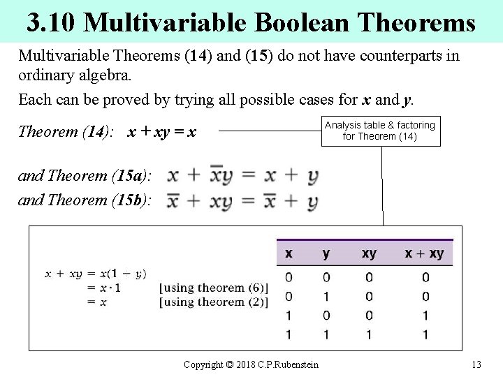
3. 10 Multivariable Boolean Theorems Multivariable Theorems (14) and (15) do not have counterparts in ordinary algebra. Each can be proved by trying all possible cases for x and y. Theorem (14): x + xy = x Analysis table & factoring for Theorem (14) and Theorem (15 a): and Theorem (15 b): Copyright © 2018 C. P. Rubenstein 13
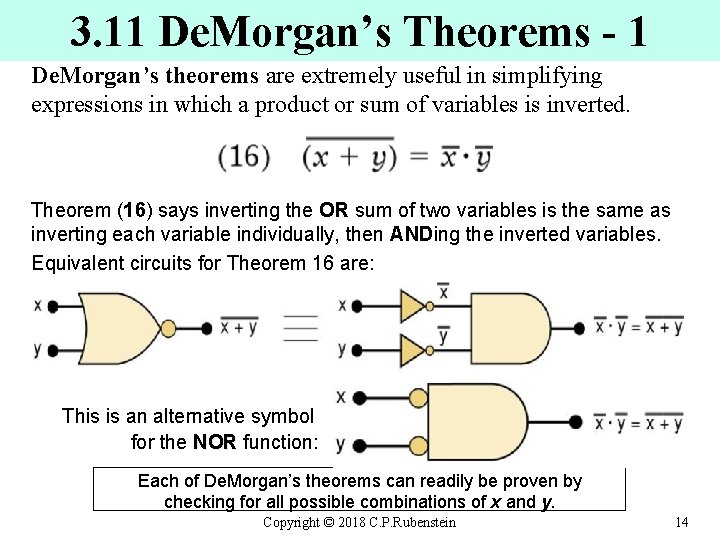
3. 11 De. Morgan’s Theorems - 1 De. Morgan’s theorems are extremely useful in simplifying expressions in which a product or sum of variables is inverted. Theorem (16) says inverting the OR sum of two variables is the same as inverting each variable individually, then ANDing the inverted variables. Equivalent circuits for Theorem 16 are: This is an alternative symbol for the NOR function: NOR Each of De. Morgan’s theorems can readily be proven by checking for all possible combinations of x and y. Copyright © 2018 C. P. Rubenstein 14
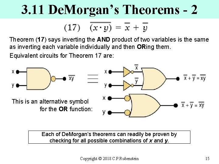
3. 11 De. Morgan’s Theorems - 2 Theorem (17) says inverting the AND product of two variables is the same as inverting each variable individually and then ORing them. Equivalent circuits for Theorem 17 are: This is an alternative symbol for the OR function: OR Each of De. Morgan’s theorems can readily be proven by checking for all possible combinations of x and y. Copyright © 2018 C. P. Rubenstein 15
3. 12 Universality of NAND & NOR Gates - 1 We already studied that NAND or NAND NOR gates can NOR be used to create three basic logic expressions: OR, OR AND, and INVERT (NOT). AND Using only NAND or NOR gates provides flexibility and is very useful in logic circuit design as can be seen on the next slide Copyright © 2018 C. P. Rubenstein 16
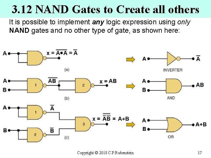
3. 12 NAND Gates to Create all others It is possible to implement any logic expression using only NAND gates and no other type of gate, as shown here: Copyright © 2018 C. P. Rubenstein 17
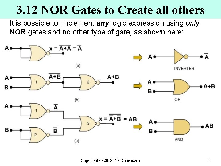
3. 12 NOR Gates to Create all others It is possible to implement any logic expression using only NOR gates and no other type of gate, as shown here: Copyright © 2018 C. P. Rubenstein 18
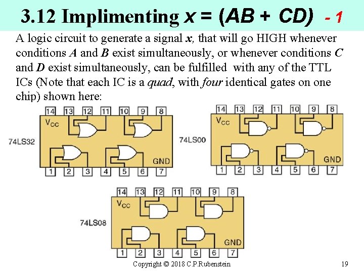
3. 12 Implimenting x = (AB + CD) -1 A logic circuit to generate a signal x, that will go HIGH whenever conditions A and B exist simultaneously, or whenever conditions C and D exist simultaneously, can be fulfilled with any of the TTL ICs (Note that each IC is a quad, with four identical gates on one chip) shown here: Copyright © 2018 C. P. Rubenstein 19
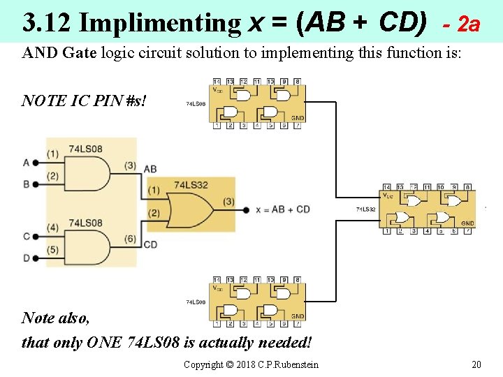
3. 12 Implimenting x = (AB + CD) - 2 a AND Gate logic circuit solution to implementing this function is: NOTE IC PIN #s! Note also, that only ONE 74 LS 08 is actually needed! Copyright © 2018 C. P. Rubenstein 20
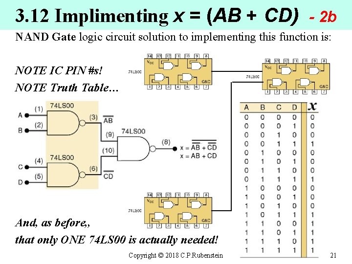
3. 12 Implimenting x = (AB + CD) - 2 b NAND Gate logic circuit solution to implementing this function is: NOTE IC PIN #s! NOTE Truth Table… And, as before, , that only ONE 74 LS 00 is actually needed! Copyright © 2018 C. P. Rubenstein 21
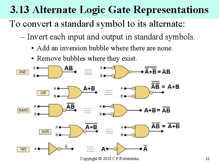
3. 13 Alternate Logic Gate Representations To convert a standard symbol to its alternate: – Invert each input and output in standard symbols. • Add an inversion bubble where there are none. • Remove bubbles where they exist. Copyright © 2018 C. P. Rubenstein 22
Chapter 4 Simplifying Logic Circuits Copyright © 2018 C. P. Rubenstein 23
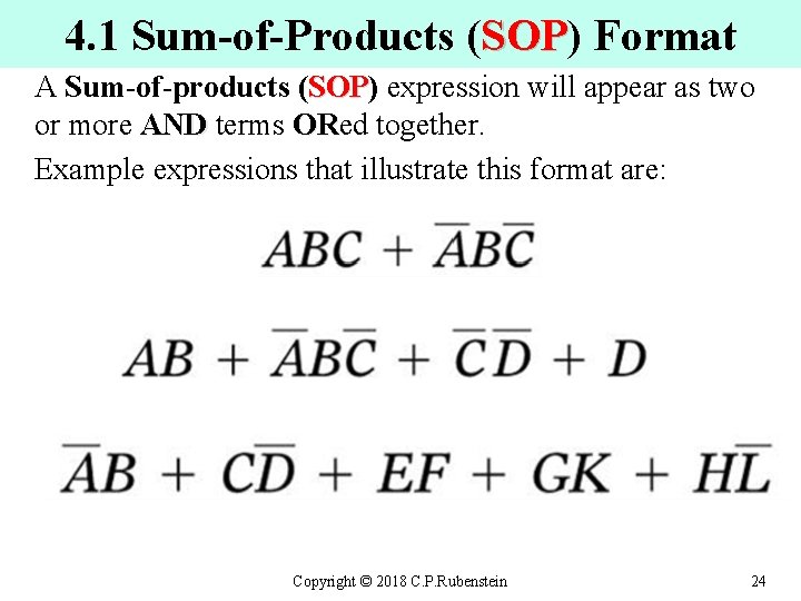
4. 1 Sum-of-Products (SOP) Format SOP A Sum-of-products (SOP) expression will appear as two SOP or more AND terms ORed together. AND OR Example expressions that illustrate this format are: Copyright © 2018 C. P. Rubenstein 24
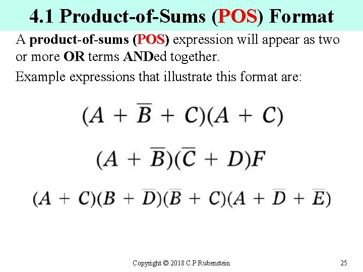
4. 1 Product-of-Sums (POS) Format POS A product-of-sums (POS) expression will appear as two POS or more OR terms ANDed together. OR AND Example expressions that illustrate this format are: Copyright © 2018 C. P. Rubenstein 25
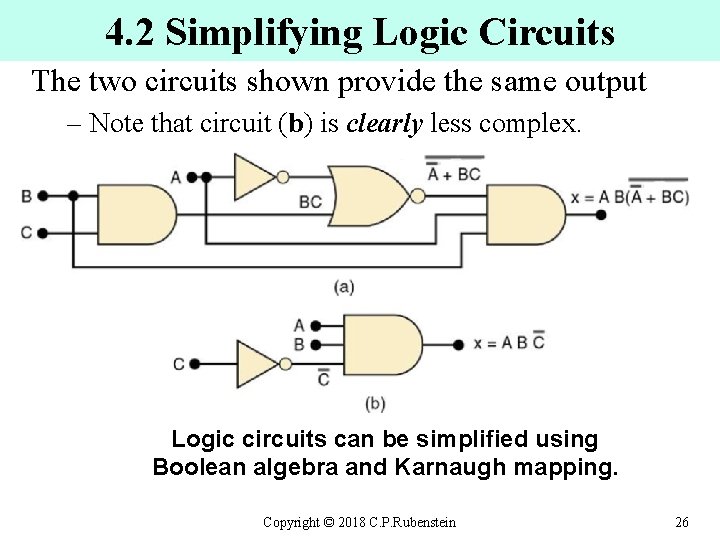
4. 2 Simplifying Logic Circuits The two circuits shown provide the same output – Note that circuit (b) is clearly less complex. Logic circuits can be simplified using Boolean algebra and Karnaugh mapping. Copyright © 2018 C. P. Rubenstein 26
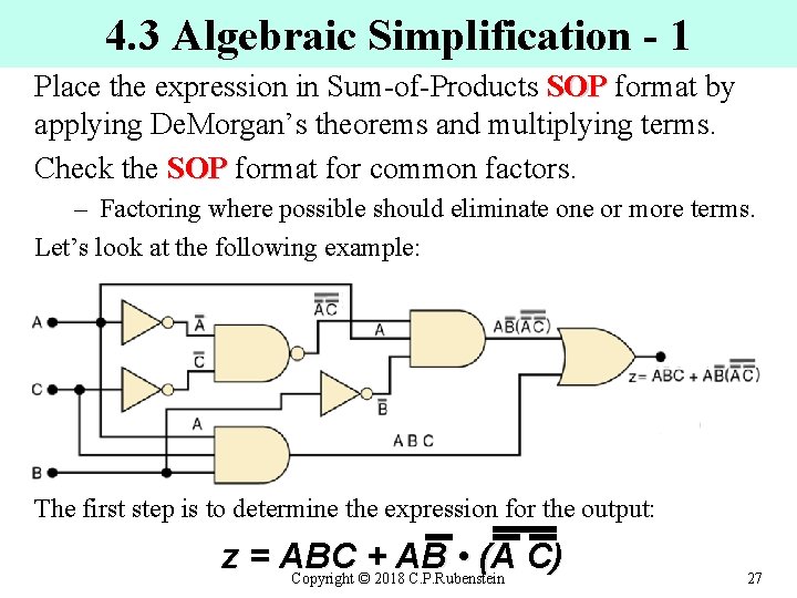
4. 3 Algebraic Simplification - 1 Place the expression in Sum-of-Products SOP format by SOP applying De. Morgan’s theorems and multiplying terms. Check the SOP format for common factors. SOP – Factoring where possible should eliminate one or more terms. Let’s look at the following example: The first step is to determine the expression for the output: z = ABC + AB • (A C) Copyright © 2018 C. P. Rubenstein 27
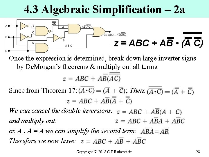
4. 3 Algebraic Simplification – 2 a z = ABC + AB • (A C) Once the expression is determined, break down large inverter signs by De. Morgan’s theorems & multiply out all terms: Since from Theorem 17: ; Then: We cancel the double inversions: and multiply out: as A ● A = A we can simplify the second term: Therefore we now have: Copyright © 2018 C. P. Rubenstein 28
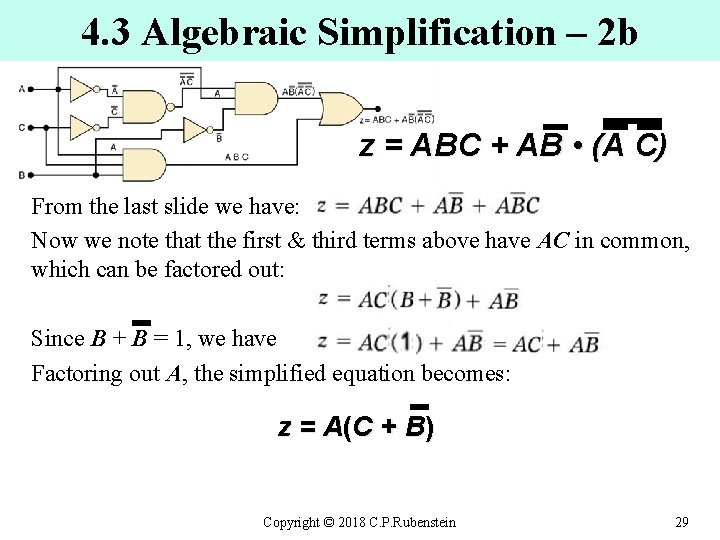
4. 3 Algebraic Simplification – 2 b z = ABC + AB • (A C) From the last slide we have: Now we note that the first & third terms above have AC in common, which can be factored out: Since B + B = 1, we have Factoring out A, the simplified equation becomes: z = A (C + B ) Copyright © 2018 C. P. Rubenstein 29
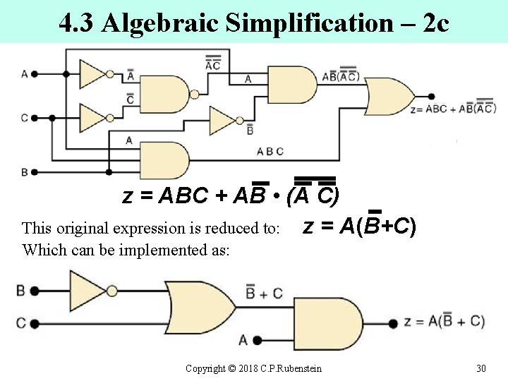
4. 3 Algebraic Simplification – 2 c z = ABC + AB • (A C) This original expression is reduced to: z = A(B+C) Which can be implemented as: Copyright © 2018 C. P. Rubenstein 30
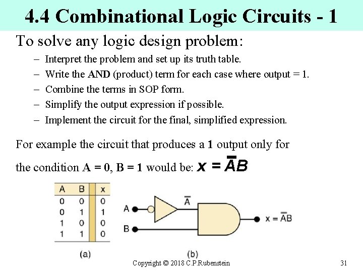
4. 4 Combinational Logic Circuits - 1 To solve any logic design problem: – – – Interpret the problem and set up its truth table. Write the AND (product) term for each case where output = 1. AND Combine the terms in SOP form. Simplify the output expression if possible. Implement the circuit for the final, simplified expression. For example the circuit that produces a 1 output only for the condition A = 0, B = 1 would be: x = AB Copyright © 2018 C. P. Rubenstein 31
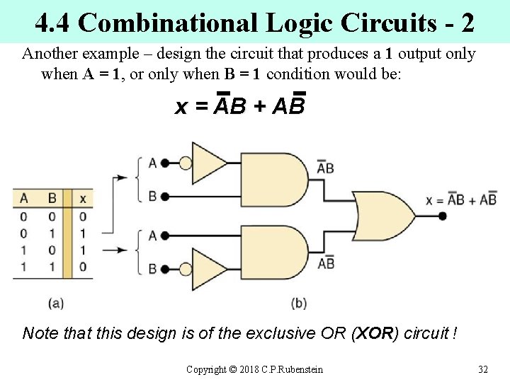
4. 4 Combinational Logic Circuits - 2 Another example – design the circuit that produces a 1 output only when A = 1, or only when B = 1 condition would be: x = AB + AB Note that this design is of the exclusive OR (XOR) circuit ! Copyright © 2018 C. P. Rubenstein 32
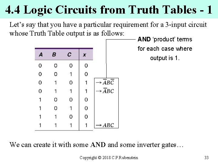
4. 4 Logic Circuits from Truth Tables - 1 Let’s say that you have a particular requirement for a 3 -input circuit whose Truth Table output is as follows: AND ‘product’ terms AND for each case where output is 1. We can create it with some AND and some inverter gates… Copyright © 2018 C. P. Rubenstein 33
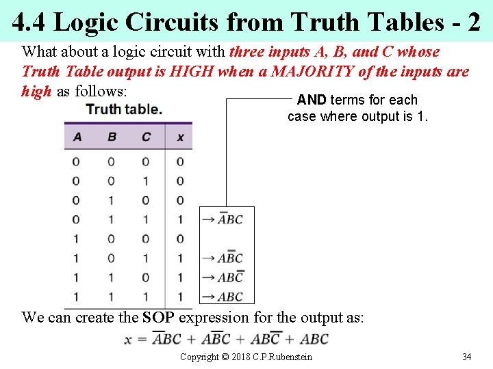
4. 4 Logic Circuits from Truth Tables - 2 What about a logic circuit with three inputs A, B, and C whose Truth Table output is HIGH when a MAJORITY of the inputs are high as follows: AND terms for each AND case where output is 1. We can create the SOP expression for the output as: Copyright © 2018 C. P. Rubenstein 34
Chapter 4 Karnaugh Maps (K-Maps) Copyright © 2018 C. P. Rubenstein 35
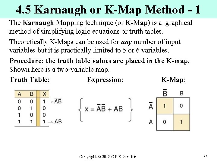
4. 5 Karnaugh or K-Map Method - 1 The Karnaugh Mapping technique (or K-Map) is a graphical method of simplifying logic equations or truth tables. Theoretically K-Maps can be used for any number of input variables but it is practically limited to 5 or 6 variables. Procedure: the truth table values are placed in the K-map. Shown here is a two-variable map. Truth Table: Expression: K-Map: Copyright © 2018 C. P. Rubenstein 36
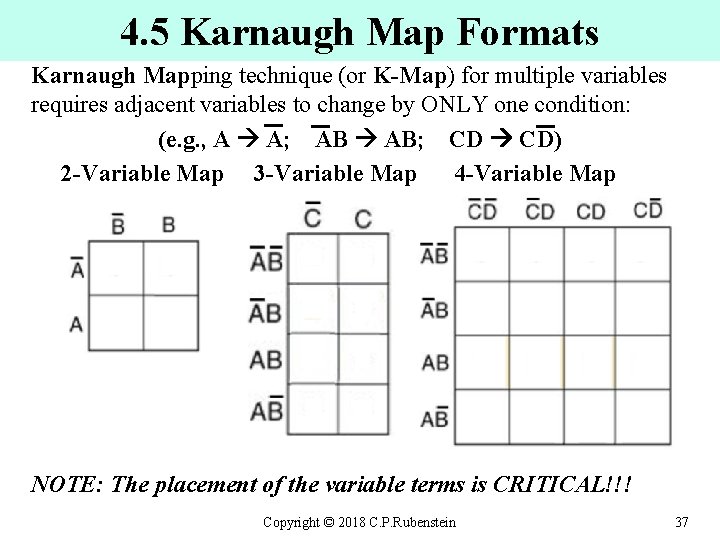
4. 5 Karnaugh Map Formats Karnaugh Mapping technique (or K-Map) for multiple variables requires adjacent variables to change by ONLY one condition: (e. g. , A A; AB AB; CD CD) 2 -Variable Map 3 -Variable Map 4 -Variable Map NOTE: The placement of the variable terms is CRITICAL!!! Copyright © 2018 C. P. Rubenstein 37
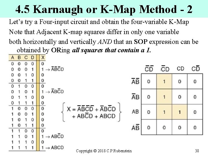
4. 5 Karnaugh or K-Map Method - 2 Let’s try a Four-input circuit and obtain the four-variable K-Map Note that Adjacent K-map squares differ in only one variable both horizontally and vertically AND that an SOP expression can be obtained by ORing all squares that contain a 1. OR Copyright © 2018 C. P. Rubenstein 38
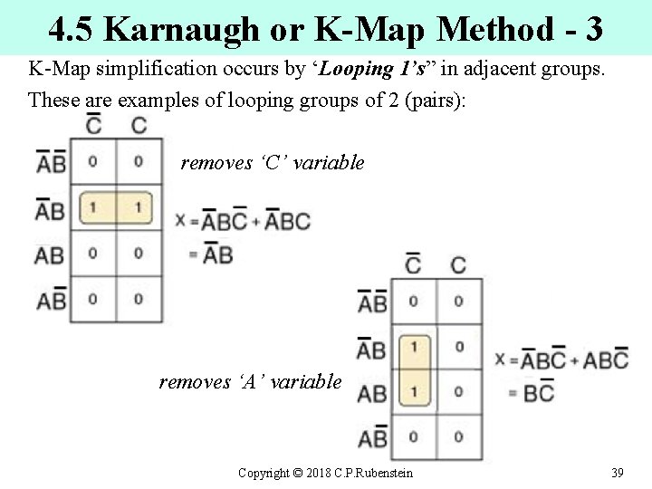
4. 5 Karnaugh or K-Map Method - 3 K-Map simplification occurs by ‘Looping 1’s” in adjacent groups. These are examples of looping groups of 2 (pairs): removes ‘C’ variable removes ‘A’ variable Copyright © 2018 C. P. Rubenstein 39
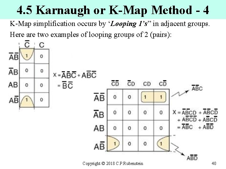
4. 5 Karnaugh or K-Map Method - 4 K-Map simplification occurs by ‘Looping 1’s” in adjacent groups. Here are two examples of looping groups of 2 (pairs): Copyright © 2018 C. P. Rubenstein 40
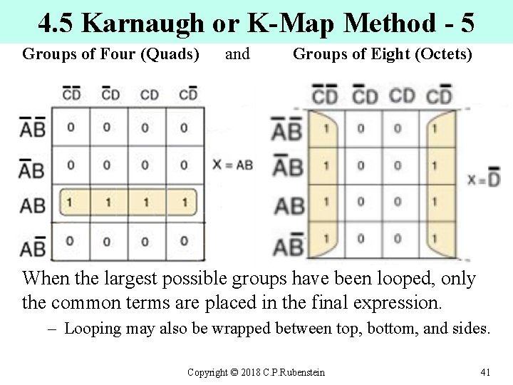
4. 5 Karnaugh or K-Map Method - 5 Groups of Four (Quads) and Groups of Eight (Octets) When the largest possible groups have been looped, only the common terms are placed in the final expression. – Looping may also be wrapped between top, bottom, and sides. Copyright © 2018 C. P. Rubenstein 41
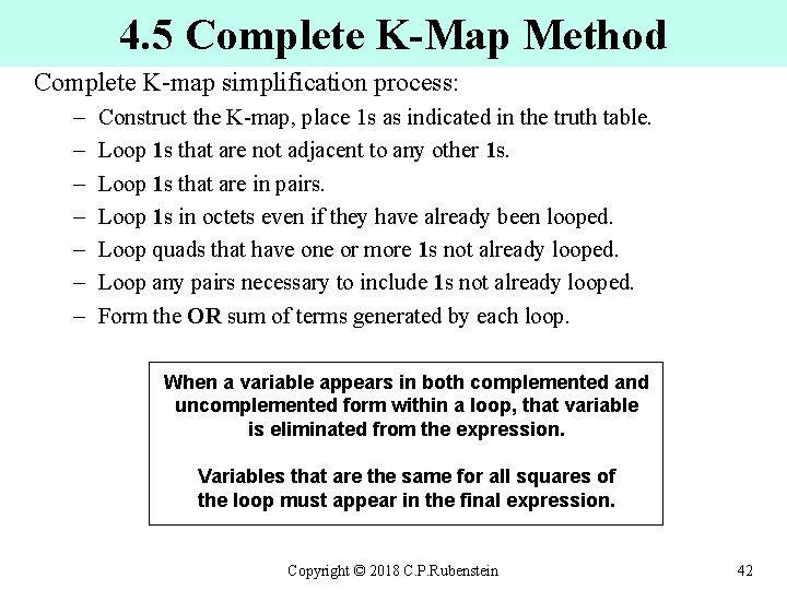
4. 5 Complete K-Map Method Complete K-map simplification process: – – – – Construct the K-map, place 1 s as indicated in the truth table. Loop 1 s that are not adjacent to any other 1 s. Loop 1 s that are in pairs. Loop 1 s in octets even if they have already been looped. Loop quads that have one or more 1 s not already looped. Loop any pairs necessary to include 1 s not already looped. Form the OR sum of terms generated by each loop. OR When a variable appears in both complemented and uncomplemented form within a loop, that variable is eliminated from the expression. Variables that are the same for all squares of the loop must appear in the final expression. Copyright © 2018 C. P. Rubenstein 42
Chapter 4 Exclusive OR / Ex-NOR Circuits Copyright © 2018 C. P. Rubenstein 43
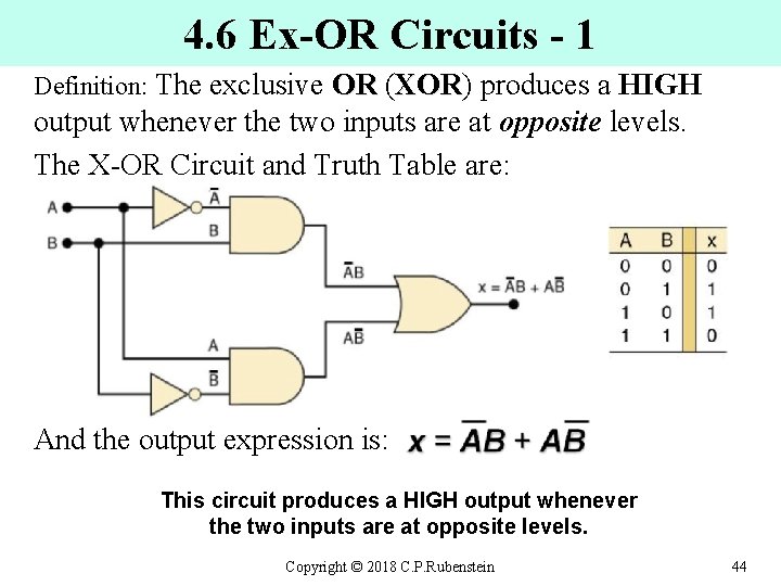
4. 6 Ex-OR Circuits - 1 Definition: The exclusive OR ( OR XOR) produces a HIGH XOR output whenever the two inputs are at opposite levels. The X-OR Circuit and Truth Table are: And the output expression is: This circuit produces a HIGH output whenever the two inputs are at opposite levels. Copyright © 2018 C. P. Rubenstein 44
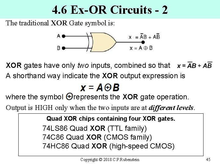
4. 6 Ex-OR Circuits - 2 The traditional XOR Gate symbol is: XOR gates have only two inputs, combined so that XOR A shorthand way indicate the XOR output expression is XOR where the symbol represents the XOR gate operation. XOR Output is HIGH only when the two inputs are at different levels. Quad XOR chips containing four XOR gates. 74 LS 86 Quad XOR (TTL family) XOR 74 C 86 Quad XOR (CMOS family) XOR 74 HC 86 Quad XOR (high-speed CMOS) XOR Copyright © 2018 C. P. Rubenstein 45
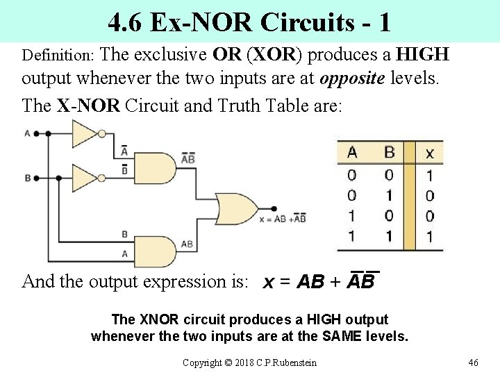
4. 6 Ex-NOR Circuits - 1 Definition: The exclusive OR ( OR XOR) produces a HIGH XOR output whenever the two inputs are at opposite levels. The X-NOR Circuit and Truth Table are: And the output expression is: x = AB + AB The XNOR circuit produces a HIGH output whenever the two inputs are at the SAME levels. Copyright © 2018 C. P. Rubenstein 46
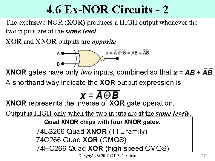
4. 6 Ex-NOR Circuits - 2 The exclusive NOR (XOR) produces a HIGH output whenever the two inputs are at the same level. XOR and XNOR outputs are opposite. XNOR gates have only two inputs, combined so that XNOR A shorthand way indicate the XOR output expression is XOR XNOR represents the inverse of XOR gate operation. XOR Output is HIGH only when the two inputs are at the same levels. Quad XNOR chips with four XNOR gates. 74 LS 266 Quad XNOR (TTL family) XNOR 74 C 266 Quad XOR (CMOS) XOR 74 HC 266 Quad XOR (high-speed CMOS) XOR Copyright © 2018 C. P. Rubenstein 47
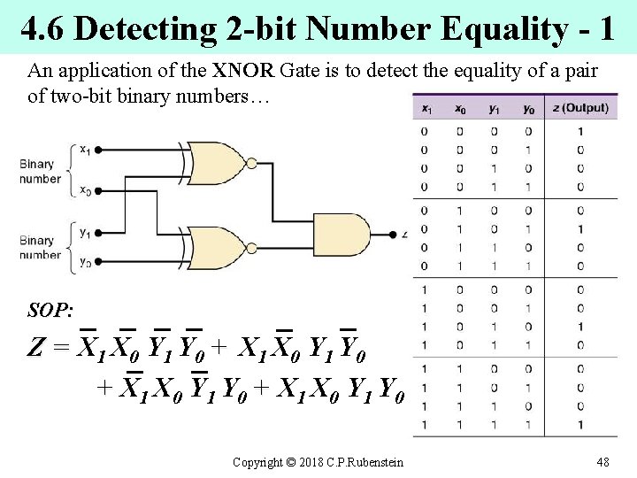
4. 6 Detecting 2 -bit Number Equality - 1 An application of the XNOR Gate is to detect the equality of a pair of two-bit binary numbers… SOP: Z = X 1 X 0 Y 1 Y 0 + X 1 X 0 Y 1 Y 0 Copyright © 2018 C. P. Rubenstein 48
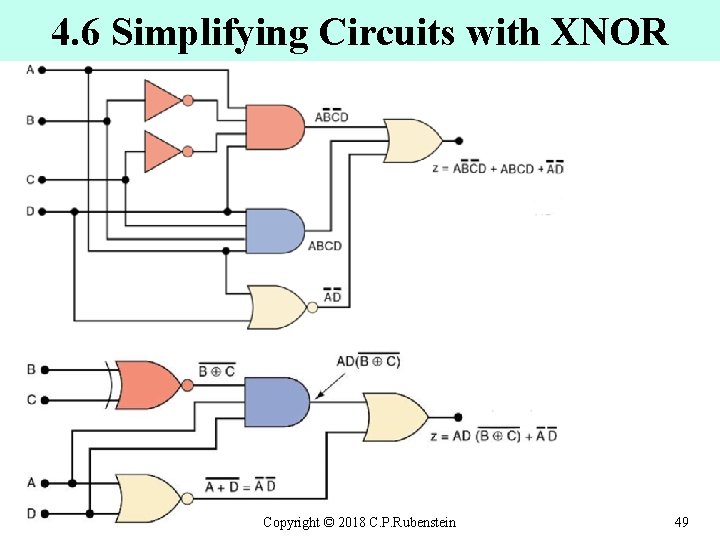
4. 6 Simplifying Circuits with XNOR Copyright © 2018 C. P. Rubenstein 49

Any Questions? Send me an email … c. rubenstein@ieee. org Copyright © 2018 C. P. Rubenstein 50

End Copyright © 2018 C. P. Rubenstein 51
- Slides: 50